An experimental proof that resistance-switching memory cells are not memristors
Abstract
It has been suggested that all resistive-switching memory cells are memristors. The latter are hypothetical, ideal devices whose resistance, as originally formulated, depends only on the net charge that traverses them. Recently, an unambiguous test has been proposed [J. Phys. D: Appl. Phys. 52, 01LT01 (2019)] to determine whether a given physical system is indeed a memristor or not. Here, we experimentally apply such a test to both in-house fabricated Cu-SiO2 and commercially available electrochemical metallization cells. Our results unambiguously show that electrochemical metallization memory cells are not memristors. Since the particular resistance-switching memories employed in our study share similar features with many other memory cells, our findings refute the claim that all resistance-switching memories are memristors. They also cast doubts on the existence of ideal memristors as actual physical devices that can be fabricated experimentally. Our results then lead us to formulate two memristor impossibility conjectures regarding the impossibility of building a model of physical resistance-switching memories based on the memristor model.
Keywords— memory materials, memristors, resistance switching memories
1 Introduction
Although some publications [1, 2] have claimed that the memristor [3] (in the ideal sense) has been found and all resistance-switching memories are memristors [4], several researchers have raised serious doubts about such claims [5, 6, 7, 8, 9, 10]. Indeed, the property of pinched hysteresis loops 222It is interesting to note that the hysteresis loops of resistance-switching memories are typically twisted, not pinched [10]. alone (“If it’s pinched it’s a memristor ” [11]) cannot serve as a good indicator of memristors since that property is shared by different types of experimentally-realizable devices (such as memristive devices and systems whose memory depends on some internal degrees of freedom, other than the charge [12]).
Remarkably, the most important characteristic of any memristor [3], namely, the functional dependence of its memory resistance (memristance), , on only the net charge, , that traverses it, , has never been demonstrated experimentally. However, it is obvious that any claim of the “memristor discovery” must be based on the experimental measurement of , and not merely on non-exclusive characteristics. Of course, since physical devices are not ideal, like any other circuit component (such as resistors, capacitors and inductors), the memristor (if found) would show some deviations from the ideal behavior, depending on the operation conditions. However, such deviations should be small, say, within 10 % of the ideal curve, for such a device to be a good representation of its ideal counterpart. Otherwise, it would be a totally different device altogether.
In Ref. [13], two of us (YVP and MD) have introduced a simple test to experimentally determine whether a resistor with memory is an ideal memristor or something else. The main idea of the test is based on the duality property of a capacitor-memristor circuit whereby, for any initial resistance state of the memristor and any form and amplitude of the applied voltage, the final state of an ideal memristor must be identical to its initial state, if the capacitor charge finally returns to its initial value [13]. In other words, our test verifies the dependence.
To prove the ideality, a scan over a large range of parameters (initial state, shape/magnitude of the applied voltage, etc.) is clearly required. To prove the opposite, however, even one or a few measurements demonstrating the absence of such a duality within the operating range of the device would be enough. Here, we report the results of more than 60 memristor tests performed over several kinds of resistance switching devices using triangular and rectangular voltage pulses of positive and negative polarities. The results of these tests are in mutual agreement, and in agreement with the theoretical modeling of Ref. [13].
In the present paper, we experimentally apply the ideal memristor test [13] to in-house fabricated Cu-SiO2 and commercially available electrochemical metallization cells as model resistance-switching devices. Electrochemical metallization cells (ECMs) [14] constitute a large family of resistance-switching devices based on the cation diffusion through a solid electrolyte. Typically, such cells exhibit bipolar resistance switching with thresholds. This property allows us to use the tested devices as representatives of the entire class of bipolar threshold-type resistance-switching cells [15], which also includes valence change memory cells (VCMs) [16]. Moreover, to demonstrate explicitly that VCMs are not memristors, we plotted the dependence of TaO devices for several driving conditions using an accurate model developed by the HP group [17]. We have found that the device resistance can not even be approximately described by the ideal relation .
Our results show that the resistance-switching memories are not memristors, and cast further doubts on the existence of ideal memristors as actual physical devices that can be fabricated in the laboratory or found in Nature. This leads us to formulate two memristor impossibility conjectures, namely that i) it is impossible to accurately model physical resistance-switching memories by adding small corrections to the ideal memristor model, and ii) it is impossible to build a circuit combining ideal memristors with any other ideal two-terminal devices (resistors, capacitors, and inductors) that emulates realistically the response of experimentally-realizable resistance-switching memories.
(a)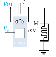 (b)
(b)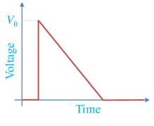
2 Methods
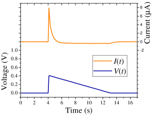
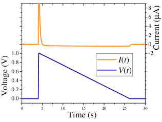
Figure 1(a) shows the experimental circuit used to implement the ideal memristor test. We used a source measure unit (Keysight B2911A) to generate the test voltage signal and control signal . The unit is controlled by a code written in C Sharp. To initialize and measure the device state, we closed the relay (part number HI05-1A 66, Standex-Meder Electronics), thus connecting the tested device to the source measure unit directly. To run the test, we opened the relay and applied the test voltage signal (such as the triangular pulse in Figure 1(b)) across the capacitor (non-polarized 1 F or 10 F capacitor) connected in series with the tested device. In this work, the test was applied to ) in-house fabricated Cu-SiO2-based electrochemical metallization memory cells, and ) commercially available ECMs by Knowm Inc. (BS-AF-W and M+SDC Cr devices) [18]. Moreover, we used a precise model of TaO VCMs (another wide class of memory devices) to show that their characteristics are in striking disagreement with the memristor model.
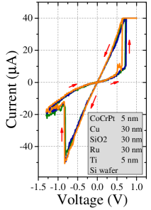
The Cu-SiO2 resistance-switching devices studied in this work were fabricated by sputtering deposition technique on the surface of a silicon wafer (substrate). A thin adhesion layer ( nm Ti) was first formed on the surface of the substrate. We used 30 nm Ru as an inert bottom electrode common for all devices. A 30-nm-thick SiO2 layer was deposited using a shadow mask with mm square openings. The top Cu electrodes of 30 nm thickness were deposited on top of SiO2 using another shadow mask with square and circular openings of various sizes (in this paper we present data for a device with a circular top electrode of m). A 5 nm CoCrPt was used as a protective layer for the top electrodes (see inset of Figure 2 for a schematic of the structure of memory cells). In order to dope SiO2 with Cu atoms [19] the devices were subjected to 580 ∘C, 1 hour annealing in He environment. After that, the samples were slowly cooled down to the room temperature. The result is a typical resistance-switching memory cell with characteristics similar to many other experimental memory devices [15]. The ideal memristor test was implemented on several randomly selected devices showing stable switching behavior.
(a) (b) (c)
Our modeling results were obtained using an accurate model of TaO VCMs [17] consisting of two equations
| (1) | |||||
| (2) | |||||
where Eq. (1) is a generalized Ohms law, while Eq. (2) describes the internal state dynamics. Here, the state variable is the volume fraction of the oxygen-depleted channel with metallic transport, while the remaining fractional volume is insulating (with nonlinear transport) [17]. According to Eq. (2), the metallic channel either expands or shrinks depending on the bias polarity. In Eq. (1), the memductance is
| (3) |
, , , , , , , are constants, and is the Heaviside step function. All simulations reported below were performed using the following set of parameter values [20]: s-1, s-1, V, V, A V, , , A-1V-1, S, S, V-1/2.
3 Results
3.1 Electrochemical metallization cells
3.1.1 Cu-SiO2 devices
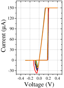
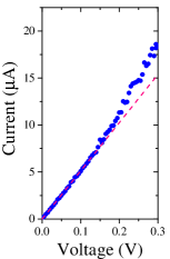
Figure 2(a) shows typical current-voltage characteristics of a selected Cu-SiO2 device. This plot demonstrates a bipolar switching with well defined thresholds, and a hysteresis loop twisted at the origin. From this plot we estimate the following parameters of our device: k, k, V, and V. Here, are the boundary resistance values and are the threshold voltages.

(a) (b) (c)
(a) (b) (c)
The ideal memristor test, as represented in Figure 1, was performed at several values of the pulse amplitude (see Figure 1(b)) with the initial memristance set to k. Here, we present the results obtained at V and V. Since these measurements were performed in sequence, the final state after the application of V served as the initial state for V. We emphasize that according to the test procedure, the initial and final charge on the capacitor is the same (zero). Therefore, if the tested device were a memristor, its final and initial memristance would be the same too.
It is found that for V the final memristance is the same as the initial one (cf. Figs. 3(a) and 3(c)). However, the larger value of V causes the device to switch into the lowest resistance state, k, see Figure 4. As the final device state is different from the initial one when the capacitor has discharged, we conclude that our device has not passed the ideal memristor test. We observed similar results for all the other samples tested. Therefore, none of our devices have passed the ideal memristor test.
We note that the test was performed using 40 A current compliance, which was not exceeded during the test. However, due to the nature of our test, its conclusions are independent of whether the current was limited or not by the compliance current. Moreover, the transition regions in the curves at s in Fig. 3 and s in Fig. 4 correspond to the capacitor discharge process. Zero current at the final moment of time indicates that the capacitor has been discharged.
3.1.2 Commercially available devices
(a)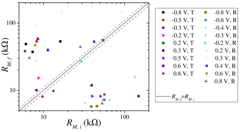 (b)
(b)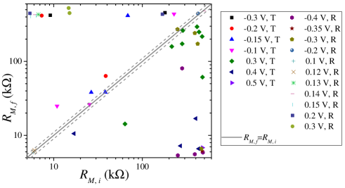
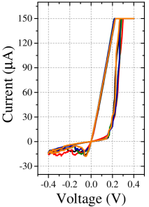
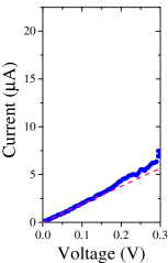
We have also applied the memristor test to commercially available EMCs [18] (Knowm, Inc,). Their operation is based on the movement of Ag atoms through a stack of chalcogenide layers with one of Ge2Se3 layers doped either by W (BS-AF-W devices) or Cr (M+SDC Cr devices). The current-voltage curves of the samples used in the memristor test are presented in Fig. 2(b) and (c). Their form indicates the bipolar resistance switching mode, similar to the one in Fig. 2(a). We note that the switching thresholds of the Knowm devices are smaller than those in our Cu-SiO2 devices. Moreover, a large k was observed in the M+SDC Cr device. To reduce the capacitor discharge time, we used a smaller F capacitor in experiments with the Knowm devices.
A series of more than 30 tests were applied to each BS-AF-W and M+SDC Cr sample. In these tests, we used the triangular (like in Fig. 1(b)) and rectangular pulses of positive and negative voltage. The width of restangular pulses was 2 s, the slope of triangular pulses was about 0.025 s. The resistance was measured using a 10 mV voltage, the waiting time before the final resistance measurement was 3 s. The pulses were applied in an arbitrary order, and the results of these measurements are summarized in Fig. 5.
Each point in Fig. 5 corresponds to a single measurement like the one in Fig. 3 or 4. For reference, the straight line represent the condition of equal initial and final states, , and dashed lines correspond to 10 % deviations from this condition. So, if the device under test were a memristor, the measurement results would group between the dashed lines. Clearly, it is not the case of both BS-AF-W and M+SDC Cr electrochemical metallization cells. In agreement with the results of Fig. 4, the tendency of for positive triangular pulses, and for negative triangular pulses can be recognized. In the case of rectangular pulses the tendency is opposite as the final state is significantly defined by the falling front of the pulse. Overall, as most of the data point are outside of the dashed line interval, the conclusion is that also the Knowm devices are not memristors.
3.2 Valence change memory cells
(a) (b)
(b)
As VCMs are the second major class of resistive memory devices, it is of interest to understand how close their behavior is to the memristor model. For this purpose, we consider the transient dynamics of TaO cells, a representative of VCMs devices, and employ Eqs. (1)-(2) to discuss their dynamics, as these have been shown to accurately reflect the experimental data [17]. Figure 6 shows the resistance as a function of charge that flows through the cell found for a set of applied voltages. One can notice that starting from the same point, the curve actually splits into individual curves for each voltage. Clearly, there is no single that ideal memristors would satisfy, or a grouping around a certain that could be taken into account by small corrections to the ideal model.
4 Discussion
4.1 Resistance-switching memories are definitely not memristors
We can further expand on these experimental results as follows. In this work we have applied the ideal memristor test suggested in Ref. [13] to in-house fabricated Cu-SiO2-based ECMs and commercially available Ag-based ECMs, which are a type of resistance-switching memories. As part of the test, we have compared the initial device states with the final ones obtained under the condition of a capacitor discharge in series with the memory device. Since in multiple tests and for a wide range of driving conditions we have found that the final states of the memory devices were quite different from the initial ones, we conclude that these resistance-switching devices cannot be described simply by a memristance that depends on the charge only: . Therefore, they are not memristors. Since the current-voltage characteristics of the devices used in our study are typical of a wide range of resistance-switching cells, our general conclusion is that resistance-switching memories are not memristors, irrespective of their specific device structures and switching mechanisms.
We also note that the triangular-shape voltage signal employed in our work has facilitated the ideal memristor test. Under the test conditions of Figure 1, the tested devices were subjected first to a relatively large positive voltage (the initial magnitude is ), followed by a small negative voltage. The tested devices failed the test since the positive voltage across the devices was sufficient to switch to , while the negative voltage was not sufficient for the inverse switching. Since, in principle, for any given pair of (positive voltage) and (negative voltage), one can always choose the test signal such that and , one can further argue that there are no ideal memristors among the threshold-type resistance-switching memory cells.
4.2 Memristor impossibility conjectures
At this juncture, the reader may ask how the ideal memristor model is related, if at all, to physical resistance-switching devices such as those studied experimentally in this work, or any other similar devices published in the literature (see, e.g., references in [15]). Accounting for the fact that the response of physical devices is different from the ideal behavior, Chua argued [4] that the resistance-switching memories are an “unfolding” theory extension of the ideal devices. More recently, he also proposed [21] that the resistance-switching can be represented by a circuit combining ideal memristors with some other ideal devices [22]. However, these statements are clearly incorrect.
In fact, unfolding relies on families of mathematical functions that are similar (close) to each other. When an idealized model is partially inadequate, the model can be improved by adding small corrections resulting in the new model: an unfolding of the original system [23, 24]. However, this approach is not applicable to the physical (experimentally-realizable) memristive devices because the difference between their physical models (as known in the literature) and the ideal memristor model can not be bridged by small correction terms. Similarly, a circuit representation of physical memory devices by circuits of ideal components is highly unlikely for the same reason: the ideal memristor behavior is too different from that of physical devices.
Based on the above arguments, we formulate two memristor impossibility conjectures that may serve as foundations for future research.
-
First memristor impossibility conjecture. It is impossible to accurately model physical resistance-switching memories by adding small corrections to the ideal memristor model.
-
Second memristor impossibility conjecture. It is impossible to accurately model physical resistance-switching memories by a circuit combining ideal memristors with any kinds of non-linear ideal circuit elements.
In the second conjecture, we refer to the ideal elements defined in Ref. [22]. It can be also formulated in the strong sense considering only the combinations of memristors with basic circuit elements (non-linear resistors, capacitors, and inductors).
5 Conclusions
In conclusion, we have employed a recently suggested test [13] to experimentally verify whether currently existing resistance-switching memories are indeed memristors, as it was claimed in Ref. [4], or not. Our results demonstrate unambiguously that they are not.
Unlike the behavior of ideal memristors, the final states of the memory devices we have measured significantly deviate from their initial states. These deviations cannot be accounted for by small corrections to the ideal memristor relations.
This study has then led us to formulate two conjectures on the impossibility of building a model of physical (experimentally-realizable) resistance-switching memories based on the ideal memristor behavior. The collection of these experimental results cast further doubts on the existence of the ideal memristor as a forth circuit element that can be fabricated experimentally. In fact, various previous results reported in the literature such as, e.g., threshold-type hysteresis curves of physical devices, stochastic switching [25, 26], and CRS behavior [27, 28] are not compatible with the memristor model and thus support our conclusions.
Acknowledgment
The authors are thankful to Mr. H. Smith and Dr. T. M. Crawford for their help with sputtering deposition. This work was partially supported by a USC Provost grant.
References
- [1] D. B. Strukov, G. S. Snider, D. R. Stewart, R. S. Williams, Nature 2008, 453, 80.
- [2] F. Z. Wang, L. Li, L. Shi, H. Wu, L. O. Chua, Journal of Applied Physics 2019, 125, 054504.
- [3] L. O. Chua, IEEE Trans. Circuit Theory 1971, 18, 507.
- [4] L. Chua, Applied Physics A 2011, 102, 765.
- [5] B. Mouttet, arXiv preprint arXiv:1201.2626 2012.
- [6] P. Meuffels, R. Soni, arXiv preprint arXiv:1207.7319 2012.
- [7] M. Di Ventra, Y. V. Pershin, Nanotechnology 2013, 24, 255201.
- [8] S. Vongehr, X. Meng, Scientific Reports 2015, 5, 11657.
- [9] K. M. Sundqvist, D. K. Ferry, L. B. Kish, Fluctuation and Noise Letters 2017, 16, 1771001.
- [10] Y. V. Pershin, M. Di Ventra, Semiconductor Science and Technology 2019, 34, 098001.
- [11] L. Chua, Semiconductor Science and Technology 2014, 29, 104001.
- [12] L. O. Chua, S. M. Kang, Proc. IEEE 1976, 64, 209.
- [13] Y. V. Pershin, M. Di Ventra, J. Phys. D: Appl. Phys. 2018, 52, 01LT01.
- [14] I. Valov, R. Waser, J. R. Jameson, M. N. Kozicki, Nanotechnology 2011, 22, 254003.
- [15] Y. V. Pershin, M. Di Ventra, Advances in Physics 2011, 60, 145.
- [16] R. Waser, R. Dittmann, G. Staikov, K. Szot, Advanced materials 2009, 21, 2632.
- [17] J. P. Strachan, A. C. Torrezan, F. Miao, M. D. Pickett, J. J. Yang, W. Yi, G. Medeiros-Ribeiro, R. S. Williams, IEEE Transactions on Electron Devices 2013, 60, 2194.
- [18] Self directed channel memristors. https://knowm.org/downloads/Knowm_Memristors.pdf. Accessed: 2020-03-20.
- [19] C. Schindler, S. C. P. Thermadam, R. Waser, M. N. Kozicki, IEEE Transactions on Electron Devices 2007, 54, 2762.
- [20] A. Ascoli, V. Ntinas, R. Tetzlaff, G. C. Sirakoulis, Electronics Letters 2017, 53, 1125.
- [21] L. O. Chua, Semiconductor Science and Technology 2019, 34, 098002.
- [22] L. O. Chua, Proc. IEEE 2003, 91, 1830.
- [23] J. Murdock, Scholarpedia 2006, 1, 1904, revision #91898.
- [24] J. W. Bruce, P. J. Giblin. Curves and Singularities: A Geometrical Introduction to Singularity Theory. Cambridge University Press, 2 edition, 1992.
- [25] S. Gaba, P. Knag, Z. Zhang, W. Lu. In 2014 IEEE International Symposium on Circuits and Systems (ISCAS). IEEE, 2014 2592–2595.
- [26] R. Naous, M. Al-Shedivat, K. N. Salama, IEEE Transactions on Nanotechnology 2016, 15, 15.
- [27] E. Linn, R. Rosezin, C. Kügeler, R. Waser, Nature materials 2010, 9, 403.
- [28] E. Linn, A. Siemon, R. Waser, S. Menzel, IEEE Transactions on Circuits and Systems I: Regular Papers 2014, 61, 2402.