Quantum Dot Arrays in Silicon and Germanium
Abstract
Electrons and holes confined in quantum dots define an excellent building block for quantum emergence, simulation, and computation. In order for quantum electronics to become practical, large numbers of quantum dots will be required, necessitating the fabrication of scaled structures such as linear and 2D arrays. Group IV semiconductors contain stable isotopes with zero nuclear spin and can thereby serve as excellent host for spins with long quantum coherence. Here we demonstrate group IV quantum dot arrays in silicon metal-oxide-semiconductor (SiMOS), strained silicon (Si/SiGe) and strained germanium (Ge/SiGe). We fabricate using a multi-layer technique to achieve tightly confined quantum dots and compare integration processes. While SiMOS can benefit from a larger temperature budget and Ge/SiGe can make ohmic contact to metals, the overlapping gate structure to define the quantum dots can be based on a nearly identical integration. We realize charge sensing in each platform, for the first time in Ge/SiGe, and demonstrate fully functional linear and two-dimensional arrays where all quantum dots can be depleted to the last charge state. In Si/SiGe, we tune a quintuple quantum dot using the N+1 method to simultaneously reach the few electron regime for each quantum dot. We compare capacitive cross talk and find it to be the smallest in SiMOS, relevant for the tuning of quantum dot arrays. These results constitute an excellent base for quantum computation with quantum dots and provide opportunities for each platform to be integrated with standard semiconductor manufacturing.
pacs:
Quantum dots have been a leading candidate for quantum computation for more than two decades Loss1998 . Furthermore, they have matured recently as an excellent playground for quantum simulation Hensgens2017 and have been proposed for the design of new states of matter Leijnse2011 ; Sau2012 . Pioneering studies in group III-V semiconductors led to proof-of-principles including the coherent control of electron spins Petta2005 ; Koppens2006 , rudimentary quantum simulations Dehollain2019 , and signatures of Majorana states Mourik2012 . The group IV semiconductors silicon and germanium have the opportunity to advance these concepts to a practical level due to their compatibility with standard semiconductor manufacturing Vandersypen2017 and the availability of isotopes with zero nuclear spin, increasing quantum coherence for single spins by four orders of magnitude Veldhorst2014 . Furthermore, heterostructures built from silicon and germanium may offer a large parameter space in which to engineer novel quantum electronic devices Zwanenburg2013b ; Sammak2019 ; Sabbagh2018 .
An initial advancement towards silicon quantum electronics Zwanenburg2013b was the design of an integration scheme based on overlapping gates to build silicon metal-oxide-semiconductor (SiMOS) quantum dots Angus2007a . This technique was later adopted in strained silicon (Si/SiGe) Zajac2015 and refined by incorporating metals with small grain size and atomic layer deposition (ALD) for layer-to-layer isolation Brauns2018 and to enable tunable coupling between single electrons in SiMOS eenink2019 . These developments in fabrication have led to a great body of results, including high-fidelity qubit operation Yang2019a ; Yoneda2018 and two-qubit logic Veldhorst2015 ; Zajac2018 ; Watson2018 . Controlling holes in silicon has been more challenging due to type II band alignment in strained silicon, limiting experiments to SiMOS Spruijtenburg2013 ; Liles2018 ; Maurand2016 . Strained germanium on the other hand Failla2016 ; Su2017 ; Sammak2019 exhibits type I band alignment and is thereby a viable platform in which holes with light effective mass Lodari2019 can be confined Hendrickx2018 and coherently controlled Hendrickx2019a . This motivates the development of an integration scheme that can build upon the individual breakthroughs realized in each platform to advance group IV semiconductor quantum dots towards large quantum systems.
Here, we present the fabrication and operation of quantum dots in silicon and germanium, in linear and two-dimensional arrays. We show stability diagrams obtained by charge sensing and report double quantum dots in SiMOS, Si/SiGe, and Ge/SiGe that can be depleted to the last charge state. We compare integration schemes and find that while each platform has unique aspects and opportunities, the core fabrication of overlapping gates defining the nano-electronic devices is remarkably similar. Fabrication is most demanding in SiMOS due to requirements on feature size, but we also find that the resulting devices have the smallest cross capacitance, simplifying tuning and operation. We leverage off the ohmic contact between quantum dots in Ge/SiGe and metals Dimoulas2006 to avoid the need for implants and to provide means for novel hybrid systems. In each case, fabrication starts from a silicon substrate, and integration is compatible with standard semiconductor technology.
Figure 1a schematically shows the SiMOS, Si/SiGe, and Ge/SiGe wafer stacks used in this study. The SiMOS 300 mm wafers are grown in an industrial complementary metal-oxide-semiconductor (CMOS) fab Petit2018 ; eenink2019 ; Sabbagh2018 , while the Si/SiGe and Ge/SiGe four-inch wafers are grown using an RP‐CVD reactor (ASM Epsilon 2000) Sammak2019 . Each platform is grown on a p-type natural Si wafer. The SiMOS structure consists of 1 m intrinsic natural silicon (iSi) followed by 100 nm 28Si (800 ppm purity) and 10 nm SiO2 Sabbagh2018 . The Si/SiGe heterostructure begins with a linearly graded Si1-xGex layer, where x ranges from 0 to 0.3. A relaxed Si0.7Ge0.3 layer of 300 nm lies below the 10 nm 28Si (800 ppm purity) quantum well which itself is separated from the 2 nm Si capping layer by a second 30 nm relaxed Si0.7Ge0.3 spacer layer. The Ge/SiGe wafer stack starts with 1.4 m of Ge and 900 nm of reverse graded Si1-xGex where x ranges from 1 to 0.8. This lies below a 160 nm Si0.2Ge0.8 spacer layer, a 16 nm Ge quantum well under compressive strain, a second Si0.2Ge0.8 layer of 22 nm and finally a thin Si cap of 1 nm Sammak2019 .
Figure 1b shows a carrier mobility versus density characterization of the three platforms. Hall bar structures were fabricated on coupons cut from the center of each wafer. Maximum mobility and critical density are extracted at 1.7 K. SiMOS 300 mm processed wafers give a peak mobility value of 1 cmVs, as well as a critical density of about 1.75 cm-2 as shown in another work Sabbagh2018 . At higher densities, SiMOS mobilities fall off due to surface roughness scattering effects Ando1982 ; Gold1986 ; Kruithof1991 . In Si/SiGe, we observe a lower critical density of 1.2 cm-2 and a significantly higher maximum mobility exceeding 1 cmVs . Similar studies conducted on natural Si/SiGe grown in an industrial CMOS fab yielded mobilities of 4.2 cmVs Wuetz2019 . This quality improvement observed by moving toward industrial CMOS fab also suggests encouraging prospects for Ge/SiGe, already exhibiting a high maximum mobility of 5 cmVs and critical density of 1.15 cm-2 despite being grown in an academic cleanroom via RP-CVD Sammak2019 .
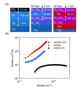
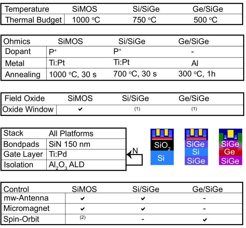
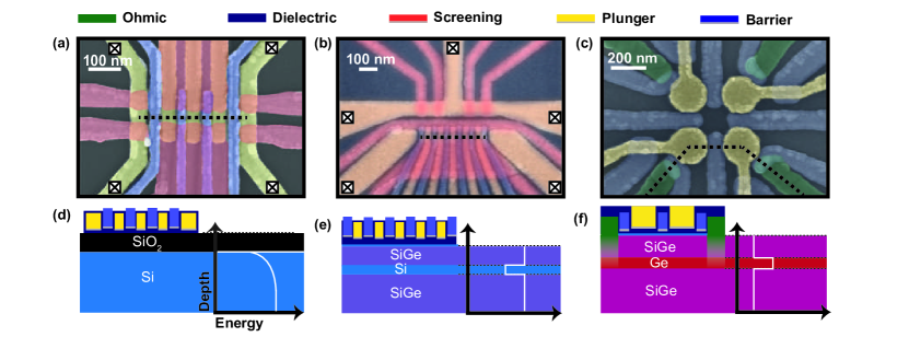
Figure 2 summarises the integration scheme utilized for each platform. The thermal budget is estimated based on the respective limiting mechanisms. For SiMOS, thermal processing is limited by the self-diffusion of natural silicon from the substrate into the 28Si epilayer. From the self diffusion constants measured by Bracht et al. Bracht1998 , we estimate the point at which the residual 29Si concentration within 1 nm of the Si-SiO2 interface increases by 1 ppm occurs at 1000 oC for time scales above 1 hour, for furnace anneals in a pure argon atmosphere. Consequently, this allows for extensive thermal treatment and annealing of samples. This is highly advantageous, as we have observed that a 15 minute anneal in forming gas at 400 oC after the deposition of every gate layer greatly improves the quality of our fine features (see Supporting Information section Ia for detailed comparison). In addition, a final end-of-line anneal is conducted to eliminate processing damage at 400 oC in forming gas for 30 minutes. In the cases of Si/SiGe and Ge/SiGe, the thermal budget is limited by strain relaxation of the quantum wells, thus the maximum processing thermal budget is given qualitatively by the temperature at which the quantum wells were grown. This is 750 oC for strained Si and 500 oC for strained Ge Sammak2019 .
The design of ohmic contacts is tailored to the specific requirements of the device. For both Si platforms, ohmic contact is made via high fluence P ion implantation followed by evaporation of Ti:Pt metallic contacts, creating n++ doped, low resistance channels. The oxide is etched locally directly before metal deposition using buffered hydrofluoric acid (BHF). In the case of Si/SiGe, stray capacitance is minimized to ensure maximum power is dissipated in the variable resistance of the sensing quantum dot for RF-readout. Germanium can make direct ohmic contact to metals Dimoulas2006 , avoiding the need for implants. We deposit Al and anneal at 300 oC for 1 hour in vacuum to assist in Al diffusion into the quantum well. The Al ohmic is defined close to the quantum dots, resulting in a very low resistance channel ideally suited for RF circuits and enabling a tunnel contact that can even be made superconducting Hendrickx2019 . The implementation does however lower the thermal budget of further processing.
Fabrication of each device utilizes a titanium-palladium (Ti:Pd) gate stack with 3 nm of Ti deposited for each layer to assist with adhesion. Pd makes a good gate metal due to its low grain size Brauns2018 . Unlike the commonly used material Al, Pd does not self-oxidise and ALD can be used to define sharp dielectric interfaces. For the SiMOS and Si/SiGe devices shown in Fig. 3, we utilize a three layer gate stack that we refer to as the screening layer, the plunger layer and the barrier layer. In order to assist climbing of overlapping gate features, the initial layer is deposited at 20 nm total thickness, while subsequent layers at 40 nm. Each layer is isolated from one another via ALD of Al2O3 at 7 nm thickness. We measure the dielectric strength of our Al2O3 to be greater than 6 MV/cm, allowing potentials of greater than 4 V to be applied between adjacent gates. To leverage off the high quality industrial CMOS fab, we begin fabrication of SiMOS devices on wafers including a 10 nm SiO2 oxide already grown. To further reduce likelihood of leakage from gate to substrate, we first grow a thick 10 nm Al2O3 blanket layer over the entirety of the substrate. Advantageously, one can etch Al2O3 on thermally grown SiO2 selectively, allowing the definition of a 20x20 m2 area where the quantum dot system is defined, which we have measured to significantly reduce low-frequency drifts deduced from charge occupation stability Connors2019 (see Supporting Information section Ib for comparison).
The final deposition step is the qubit control layer. The spin-orbit coupling for holes in germanium enables qubit operation by simply applying microwave pulses to the quantum dot gates Watzinger2018 ; Hendrickx2019a and no further processing is required. In silicon, qubit driving can be realized by integrating on-chip striplines Veldhorst2014 , which we fabricate using Al or NbTiN, or micromagnets Kawakami2014 , which we integrate using Ti:Co. Quantum dots in Si/SiGe generally have a larger and more mobile electron wave function as compared to SiMOS and thereby benefit most from a micromagnet integration for fast qubit driving.
A schematic of each material and associated device is shown in Fig. 3 and labelling of the relevant gates are shown in Fig. 4. The SiMOS device is a three-layer, triple quantum dot structure with dedicated plungers (P1-3), inter-dot barriers (B12, B23) and reservoir barriers (Tl, Tr). Charge noise resulting from fluctuations of impurities near the quantum dot array is screened by two large metallic gates (C, C) deposited in the initial layer and kept at constant potential. These also serve to confine the quantum dots in one lateral dimension. Two single electron transistors (SETs) are positioned at either side of the quantum dot array, and function as charge sensors for spin and charge readout. The Si/SiGe device is a quintuple quantum dot linear array written in three layers utilizing a similar architecture to that of the SiMOS device. The dot array contains five plunger gates (P1-5) with inter-dot barriers (B12-45) and reservoir barriers. Dots are confined laterally and screened from charge noise by two confinement gates. Two SETs are positioned parallel to the dot channel. The Ge/SiGe device is a 2x2 quadruple quantum dot array written in two layers. Gates (P1-4) are positioned anti-clockwise in the array and define the potential of the dots. Each pair of adjacent dots share a barrier gate (B12-41) capable of tuning inter-dot tunnel coupling. Coupling of each dot to its reservoir can be controlled via a barrier gate. This device can be operated as a quadruple quantum dot system in transport mode, but for the present work we intentionally tune the inter-dot barrier to form a single hole transistor (SHT) along a dot channel that we subsequently use for charge sensing of the double quantum dot along the opposite channel. For more information about device specific fabrication, see Supporting Information section II.
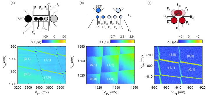
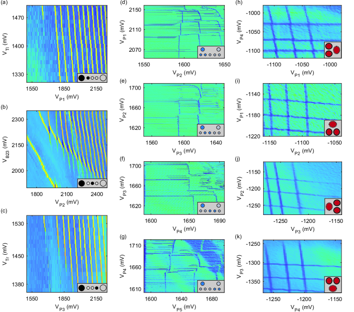
To demonstrate the success of our integration scheme, we show that we can create stable quantum dots in each platform. Figure 4 shows charge stability diagrams for tunnel-coupled double quantum dots, measured by performing charge sensing. Lock-in techniques are used in the case of SiMOS and Ge/SiGe, where an excitation is placed on an inter-dot barrier gate B12 in each case, and the trans-conductance of our source-drain channel is measured. We use compensation to remain at a sensitive point on our SET/SHT Coulomb peaks Yang2011 . In the case of Si/SiGe, charge readout is performed using RF-reflectometry techniques. A 3 H kinetic inductor is bonded to the sample source which forms a resonant LC circuit when combined with parasitic capacitance to ground. In each case we measure a stability diagram and show that we can deplete down to the (0,0) electron/hole charge configuration. We note that the plunger voltages in the case of Si/SiGe required to form double quantum dots in the (1,1) charge occupation are within a charging energy. These remarkably similar tuning parameters are promising with regards to the stringent requirements placed on quantum dot array tune-up in crossbar architectures Li2018 . While operation in the single electron regime in silicon has been routinely achieved before, this work shows the first demonstration of the single hole regime using charge sensing of holes in Ge/SiGe. We attribute the slight difference in slope of the first and second charge addition lines in Fig. 4c to a shift in the position of the dot relative to the inter-dot tunnel barrier.
In Fig 5. we demonstrate that quantum dots can be formed under each dedicated plunger gate. For Fig. 5 (a-c), in each SiMOS quantum dot, lock-in charge sensing is performed by placing an excitation on the respective plunger gates, while trans-conductance in the nearby SET channel is measured. In each case, the first charge transition is visible. For quantum dots formed under plungers P2-3, electron loading is from the right SET which constitutes a reservoir. For the dot under P1, loading is from the left SET via the gate Tl. The Si/SiGe quintuple quantum dot system in Fig 5(d-g) is tuned using the N+1 strategy Volk2019 , reaching the few-electron regime simultaneously for all quantum dots. In Fig. 5 we show stability diagrams, in each of which we scan two virtual plunger gates which allow to controllably load a single electron into each quantum dot. Double quantum dots are formed between each set of adjacent plungers, and sensed using RF-reflectometry like in Fig. 4b using the left SET for all configurations. As expected, observable signal from charge transition lines fades as the dot pairs are formed farther away from the SET. The derivative of the reflected signal is plotted, and shows the (0,0) charge occupancy for each charge stability diagram. For every double dot, loading occurs via the left accumulation gate, leading to latching effects and low tunnel rates in the dots formed farther away from the reservoir. Here, the plunger voltages, while similar, are not entirely within a charging energy, suggesting further improvements to heterostructure uniformity are required to meet strict large scale array tune-up requirements. Figure 5 (h-k) shows charge sensing operation of the 2x2 quantum dot array fabricated in Ge/SiGe. In each case, a sensing dot is formed in the channel parallel to the double dot by opening the inter-dot barrier such that a large single dot is formed. In the opposite channel, the inter-dot barrier is closed, forming a double dot system in the low tunnel coupled regime.
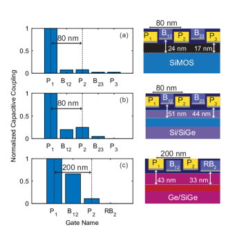
A significant challenge for larger quantum dot arrays will manifest in tuning. The presence of large capacitive crosstalk in GaAs has led to development of virtual gates and approaches to tune larger systems Baart2016 ; Volk2019 . To assess the relevance of these approaches for silicon and germanium structures we measure cross capacitance as show in Fig. 6. To obtain the cross coupling, we measure the slope of the charge addition lines with respect to each gate and normalize by a cross coupling of unity for the plunger gate associated with the respective quantum dot. Each slope is taken for the first charge transition and in the low tunnel-coupled regime. In SiMOS, cross coupling is almost negligible, as expected from quantum dots located only 17 nm (10 nm SiO2 and 7 nm Al2O3) below the electric gates. This compares favourably to the cross coupling observed in Si/SiGe, where falloff is significantly slower despite sharing equal gate pitch to the SiMOS array. While the cross coupling in the Ge/SiGe system is the largest and extends over multiple neighbouring gates, it still falls off significantly faster than quantum dots defined in GaAs Volk2019 . For Ge/SiGe, we also observe that the barrier gates have a relatively stronger coupling as compared to the plunger gates, due to definition in lower layers of the multi-layer stack. Summarizing, we conclude that for SiMOS tuning is most straightforward considering capacitive cross talk only, while each platform compares favourably to GaAs.
In conclusion we presented a cross-platform integration scheme for multi-layer quantum dot arrays in group-IV semiconductor hosts. We successfully fabricated linear and 2D arrays of quantum dots and in the group IV platforms SiMOS, Si/SiGe and Ge/SiGe. We demonstrated single electron and hole occupancy in double quantum dots confirmed by charge sensing. We showed stable quantum dots under each plunger in a SiMOS triple dot linear array, depleteable to the final charge state. In Si/SiGe, we demonstrated tune-up of a quintuple dot array utilizing the N+1 method, successfully reaching the few electron regime in each dot simultaneously. Moreover, we showed we could form and sense double dots in the single hole regime in each configuration of a 2x2 quadruple quantum dot array in Ge/SiGe. We furthermore compared the capacitive cross talk between quantum dots and gates. We find that the cross capacitance can be small and therefore argue that future work on strategies for the initial tuning of quantum dot arrays should address disorder rather than capacitive cross talk, in particular for SiMOS quantum dots. We envision that our realization of an integration scheme to build quantum dots in SiMOS, Si/SiGe, and Ge/SiGe will boost the collective development toward large quantum dot arrays to build, simulate, and compute with quantum information.
.
Acknowledgements
M.V. acknowledges funding by the Netherlands Organization of Scientific Research (NWO) for a VIDI grant and for a projectruimte. The authors are grateful for support from Intel. Research was sponsored by the Army Research Office (ARO) and was accomplished under Grant No. W911NF- 17-1-0274. The views and conclusions contained in this document are those of the authors and should not be interpreted as representing the official policies, either expressed or implied, of the Army Research Office (ARO), or the U.S. Government. The U.S. Government is authorized to reproduce and distribute reprints for Government purposes notwithstanding any copyright notation herein.
References
- (1) Loss, D.; DiVincenzo, D. P. Physical Review A - Atomic, Molecular, and Optical Physics 1998, 57, 120–126.
- (2) Hensgens, T.; Fujita, T.; Janssen, L.; Li, X.; Van Diepen, C. J.; Reichl, C.; Wegscheider, W.; Das Sarma, S.; Vandersypen, L. M. Nature 2017, 548, 70–73.
- (3) Leijnse, M.; Flensberg, K. Physical Review B - Condensed Matter and Materials Physics 2011, 84, 140501.
- (4) Sau, J. D.; Sarma, S. D. Nature Communications 2012, 3, 964.
- (5) Petta, J. R.; Johnson, A. C.; Taylor, J. M.; Laird, E. A.; Yacoby, A.; Lukin, M. D.; Marcus, C. M.; Hanson, M. P.; Gossard, A. C. Science 2005, 309, 2180–2184.
- (6) Koppens, F. H.; Buizert, C.; Tielrooij, K. J.; Vink, I. T.; Nowack, K. C.; Meunier, T.; Kouwenhoven, L. P.; Vandersypen, L. M. Nature 2006, 442, 766–771.
- (7) Dehollain, J. P.; Mukhopadhyay, U.; Michal, V. P.; Wang, Y.; Wunsch, B.; Reichl, C.; Wegscheider, W.; Rudner, M. S.; Demler, E.; Vandersypen, L. M. K. arXiv e-prints 2019, arXiv:1904.05680.
- (8) Mourik, V.; Zuo, K.; Frolov, S. M.; Plissard, S. R.; Bakkers, E. P.; Kouwenhoven, L. P. Science 2012, 336, 1003–1007.
- (9) Vandersypen, L. M. K.; Bluhm, H.; Clarke, J. S.; Dzurak, A. S.; Ishihara, R.; Morello, A.; Reilly, D. J.; Schreiber, L. R.; Veldhorst, M. npj Quantum Information 2016, 3, 34.
- (10) Veldhorst, M.; Hwang, J. C.; Yang, C. H.; Leenstra, A. W.; De Ronde, B.; Dehollain, J. P.; Muhonen, J. T.; Hudson, F. E.; Itoh, K. M.; Morello, A.; Dzurak, A. S. Nature Nanotechnology 2014, 9, 981–985.
- (11) Zwanenburg, F. A.; Dzurak, A. S.; Morello, A.; Simmons, M. Y.; Hollenberg, L. C.; Klimeck, G.; Rogge, S.; Coppersmith, S. N.; Eriksson, M. A. Reviews of Modern Physics 2013, 85, 961–1019.
- (12) Sammak, A.; Sabbagh, D.; Hendrickx, N. W.; Lodari, M.; Paquelet Wuetz, B.; Tosato, A.; Yeoh, L. R.; Bollani, M.; Virgilio, M.; Schubert, M. A.; Zaumseil, P.; Capellini, G.; Veldhorst, M.; Scappucci, G. Advanced Functional Materials 2019, 29, 1807613.
- (13) Sabbagh, D. et al. Phys. Rev. Applied 2019, 12, 014013.
- (14) Angus, S. J.; Ferguson, A. J.; Dzurak, A. S.; Clark, R. G. Nano Letters 2007, 7, 2051–2055.
- (15) Zajac, D. M.; Hazard, T. M.; Mi, X.; Wang, K.; Petta, J. R. Applied Physics Letters 2015, 106, 223507.
- (16) Brauns, M.; Amitonov, S. V.; Spruijtenburg, P. C.; Zwanenburg, F. A. Scientific Reports 2018, 8, 5690.
- (17) Eenink, H. G. J.; Petit, L.; Lawrie, W. I. L.; Clarke, J. S.; Vandersypen, L. M. K.; Veldhorst, M. arXiv e-prints 2019, arXiv:1907.08523.
- (18) Yang, C. H.; Chan, K. W.; Harper, R.; Huang, W.; Evans, T.; Hwang, J. C.; Hensen, B.; Laucht, A.; Tanttu, T.; Hudson, F. E.; Flammia, S. T.; Itoh, K. M.; Morello, A.; Bartlett, S. D.; Dzurak, A. S. Nature Electronics 2019, 2, 151–158.
- (19) Yoneda, J.; Takeda, K.; Otsuka, T.; Nakajima, T.; Delbecq, M. R.; Allison, G.; Honda, T.; Kodera, T.; Oda, S.; Hoshi, Y.; Usami, N.; Itoh, K. M.; Tarucha, S. Nature Nanotechnology 2018, 13, 102–106.
- (20) Veldhorst, M.; Yang, C. H.; Hwang, J. C.; Huang, W.; Dehollain, J. P.; Muhonen, J. T.; Simmons, S.; Laucht, A.; Hudson, F. E.; Itoh, K. M.; Morello, A.; Dzurak, A. S. Nature 2015, 526, 410–414.
- (21) Zajac, D. M.; Sigillito, A. J.; Russ, M.; Borjans, F.; Taylor, J. M.; Burkard, G.; Petta, J. R. Science 2018, 359, 439–442.
- (22) Watson, T. F.; Philips, S. G.; Kawakami, E.; Ward, D. R.; Scarlino, P.; Veldhorst, M.; Savage, D. E.; Lagally, M. G.; Friesen, M.; Coppersmith, S. N.; Eriksson, M. A.; Vandersypen, L. M. Nature 2018, 555, 633–637.
- (23) Spruijtenburg, P. C.; Ridderbos, J.; Mueller, F.; Leenstra, A. W.; Brauns, M.; Aarnink, A. A.; Van Der Wiel, W. G.; Zwanenburg, F. A. Applied Physics Letters 2013, 102, 192105.
- (24) Liles, S. D.; Li, R.; Yang, C. H.; Hudson, F. E.; Veldhorst, M.; Dzurak, A. S.; Hamilton, A. R. Nature Communications 2018, 9, 3255.
- (25) Maurand, R.; Jehl, X.; Kotekar-Patil, D.; Corna, A.; Bohuslavskyi, H.; Laviéville, R.; Hutin, L.; Barraud, S.; Vinet, M.; Sanquer, M.; De Franceschi, S. Nature Communications 2016, 7, 13575.
- (26) Failla, M.; Keller, J.; Scalari, G.; Maissen, C.; Faist, J.; Reichl, C.; Wegscheider, W.; Newell, O. J.; Leadley, D. R.; Myronov, M.; Lloyd-Hughes, J. New Journal of Physics 2016, 18, 113036.
- (27) Su, Y. H.; Chuang, Y.; Liu, C. Y.; Li, J. Y.; Lu, T. M. Physical Review Materials 2017, 1, 044601.
- (28) Lodari, M.; Tosato, A.; Sabbagh, D.; Schubert, M. A.; Capellini, G.; Sammak, A.; Veldhorst, M.; Scappucci, G. Physical Review B 2019, 100, 041304.
- (29) Hendrickx, N. W.; Franke, D. P.; Sammak, A.; Kouwenhoven, M.; Sabbagh, D.; Yeoh, L.; Li, R.; Tagliaferri, M. L.; Virgilio, M.; Capellini, G.; Scappucci, G.; Veldhorst, M. Nature Communications 2018, 9, 2835.
- (30) Hendrickx, N. W.; Franke, D. P.; Sammak, A.; Scappucci, G.; Veldhorst, M. arXiv e-prints 2019, arXiv:1904.11443.
- (31) Dimoulas, A.; Tsipas, P.; Sotiropoulos, A.; Evangelou, E. K. Applied Physics Letters 2006, 89, 252110.
- (32) Petit, L.; Boter, J. M.; Eenink, H. G.; Droulers, G.; Tagliaferri, M. L.; Li, R.; Franke, D. P.; Singh, K. J.; Clarke, J. S.; Schouten, R. N.; Dobrovitski, V. V.; Vandersypen, L. M.; Veldhorst, M. Physical Review Letters 2018, 121, 076801.
- (33) Ando, T.; Fowler, A. B.; Stern, F. Reviews of Modern Physics 1982, 54, 437–672.
- (34) Gold, A.; Dolgopolov, V. T. Physical Review B 1986, 33, 1076–1084.
- (35) Kruithof, G. H.; Klapwijk, T. M.; Bakker, S. Physical Review B 1991, 43, 6642–6649.
- (36) Paquelet Wuetz, B.; Bavdaz, P. L.; Yeoh, L. A.; Schouten, R.; van der Does, H.; Tiggelman, M.; Sabbagh, D.; Sammak, A.; Almudever, C. G.; Sebastiano, F.; Clarke, J. S.; Veldhorst, M.; Scappucci, G. arXiv e-prints 2019, arXiv:1907.11816.
- (37) Jock, R. M.; Jacobson, N. T.; Harvey-Collard, P.; Mounce, A. M.; Srinivasa, V.; Ward, D. R.; Anderson, J.; Manginell, R.; Wendt, J. R.; Rudolph, M.; Pluym, T.; Gamble, J. K.; Baczewski, A. D.; Witzel, W. M.; Carroll, M. S. Nature Communications 2018, 9, 1768.
- (38) Huang, W.; Veldhorst, M.; Zimmerman, N. M.; Dzurak, A. S.; Culcer, D. Physical Review B 2017, 95, 075403.
- (39) Bracht, H.; Haller, E. E.; Clark-Phelps, R. Physical Review Letters 1998, 81, 393–396.
- (40) Hendrickx, N. W.; Tagliaferri, M. L.; Kouwenhoven, M.; Li, R.; Franke, D. P.; Sammak, A.; Brinkman, A.; Scappucci, G.; Veldhorst, M. Physical Review B 2019, 99, 075435.
- (41) Connors, E. J.; Nelson, J.; Qiao, H.; Edge, L. F.; Nichol, J. M. arXiv e-prints 2019, arXiv:1907.07549.
- (42) Volk, C.; Zwerver, A. M. J.; Mukhopadhyay, U.; Eendebak, P. T.; van Diepen, C. J.; Dehollain, J. P.; Hensgens, T.; Fujita, T.; Reichl, C.; Wegscheider, W.; Vandersypen, L. M. K. npj Quantum Information 2019, 5, 29.
- (43) Watzinger, H.; Kukučka, J.; Vukušić, L.; Gao, F.; Wang, T.; Schäffler, F.; Zhang, J. J.; Katsaros, G. Nature Communications 2018, 9, 3902.
- (44) Kawakami, E.; Scarlino, P.; Ward, D. R.; Braakman, F. R.; Savage, D. E.; Lagally, M. G.; Friesen, M.; Coppersmith, S. N.; Eriksson, M. A.; Vandersypen, L. M. Nature Nanotechnology 2014, 9, 666–670.
- (45) Yang, C. H.; Lim, W. H.; Zwanenburg, F. A.; Dzurak, A. S. AIP Advances 2011, 1, 042111.
- (46) Li, R.; Petit, L.; Franke, D. P.; Dehollain, J. P.; Helsen, J.; Steudtner, M.; Thomas, N. K.; Yoscovits, Z. R.; Singh, K. J.; Wehner, S.; Vandersypen, L. M.; Clarke, J. S.; Veldhorst, M. Science Advances 2018, 4, eaar3960.
- (47) Baart, T. A.; Shafiei, M.; Fujita, T.; Reichl, C.; Wegscheider, W.; Vandersypen, L. M. Nature Nanotechnology 2016, 11, 330–334.
Supporting Information
I SiMOS Fabrication Improvements
I.1 Gate Anneal
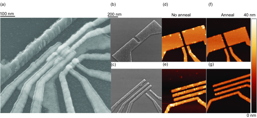
In silicon MOS, anneals are generally used to repair damage caused by e-beam exposure and to improve the structural quality of metal gates. We find that for SiMOS quantum dot devices, the quality of the gates can be improved by the incorporation of a forming gas anneal at 400 ∘C for 15 min after each gate deposition. Supporting Figure 1(a) shows a scanning electron microscope (SEM) image of a device for which the anneal was implemented. Supporting Figures 1(b)-(g) show SEM and Atomic Force Microscopy (AFM) images for two gate layers of a SiMOS device. We observe a large reduction of surface roughness and sidewall height, which improves even further the homogeneity and yield of the metallic gates.
I.2 ALD Window Etch
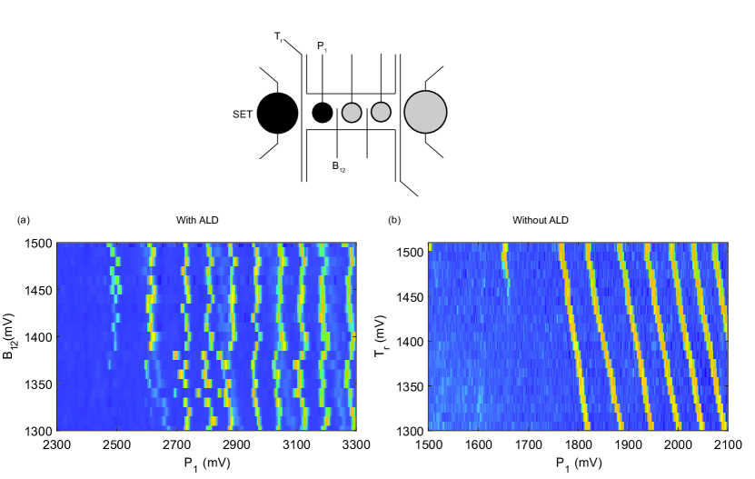
Incorporating atomic layer deposition (ALD) of Al2O3 into the gate stack introduces further sources of charge noise Connors2019 making it undesirable in the active region of spin qubits. On the other hand, it is necessary to prevent inter-gate leakage when utilizing a Ti:Pd multi-layer gate stack, as well as leakage to substrate. In the case of SiMOS, fabrication begins on a 10 nm SiO2 dielectric grown across the substrate. While high in quality, due to the sheer area overlap of gate fan-out, there is a non-negligible probability that a gate may overlap with a region of damaged dielectric. To prevent leakage of gate layers to substrate in our SiMOS stack, we find an initial blanket layer of Al2O3 is necessary. An etching process (see Supp. Info. section II regarding fabrication details) with a high selectivity of Al2O3 over SiO2 allows us to locally remove this layer in the active region. Supporting Figure 2 shows charge stability diagrams of two identically processed quantum dot devices in SiMOS where Al2O3 was present or where an oxide window was etched. Without etching, charge noise causes significant fluctuations in the quantum dot potential, which can be observed from the constantly shifting charge addition lines in Supporting Fig. 2a. Instead, when an oxide window is etched, we observe stable transitions, see Supporting Fig. 2b. We attribute this stability to the removal of the ALD layer beneath the first gate layer. We note that this behaviour is reproducible in and consistent with other SiMOS quantum dot devices fabricated with and without the removal of the initial ALD layer in the quantum dot active region.
II Extended Fabrication Recipe
Here we present the full fabrication process for each platform, specifically for the devices fabricated and studied in the main text.
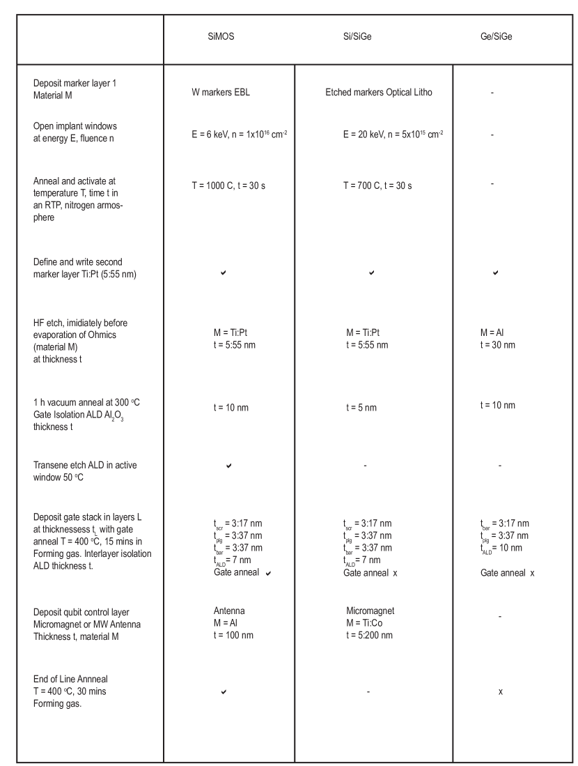
In the case of SiMOS, fabrication begins on a natural silicon wafer, with 1 um of intrinsic silicon grown, followed by 100 nm epilayer 28Si, and a 10 nm thermally grown oxide Sabbagh2018 . First, tungsten (W) markers are patterned, which are used to define implant windows via electron beam lithography (EBL). After exposure, phosphorus ions (P+) at 6 keV are implanted to create highly negatively doped (n++) regions in each die. An activation anneal is conducted in a rapid thermal processor (RTP) at 1000 oC for 30 seconds. A buffered hydro-fluoric (BHF) etch removes oxide in bond-pad areas, where Ti:Pt (5:55 nm) metallic contacts are deposited, creating ohmic contacts. A second layer of Ti:Pt markers are also written in this step. Next, a blanket Al2O3 ALD layer of 10 nm is grown across the entire sample. A small 20 x 20 m2 area is exposed and etched away in the vicinity of the quantum dot formation area. This improves dot stability (see above). Large rounded rectangular regions are then exposed in regions where wirebonding is expected, and 150 nm of SiN is sputtered. These create safer bondpads with which to bond to, reducing leakage and improving device yield. The SiMOS device presented in the work utilizes a three layer Ti:Pd gate stack. (3:17, 3:37, 3:37 nm). After each layer, the device is annealed in a RTP furnace for 15 minutes at 400 oC in forming gas, then a layer of ALD is grown at 7 nm thickness. Next, the qubit control layer is deposited. This can either be an Al or NbTiN antenna of 100 nm thickness for Electron spin resonance driving, or a Ti:Co micromagnet (5:195 nm) for Electron dipole spin resonance. The final step is an end of line anneal at 400 oC for 30 minutes in forming gas in a RTP.
The Si/SiGe 5 dot linear array begins on a natural silicon substrate. A linearly graded Si1-xGex layer is deposited where x ranges from 0 to 0.3. A relaxed Si0.7Ge0.3 layer of 300 nm lies below the 10 nm 28Si (800 ppm purity) quantum well which itself is separated from the 2 nm Si capping layer by a second 30 nm relaxed Si0.7Ge0.3 spacer layer. The initial marker layer is written using optical lithography and is formed by etching away the SiO2. Next, a BHF dip removes native oxide selectively where ohmic contacts of Ti:Pt (5:55 nm) are evaporated, alongside a second set of markers.
Gate stack fabrication of the device is almost identical to that of SiMOS. It is a 3-layer Ti:Pd stack of the same thicknesses, interlayer isolated via 7 nm of Al2O3. However, we do not employ a gate anneal between gate layers, despite this technically being possible within the context of thermal budget. For control, both striplines and micromagnets are avaliable, however we prefer the electrical driving option since electron wavefunctions in Si/SiGe tend to be more mobile and hence EDSR provides a route to faster driving. We do not conduct an end of line anneal on SiGe devices.
For the fabrication of the Ge/SiGe 2x2 array, we begin with a natural silicon substrate, upon which 1.4 m of Ge and 900 nm of reverse graded Si1-xGex where x ranges from 1 to 0.8 is grown. This lies below a 160 nm Si0.2Ge0.8 spacer layer, a 16 nm Ge quantum well under compressive strain, a second Si0.2Ge0.8 layer of 22 nm and finally a thin Si cap of 1 nmSammak2019 . Ti:Pt EBL markers are then defined for future alignment. A short HF acid etch is conducted immidiately before depositing 30 nm Al on regions where ohmic contact is desired. An advantage of the Ge/SiGe platform is the possibility of ohmic formation extremely close (within nm) of the quantum dot. Devices are then placed under vacuum for 1 h at 300 oC causing Al to diffuse through the heterostructure into the quantum well forming ohmic contact. Atomic Layer Deposition is then performed covering the sample in a 10 nm Al2O3 blanket. The gate stack consists of two layers, barrier and plunger. The barrier layer is deposited at 20 nm total thickness utilizing the Ti:Pd stack (3:17 nm). The plunger layer is deposited at 40 nm total thickness (3:37 nm). No further processing is required as the large intrinsic Spin-Orbit coupling of holes in Ge/SiGe provides a native electric driving mechanismHendrickx2019a .
References
- (1) Connors, E. J.; Nelson, J.; Qiao, H.; Edge, L. F.; Nichol, J. M. arXiv e-prints 2019, arXiv:1907.07549.
- (2) Sabbagh, D. et al. Phys. Rev. Applied 2019, 12, 014013.
- (3) Sammak, A.; Sabbagh, D.; Hendrickx, N. W.; Lodari, M.; Paquelet Wuetz, B.; Tosato, A.; Yeoh, L. R.; Bollani, M.; Virgilio, M.; Schubert, M. A.; Zaumseil, P.; Capellini, G.; Veldhorst, M.; Scappucci, G. Advanced Functional Materials 2019, 29, 1807613.
- (4) Hendrickx, N. W.; Franke, D. P.; Sammak, A.; Scappucci, G.; Veldhorst, M. arXiv e-prints 2019, arXiv:1904.11443.