Hanbury Brown and Twiss Exchange Correlations in Graphene Box
Abstract
Quadratic detection in linear mesoscopic transport systems produces cross terms that can be viewed as interference signals reflecting statistical properties of charge carriers. In electronic systems these cross term interferences arise from exchange effects due to Pauli principle. Here we demonstrate fermionic Hanbury Brown and Twiss (HBT) exchange phenomena due to indistinguishability of charge carriers in a diffusive graphene system. These exchange effects are verified using current-current cross correlations in combination with regular shot noise (autocorrelation) experiments at microwave frequencies. Our results can be modeled using semiclassical analysis for a square-shaped metallic diffusive conductor, including contributions from contact transparency. The experimentally determined HBT exchange factor values lie between the calculated ones for coherent and hot electron transport.
I Introduction
Shot noise is a widely used characterization method in nanophysics, as it can provide more information of the charge transport than conventional conductance or thermal noise measurements Kogan (1996); Blanter and Büttiker (2000); Martin (2005); Lesovik and Sadovskyy (2011). Multiterminal current-current correlation experiments provide additional insight to intrinsic characteristics of charge carriers in mesoscopic systems. For example, they allow one to distinguish bosonic and fermionic carriers Liu et al. (1998); Oliver (1999); Henny et al. (1999).
Many of the noise and cross correlation experiments probing fundamental properties of the charge carriers have been performed using edge states in the quantum Hall regime, in which quantum point contacts with tunable transparency control the propagation of coherent beams of electrons or composite fermions Glattli (2005). In this setup, one can perform two-particle scattering experiments and observe Hanbury Brown and Twiss R. Hanbury Brown and Twiss (1956) (HBT) interference effects in current-current cross correlation Neder et al. (2007), which are not visible in Aharonov-Bohm conductance experiments. In a regular mesoscopic conductor the phase-dependent phenomena in two-particle scattering events are averaged out over many possible trajectoriesBlanter and Büttiker (1997). However, even after such averaging current-current cross correlations in different terminals are affected by Fermi statistics of electrons in a non-trivial way. One well known consequence of Fermi statistics is the negative sign of cross correlations between the currents in different terminals Blanter and Büttiker (2000). In this work we investigate another interesting consequence – non-additive nature of cross correlations Blanter and Büttiker (1997); Sukhorukov and Loss (1999) – in a HBT setup R. Hanbury Brown and Twiss (1956); Neder et al. (2007) with two sources and two detectors attached to a diffusive graphene flake. Below we will refer to the non-additivity of the noise cross correlations as HBT exchange effect.
To our knowledge, only one experiment has so far addressed HBT exchange effects in diffusive conductors. Cross correlations and HBT exchange were measured in a cross-shaped graphene conductor in which the charge carrier density, and thereby the screening of impurities, could be tuned by the back gate voltage Tan et al. (2018). According to the theory, in a diffusive conductor with cross geometry the paths of scattering electrons are quite restricted, and the HBT exchange effect should disappear Blanter and Büttiker (1997); Sukhorukov and Loss (1999). However, the experiment showed a finite exchange effect, which was attributed to an appreciable mean free path of electrons, comparable to the size of the crossing.
In charge neutral graphene, ideally, electrical transport takes place via evanescent waves, the distribution of which mimics diffusive electron transport Katsnelson (2006); Tworzydło et al. (2006); San-Jose et al. (2007); Lewenkopf et al. (2008). Since the evanescent waves may propagate to both measuring terminals, special cross correlations are obtained in graphene near the charge neutrality point (CNP) Laakso and Heikkilä (2008). According to the tight binding calculations of Ref. Laakso and Heikkilä (2008), there is negative HBT exchange effect at the Dirac point. Instead of diffusive-like shot noise due to evanescent waves, experiments have shown more complex behavior in graphene DiCarlo et al. (2008); Danneau et al. (2008a, 2009). For graphene ribbons, Coulomb blockade effects and localization have been found to influence the shot noise results substantially Danneau et al. (2010). Therefore, also shot noise cross-correlations can be expected to differ from those appearing in pure diffusive transport and to exhibit features inherent to disordered graphene samples.
In this work we study HBT exchange effect in coherent square-shaped graphene conductor with short mean free path and diffusive transport of electrons. We measure both current-current cross correlations at microwave frequencies and regular shot noise of the contacts (autocorrelation). We model our results using semiclassical analysis for a diffusive coherent conductor, in which the noise arises locally due to the non-equilibrium distribution of electrons. We repeat the analysis in the hot electron regime, where the noise is characterized by local temperature distribution. Best agreement between experiment and theory is obtained in crossover regime between the coherent and hot electron models.
This article is organized as follows. We start with theoretical background (Sec. II), and outline the basics of shot noise, cross correlations, and the Hanbury Brown and Twiss exchange effect in fermionic systems. In Sec. II A, we describe briefly semiclassical analysis and present our models for coherent and hot electron regimes. The parameters for the numerical noise calculations are obtained from conductance distribution of our sample, analyzed in Sec. II B, while the noise calculations are presented in Sec. II C. Our experimental methods are concisely covered in Sec. III, while results are presented in Sec. IV. The discussion in Sec. V includes connections of our work to other noise experiments and discusses a few theoretical issues relevant for the bias and gate voltage dependence of our data. Sec. VI concludes the paper.
II Theoretical background
Random flow of electrons with charge can be described as an uncorrelated Poisson process Schottky (1918), which gives rise to the spectral density of the shot noise, , where is the current through the conductor. In contrast to thermal fluctuations in mesoscopic conductors, shot noise provides information on the basic transport properties beyond the linear response theory coefficients such as conductance. In mesoscopic systems, shot noise can become sub-Poissonian under the influence of interactions or correlations, for example, imposed by the Pauli principle Khlus (1987); Landauer (1989); Lesovik (1989); Yurke and Kochanski (1990); Büttiker (1990). The ensuing noise spectral density can be written as where denotes the so called Fano factor. In a tunnel junction with low transmission, because electron tunneling in such a junction is a Poissonian process Blanter and Büttiker (2000). In ballistic conductor the shot noise is fully suppressed, while suppression down to is found in diffusive conductors Beenakker and Büttiker (1992); Nagaev (1992); Blanter and Büttiker (2000).
The Pauli principle also influences the cross-correlations of current fluctuations in a diffusive system. The cross-correlation of the fluctuations of the currents entering the conductor through terminals and , , is defined by
| (1) |
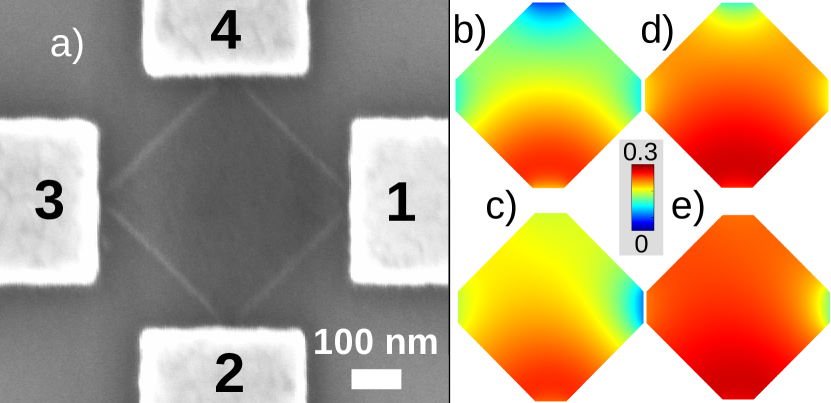
where we assume low frequency limit relevant to our experiments. Our sample, shown in Fig. 1 (a), has four terminals, which are the metallic leads attached to the corners of the box.
One can derive a very general expression Blanter and Büttiker (2000) for the cross correlation (Eq. 1) in terms of the scattering matrix of the device . For practical calculations we use an alternative approach based on the solution of Boltzmann-Langevin equation for diffusive electrons inside the box Blanter and Büttiker (1997); Sukhorukov and Loss (1999), which we outline in the next subsection. The two approaches are equivalent because the scattering matrix can be expressed in terms of the electronic retarded () and advanced () Green’s functions and transmission probabilities of the conducting channels of the terminals Fisher and Lee (1981). Performing disorder averaging of the products in the diffusive conductor with the aid of the standard rules Aleiner et al. (2002), one can reduce the evaluation of the cross correlations (Eq. 1) to the solution of the diffusion equation.
Here our main focus is the HBT exchange effect which is probed by measuring the cross correlation of the currents in terminals 1 and 3, denoted by . The correlations are measured in three DC biasing configurations, namely A, B and C. In A (B) configuration terminal 2 (4) is biased with voltage V while the other three terminals are grounded. In C configuration both terminals 2 and 4 are biased, while 1 and 3 are grounded. The measured current-current cross correlations are negative, but we follow the notation used in Ref. Blanter and Büttiker (2000) which has positive sign. Finally, we consider the difference
| (2) |
By obtaining the exchange correction factor from the measured electronic shot noise, our measurement essentially repeats the original HBT experiment performed with photons R. Hanbury Brown and Twiss (1956). For distinguishable non-interacting particles the noises coming from different sources are additive and the combination (Eq. 2) equals to zero (). However, since the electrons are indistinguishable and obey Fermi statistics one finds that . In theory the cross correlation is given by the sum of partial contributions containing the combinations of the distribution functions in the leads of the form , . The non-zero HBT exchange correction in Eq. (2) originates from the contribution having the form Blanter and Büttiker (1997)
| (3) | |||||
Bias configurations A and B produce the same value for , while it vanishes in the bias configuration C and at zero temperature due to the Pauli principle. Indeed, in this case one finds since , where is the Heaviside step function. Thus, at zero temperature one obtains Blanter and Büttiker (1997)
| (4) | |||||
Here the angular brackets denote averaging over disorder in the diffusive conductor. The HBT exchange correction (Eqs. 2 and 4) can be either positive or negative depending on the system parameters.
As we have mentioned earlier, after disorder averaging quantum interference effects vanish from the HBT exchange noise (Eq. 4). However, from mathematical point of view one can still consider it as a classical interference effect for the distribution function of electrons. Indeed, the distribution function inside the graphene box is the linear combination of the distribution functions in the terminals, see Eq. (5), while the noise cross correlation is the quadratic function of it. It is well known that the original HBT experiment R. Hanbury Brown and Twiss (1956) can also be interpreted in terms of the interference of classical waves. The interpretation of our experiment as analogy to optical interference is discussed further in Sec. VI.
II.1 Semiclassical analysis
The non-equilibrium electron transport can be described by Boltzmann-Langevin approach, Sukhorukov and Loss (1998, 1999) that provides a simple and transparent interpretation of the theory. In this section we provide a brief summary of this approach and derive explicit expressions for the noise cross-correlations in terms of measurable parameters. We account for the effect of finite contact resistances and consider the two regimes – the regime of the elastic transport and the hot electron regime, in which electron-electron interaction leads to thermalization of the electrons and a local electronic temperature can be defined.
Considering the elastic transport regime, in which the electron-electron Coulomb interaction can be ignored, one obtains the solution of the Boltzmann equation for the electron distribution function in the form
| (5) |
where denotes the potential distribution in a diffusive multiterminal conductor corresponding to the bias condition .
The noise correlations can be expressed in terms of a function which describes the non-equilibrium state of the biased multiterminal conductor:
| (6) |
If only one terminal is biased, the function simplifies to in the limit . With two bias voltages, for example at terminals 2 and 4, one obtains . Note that the non-linear dependence of the distribution function () is carried over to dependence on the characteristic function (). Figs. 1 (b,c) display the numerically calculated -functions for a graphene box where the contacts are placed in the corners of the box and their effective width is taken as 20% of the side length . The shape of the function characterizes the diffusion of electrons governed by quantum statistics of fermions.
The noise currents in each terminal can be obtained by integrating the function. For example, the expression for the noise cross-correlations in a graphene box with perfect contacts reads
| (7) |
where is the sheet resistance of graphene. In our experimental configuration with finite contact resistances exhibit jumps across the contacts, which reflect finite voltage drops on them. The effect of the contacts on the noise cross-correlations is discussed below.
One can use the elastic approximation for the electron transport if the escape time of an electron out of the graphene quantum dot, , is much shorter than the electron-electron energy relaxation time , i.e. if . In the opposite case, , hot electron regime becomes relevant. The time is given by the expression
| (8) |
where is the resistance quantum, are the contact resistances and is the level spacing in the square graphene dot,
| (9) |
Here m/s is the speed of electrons in graphene and is the Fermi wave vector. The electron-electron relaxation time is estimated as Voutilainen et al. (2011),
| (10) |
where is the average effective temperature of electrons inside the graphene box. The temperature equals to the bath temperature at low bias voltages applied to the contacts and may grow to higher values in the hot electron regime. For the parameters of our sample listed in Tab. 1 we find that the times (Eqs. 8 and 10) weakly depend on the gate voltage. The escape time approximately takes the value ps, while the electron-electron relaxation time (Eq. 10) may change from ps at the bath temperature mK to much shorter values at high bias. Thus we expect our sample to be in an intermediate regime between ballistic and hot electron transport.
In presence of the inelastic electron-electron scattering the shape of the -function changes. The kinetic equation for the distribution function can be relatively easily found in the hot electron regime , where is the electron-phonon relaxation time. In this regime the electron distribution function has the equilibrium Fermi-Dirac form with coordinate dependent electron temperature, which differs from the temperature of the substrate.
The function (Eq. 6) can be expressed in terms of the characteristic functions both in the elastic and the hot electron regimes. Performing this analysis and generalizing the expression (Eq. 7) to case of finite contact resistances, we derive explicit expressions for the cross-correlation of the noises in terms of the experimentally measurable parameters. Assuming that the electron transport is fully elastic and considering low temperature (or high bias) limit relevant to our experiment, we find
| (11) |
Here are the elements of the conductance matrix, which describe the combined effect of all contact resistances and the inner part of the graphene box, are contact resistances, and are the local noise sources of the contacts evaluated under the assumption of fixed potential of the graphene box. The latter have the form
| (12) | |||||
Here is the Fano factor of the -th contact. The integral in the last term of Eq. (11) runs over the inner part of the graphene box excluding the corner areas, to which the metallic leads are attached.
In the hot electron regime and for the cross-correlation takes the form
| (13) | |||||
Here is the coordinate dependent electronic temperature inside the graphene box given by the expression
| (14) |
are again the local junction noise sources, which now take the form
| (15) | |||||
and are the electronic temperatures inside the box close to the contacts,
| (16) |
II.2 Conductance
As described above, the conductances of graphene and contacts are parameters in our numerical noise model. Therefore, we use the measured conductances shown in Fig. 2 (a,b,d) as a starting point for the numerical noise calculations.

The measured conductances are used to construct a 4-by-4 conductance matrix for the whole system () which is then divided to central graphene part () with uniform conductivity and contact resistances (diagonal matrix ), satisfying . The division is illustrated in Fig. 2 (c). Since the magnitude of graphene resistance in this division is largely arbitrary, the graphene resistance value is based on theoretical sheet conductivity at given gate voltage value. The resistances are listed in Table 1.
| V | 1.39 k | 1.50 k | 1.66 k | 5.38 k | 1.65 k |
|---|---|---|---|---|---|
| V | 1.59 k | 4.47 k | 8.00 k | 36.4 k | 3.70 k |
It can be seen that the contacts 1-3 have comparable resistances far from the CNP while contact 4 has higher resistance. The differences between the contacts become more significant when approaching the CNP.
The relatively high contact resistances () are to a large extent explained by narrow regions in the graphene, which can be thought as graphene nanoconstrictions Terrés et al. (2016); Krishna Kumar et al. (2017); Clericò et al. (2018). Therefore, their effect is briefly studied below. The conductance of such nanoconstriction is given by:
| (17) |
where is related to edge roughness ( for rough edges), is the width of the constriction and is the Fermi wave vector in graphene. For 300 nm gate oxide , where is the gate voltage corresponding to the charge neutrality point Das Sarma et al. (2011).
The blue curve in Fig. 2 (d) shows the measured conductance as a function of gate voltage between terminals 1 and 3 (with 2 and 4 floating, i.e. ) and fit to the constriction model (Eq. 17) as , where the resistance of the central region, , contributes by 50 % to the total resistance (far from CNP) according to our conductance model. In the calculation we use nm (estimated from SEM image) and set the value of to its theoretical value. Good agreement is found by setting the edge roughness parameter , which is close to the previously reported experimental values 0.56 Terrés et al. (2016) and 0.74 Clericò et al. (2018). One may also deduce the number of conduction channels in the contacts (), which becomes 7 far from CNP ( V) and 3 near it ( V) in our device. However, it should be noted that the presence of increased carrier density due to proximity of metallic contacts can increase , leading to smaller , and therefore the obtained parameter values are only estimates. Also, here we assume , ignoring possible other contributions to contact resistance. We note that the non-zero conductance near the CNP is most probably caused by doping from contacts and impurities.
II.3 Numerical calculations
We base our numerical calculations on the coherent and hot electron models described above. While the contact contributions are readily obtainable from the first terms of Eqs. (11) and (13), the graphene terms are calculated numerically. We find the four characteristic functions by numerically solving 111Comsol Multiphysics was used for the calculation. the diffusion equation in a 2D geometry representing the graphene box. The chamfered corner terminals (width 20 % of box edge) have a constant voltage by setting (for ) for the whole system, and subtracting the voltage drop in each contact, calculated using and . Thus the corner terminals have Dirichlet boundary condition while the box edges have zero perpendicular flux (Neumann boundary). The values of (for ) and (for ) are evaluated in a grid for numerical integration.
We obtain the noise cross-correlations in bias configurations A, B and C (denoted by ) and equivalently the autocorrelations and , which are denoted by . To compare the calculated and measured results more easily we introduce a dimensionless scaled exchange factor (and similarly ). Both quantities are calculated far from CNP (at V) and near it (at V, while V). The contact Fano factors turn out to have only little effect on the end result, and hence we set ; equivalent results are obtained even with values approaching the quantum point contact limit (). Since the applied bias is relatively large, we can use the assumption in the hot electron regime.
The calculated distributions of the function in bias configuration A (and equivalent temperature for hot electron regime) are presented in Fig. 1 (b–e). It can be seen that the distribution concentrates near the biasing terminal in the coherent regime (b,c) while more uniform distributions are observed in the hot electron regime (d,e). The increased asymmetry of contact resistances near the CNP (c,e) is also reflected to the noise distributions.
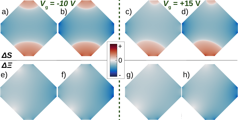
The distributions of the exchange factors and are shown in Fig. 3. The integrated values of the these quantities are negative, although the distributions of have positive contribution near the biasing contacts 2 and 4, where . The low conductance of contact 4 reduces the size of the positive region near it, and increased conductance asymmetry at V also clearly increases the asymmetry in the distributions. In general, the difference between the coherent and hot electron regimes appears as small change in the overall level, although the integrated values show larger difference. The values of are negative over the whole box, and the distributions are slightly concentrated towards the probing terminal 1 (on the right).
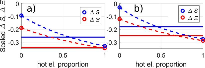
The calculated and including the contact and graphene contributions in coherent and hot electron regimes are plotted in Fig. 4 (a) and (b) for far and near the CNP, respectively. The exchange factors are plotted as a function of hot electron proportion: the coherent result is on the left end and hot electron result on the right with a crossover regime between the two extremes. It can be seen that the coherent model results in too weak exchange factors compared to the experiment, while hot electron regime produces too strong . Since the experimental results fall between the two regimes, we approximate the coherent - hot electron crossover regime by applying linear interpolation as a function of hot electron contribution to calculated cross- and autocorrelations ( and ) individually and calculate the resulting exchange factors which are shown as dashed lines in Fig. 4. A relatively good agreement is obtained at % hot electron contribution at V and % at V. It should be noted, however, that such interpolation only provides a rough estimate of the behavior in the crossover regime.
III Experimental methods
The sample (see Fig. 1 (a)) is fabricated from micromechanically cleaved graphene on heavily p-doped substrate with 300 nm gate oxide. The graphene extends under the Cr/Au contact electrodes. The bonding pads are sufficiently small () so that only 10 % of noise is shunted capacitively to the back-gate electrode.
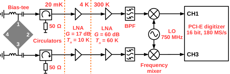
A schematic of the experimental setup is shown in Fig. 5. The experiments are conducted on a BlueFors dry dilution refrigerator at 20 mK. The sample is connected to two high-frequency measurement channels with bias-tees separating the DC and RF paths. Both channels have home-made HEMT low-noise amplifiers (LNA) mounted at 4 K stage Nieminen et al. (2016) reaching system noise temperatures of 10 K for channel 1 and 15 K for channel 3. After additional amplification and band-pass filtering (BPF) in room temperature the RF signal is mixed down with a local oscillator (LO) at 750 MHz and digitized at 180 megasamples per second (MS/s) with AlazarTech ATS9642 digitizer connected to PCI-E bus of a desktop computer. The cross- and autocorrelations are calculated from the digitized data using graphics processing unit (GPU) acceleration. Noise power coupling issues were treated along the lines given in Ref. Danneau et al. (2008b).
IV Results
Our cross-correlation results for the HBT exchange term are displayed in Fig. 6 (a) on the plane spanned by the gate () and bias () voltages; the Dirac point is located around V. At small bias, we observe a clear negative HBT effect; as expected for fermionic diffusion, the signal grows linearly with the bias voltage . A suppression of noise due to the interference of mutually incoherent electrons has been observed in an experiment with a ballistic electron beam splitter Liu et al. (1998). Our results demonstrate that this effect is also observable in mesoscopic diffusive conductors.
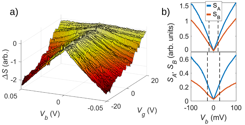
The value for scaled was calculated by making linear fits to the measured noise cross-correlation vs. bias voltage at and mV for V. The lower conductance near the CNP increases the variance of the data, and therefore a wider range of between mV is used for V. The data are linear within those intervals, as shown in Fig. 6 (b), although some deviation emerges when approaching the Dirac point due to lower conductance. The use of smaller intervals in fitting increased the variance of the resulting due to statistical errors, but the average values remained the same. Therefore, our fits can be considered as small-bias extrapolation to zero bias. We calculate the exchange factors for negative and positive separately to see the scattering of the data.
The determined as a function of gate voltage is shown in Fig. 7 (a) together with numerical results of the coherent and hot electron models ( V) and close to ( V) the CNP. The data are scattered mainly due to statistical errors, although a clear trend in can be seen: the effect stays rather constant between and tends linearly towards zero when approaching the Dirac point. The increased scattering of the data at large is due to smaller absolute values of noise, as seen in Fig. 6, and resulting statistical error.
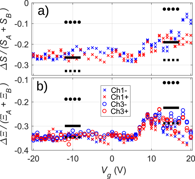
In addition to cross-correlations, we determined the scaled exchange factors for the measured noise in individual channels (autocorrelation). The obtained are shown in Fig. 7 (b) together with the results of the numerical model. shows similar constant behavior below V as , but the slope approaching the CNP is steeper and the scattering near CNP is significant.
When comparing the experimentally determined exchange factors to the results from diffusive calculations described in Sec. II.3, it can be seen that the experimental values are situated between the coherent and hot electron results (black lines dashed with circles and squares, respectively, in Fig. 7). For autocorrelation, the experimental results agree well with the hot electron model, but for cross-correlation the hot electron model results in too strong HBT exhange effect. For best overall agreement, we obtain linearly interpolated values in the crossover regime (see Fig. 4) with 60 % hot electron contribution far from CNP and 50 % close the CNP. The interpolated values are shown as solid black lines in Fig. 7. As already mentioned, however, such linear interpolation gives an inadequate picture of the crossover regime, and therefore the interpolated values should only be considered as rough estimates.
V Discussion
There are several ways to construct a model for a graphene box. One of the simplest is the chaotic quantum dot described by a single distribution function van Langen and Büttiker (1997). A straightforward generalization of this model is to adopt the semiclassical model and to describe the graphene using a single distribution function governed by contact resistances with an arbitrary Fano factor. This model is in fact quite close to the model employed in Ref. Tan et al. (2018). Such a model, lacking voltage variation over the graphene box, was not able to match all the measured quantities , , , properly. First after inclusion of the characteristic potential distributions, a satisfactory agreement could be achieved.
Closest to the present work is our previous experiment with a graphene cross sample with 50 nm nanoribbon arms Tan et al. (2018). In that graphene cross the HBT effect was characterized by occupation number noise in the nearly ballistic central region and regular diffusive noise in the ribbon arms. The HBT effect far from CNP in the cross sample () is of comparable magnitude as in the box (), while the HBT effect near the CNP was strongly enhanced in the cross sample (to ) but is suppressed in the graphene box. This is in line with the theoretical findings Blanter and Büttiker (1997) that geometrical details of the sample strongly affect the observed HBT exchange effect.
The shot noise in our sample is generated in the central graphene region, as well as the narrow constrictions at the contacts contributing significantly to sample resistance (see Eq. 11). The contact resistances affect the characteristic potential distribution in the central region, and thus also their asymmetry has significant effect on the noise. We note that, for such small contacts as we have in our sample, the contact capacitance can be regarded negligible (on the basis of Ref. Laitinen et al. (2016)), and the reactive impedance part at the noise measurement frequency does not bypass the contact resistance, resulting that the DC conductance values are sufficient for the noise circuit analysis.
The fact that the Dirac point in our sample is not well defined (see Figs. 2 and 7) indicates presence of nonuniform doping, possibly due to contributions from fabrication residues, proximity of the contacts, and localized states at the edges. These locally varying doping effects would lead to nonuniform conductance in the regime of charge puddles near the Dirac point. Nonuniform conductance can easily be implemented in our numerical calculations, but this approach was not found exceedingly beneficial, and was given up due to further increase in the already high number of our fitting parameters. In addition, the characteristic statistics of the charge puddles are unknown, making it impossible to justify any specific configuration of non-uniformity in our model.
According to Fig. 7, our results are intermediate between coherent and hot electron transport. Theoretically, however, the strength of electron-electron interactions grows as due to the increase in the available scattering states with bias voltage. Therefore, we would expect the electron propagation in our graphene box transform gradually with bias even closer to hot electron regime with decreasing electron-electron scattering length Nagaev (1995). Instead of an increase in the shot noise due to hot electron effects, we find a 5% decrease in total () at mV compared with the value deduced using the low bias Fano factor. This decrease is assigned to inelastic scattering, i.e. to the onset of scattering by polar surface modes in graphene/SiO2 system Chen et al. (2008); Fratini and Guinea (2008). Our experimental results do not show any noticeable change in up to bias voltage mV, and hence pure hot electron regime was not fully achieved in our experiments. The independence of our results on bias at mV, suggests that and might include features inherent to diffusive graphene.
It is instructive to consider the analogy between our experiment and interference experiments in optics. We note that in Eq. (7) the function is multiplied by gradients and . In analogy with optics, these gradients can be interpreted as distributed detector functions ”filtering” the -function. They vary smoothly inside the graphene box, which implies that the whole box acts as an ”interferometer screen”. In this interpretation the noise cross-correlation is given by an area integral weighted with the geometric response functions. For a simple description, we employ an analogy with a double slit experiment where the incoming intensity on the detector is determined in three different configurations: the experiment is performed by closing first one slit (), then the other slit (), and finally by keeping both slits open (); here the applied electric potential is the analogue of light in the double slit experiment. In our case, the ”detection screen” is the whole graphene box where interference due to takes place at every point. The recorded interference value is an integral provided by the cross correlation measurements (see Eq. 7) where we take the equivalent of (the difference between the actual interference pattern and the two backgrounds), namely . Although, this analogue is illuminating for understanding the setting of our experiment, the underlying effects are two-particle interferences. The correlation effects arise via the competition of the available states in the reservoirs for the outgoing electrons. The non-equilibrium -function (see Fig. 1 (b,c)) carries this information over to the whole sample. However, the actual phase dependence of the two particle scattering events is averaged out in our diffusive conductor Blanter and Büttiker (1997). Due to the lack of phase dependence, we prefer to call our observed results as HBT exchange effects, even though interference by two diffusive wave fronts describes the phenomena in the sense of our analogy.
VI Conclusions
We have studied exchange cross correlations in a disordered graphene box. Our experimental results display distinct Hanbury Brown and Twiss (HBT) exchange correlations, which deviate from the standard predictions of scattering matrix theory. Our results indicate that the finite contact resistances significantly affect the noise cross-correlations in a diffusive system. The values of experimentally determined HBT exchange effects fall between calculated values for coherent and hot electron models, indicating either the presence of bias-independent crossover regime or intrinsic behavior of diffusive graphene which is not captured by standard model for diffusive systems. The overall picture is the same for both near and far from the Dirac point, although the low carrier density near the CNP leads to further deviations between the model and experimental data.
Acknowledgements
We thank Florian Libisch and Stefan Rotter for fruitful discussions. This work was supported by the Academy of Finland projects 314448 (BOLOSE), 310086 (LTnoise) and 312295 (CoE, Quantum Technology Finland) as well as by ERC (grant no. 670743). This research project utilized the Aalto University OtaNano/LTL infrastructure which is part of European Microkelvin Platform. T.E. is grateful to Vilho, Yrjö and Kalle Väisälä Foundation for scholarship. The work of G.B.L. was supported by Aalto University School of Science Visiting Professor grant, the Government of the Russian Federation (Agreement No. 05.Y09.21.0018), by the RFBR Grant No. 17-02-00396A, and Foundation for the Advancement of Theoretical Physics and Mathematics ”BASIS”.
References
- Kogan (1996) S. Kogan, Electronic Noise and Fluctuations in Solids (Cambridge University Press, Cambridge, 1996).
- Blanter and Büttiker (2000) Y. M. Blanter and M. Büttiker, Shot noise in mesoscopic conductors, Phys. Rep. 336, 1 (2000).
- Martin (2005) T. Martin, Noise in mesoscopic physics, in Les Houches Summer Sch. Proc., Vol. 81, edited by H. Bouchiat, Y. Gefen, S. Guéron, G. Montambaux, and J. Dalibard (Elsevier Ltd, 2005) Chap. 5, pp. 283–359.
- Lesovik and Sadovskyy (2011) G. B. Lesovik and I. A. Sadovskyy, Scattering matrix approach to the description of quantum electron transport, Physics-Uspekhi 54, 1007 (2011).
- Liu et al. (1998) R. C. Liu, B. Odom, Y. Yamamoto, and S. Tarucha, Quantum interference in electron collision, Nature 391, 263 (1998).
- Oliver (1999) W. D. Oliver, Hanbury Brown and Twiss-Type Experiment with Electrons, Science 284, 299 (1999).
- Henny et al. (1999) M. Henny, S. Oberholzer, C. Strunk, T. Heinzel, K. Ensslin, M. Holland, and C. Schönenberger, The Fermionic Hanbury Brown and Twiss Experiment, Science 284, 296 (1999).
- Glattli (2005) D. C. Glattli, Tunneling Experiments in the Fractional Quantum Hall Effect Regime, in Quantum Hall Eff. Poincaré Semin. 2004, edited by B. Douçot, V. Pasquier, B. Duplantier, and V. Rivasseau (Birkhäuser Basel, Basel, 2005) pp. 163–197.
- R. Hanbury Brown and Twiss (1956) R. Hanbury Brown and R. Q. Twiss, Correlation between photons in two coherent beams of light, Nature 177, 27 (1956).
- Neder et al. (2007) I. Neder, N. Ofek, Y. Chung, M. Heiblum, D. Mahalu, and V. Umansky, Interference between two indistinguishable electrons from independent sources, Nature 448, 333 (2007).
- Blanter and Büttiker (1997) Y. M. Blanter and M. Büttiker, Shot-noise current-current correlations in multiterminal diffusive conductors, Phys. Rev. B 56, 2127 (1997).
- Sukhorukov and Loss (1999) E. V. Sukhorukov and D. Loss, Noise in multiterminal diffusive conductors: Universality, nonlocality, and exchange effects, Phys. Rev. B 59, 54 (1999).
- Tan et al. (2018) Z. B. Tan, T. Elo, A. Puska, J. Sarkar, P. Lähteenmäki, F. Duerr, C. Gould, L. W. Molenkamp, K. E. Nagaev, and P. J. Hakonen, Hanbury-Brown and Twiss exchange and non-equilibrium-induced correlations in disordered, four-terminal graphene-ribbon conductor, Sci. Rep. 8, 14952 (2018).
- Katsnelson (2006) M. I. Katsnelson, Zitterbewegung, chirality, and minimal conductivity in graphene, Eur. Phys. J. B 51, 157 (2006).
- Tworzydło et al. (2006) J. Tworzydło, B. Trauzettel, M. Titov, A. Rycerz, and C. W. J. Beenakker, Sub-Poissonian Shot Noise in Graphene, Phys. Rev. Lett. 96, 246802 (2006).
- San-Jose et al. (2007) P. San-Jose, E. Prada, and D. S. Golubev, Universal scaling of current fluctuations in disordered graphene, Phys. Rev. B 76, 195445 (2007).
- Lewenkopf et al. (2008) C. H. Lewenkopf, E. R. Mucciolo, and A. H. Castro Neto, Numerical studies of conductivity and Fano factor in disordered graphene, Phys. Rev. B 77, 081410 (2008).
- Laakso and Heikkilä (2008) M. A. Laakso and T. T. Heikkilä, Charge transport in ballistic multiprobe graphene structures, Phys. Rev. B 78, 205420 (2008).
- DiCarlo et al. (2008) L. DiCarlo, J. R. Williams, Y. Zhang, D. T. McClure, and C. M. Marcus, Shot Noise in Graphene, Phys. Rev. Lett. 100, 156801 (2008).
- Danneau et al. (2008a) R. Danneau, F. Wu, M. F. Craciun, S. Russo, M. Y. Tomi, J. Salmilehto, A. F. Morpurgo, and P. J. Hakonen, Shot Noise in Ballistic Graphene, Phys. Rev. Lett. 100, 196802 (2008a).
- Danneau et al. (2009) R. Danneau, F. Wu, M. F. Craciun, S. Russo, M. Y. Tomi, J. Salmilehto, A. F. Morpurgo, and P. J. Hakonen, Shot noise measurements in graphene, Solid State Commun. 149, 1050 (2009).
- Danneau et al. (2010) R. Danneau, F. Wu, M. Y. Tomi, J. B. Oostinga, a. F. Morpurgo, and P. J. Hakonen, Shot noise suppression and hopping conduction in graphene nanoribbons, Phys. Rev. B 82, 161405 (2010).
- Schottky (1918) W. Schottky, Über spontane Stromschwankungen in verschiedenen Elektrizitätsleitern, Ann. Phys. 57, 541 (1918).
- Khlus (1987) V. A. Khlus, Current and voltage fluctuations in microjunctions between normal metals and superconductors, Sov. Phys JETP 66, 1243 (1987).
- Landauer (1989) R. Landauer, Johnson-Nyquist noise derived from quantum mechanical transmission, Phys. D 38, 226 (1989).
- Lesovik (1989) G. B. Lesovik, Excess quantum noise in 2D ballistic point contacts, JETP Lett. 49, 592 (1989).
- Yurke and Kochanski (1990) B. Yurke and G. P. Kochanski, Momentum noise in vacuum tunneling transducers, Phys. Rev. B 41, 8184 (1990).
- Büttiker (1990) M. Büttiker, Scattering theory of thermal and excess noise in open conductors, Phys. Rev. Lett. 65, 2901 (1990).
- Beenakker and Büttiker (1992) C. W. J. Beenakker and M. Büttiker, Suppression of shot noise in metallic diffusive conductors, Phys. Rev. B 46, 1889 (1992).
- Nagaev (1992) K. Nagaev, On the shot noise in dirty metal contacts, Phys. Lett. A 169, 103 (1992).
- Fisher and Lee (1981) D. S. Fisher and P. A. Lee, Relation between conductivity and transmission matrix, Phys. Rev. B 23, 6851 (1981).
- Aleiner et al. (2002) I. Aleiner, P. Brouwer, and L. Glazman, Quantum effects in Coulomb blockade, Phys. Rep. 358, 309 (2002).
- Sukhorukov and Loss (1998) E. V. Sukhorukov and D. Loss, Universality of Shot Noise in Multiterminal Diffusive Conductors, Phys. Rev. Lett. 80, 4959 (1998).
- Voutilainen et al. (2011) J. Voutilainen, A. Fay, P. Häkkinen, J. K. Viljas, T. T. Heikkilä, and P. J. Hakonen, Energy relaxation in graphene and its measurement with supercurrent, Phys. Rev. B 84, 045419 (2011).
- Terrés et al. (2016) B. Terrés, L. A. Chizhova, F. Libisch, J. Peiro, D. Jörger, S. Engels, A. Girschik, K. Watanabe, T. Taniguchi, S. V. Rotkin, J. Burgdörfer, and C. Stampfer, Size quantization of Dirac fermions in graphene constrictions, Nat. Commun. 7, 11528 (2016).
- Krishna Kumar et al. (2017) R. Krishna Kumar, D. A. Bandurin, F. M. Pellegrino, Y. Cao, A. Principi, H. Guo, G. H. Auton, M. Ben Shalom, L. A. Ponomarenko, G. Falkovich, K. Watanabe, T. Taniguchi, I. V. Grigorieva, L. S. Levitov, M. Polini, and A. K. Geim, Superballistic flow of viscous electron fluid through graphene constrictions, Nat. Phys. 13, 1182 (2017).
- Clericò et al. (2018) V. Clericò, J. A. Delgado-Notario, M. Saiz-Bretín, C. Hernández Fuentevilla, A. V. Malyshev, J. D. Lejarreta, E. Diez, and F. Domínguez-Adame, Quantized Electron Transport Through Graphene Nanoconstrictions, Phys. Status Solidi 215, 1701065 (2018).
- Das Sarma et al. (2011) S. Das Sarma, S. Adam, E. H. Hwang, and E. Rossi, Electronic transport in two-dimensional graphene, Rev. Mod. Phys. 83, 407 (2011).
- Note (1) Comsol Multiphysics was used for the calculation.
- Nieminen et al. (2016) T. Nieminen, P. Lähteenmäki, Z. Tan, D. Cox, and P. J. Hakonen, Low-noise correlation measurements based on software-defined-radio receivers and cooled microwave amplifiers, Rev. Sci. Instrum. 87, 114706 (2016).
- Danneau et al. (2008b) R. Danneau, F. Wu, M. F. Craciun, S. Russo, M. Y. Tomi, J. Salmilehto, A. F. Morpurgo, and P. J. Hakonen, Evanescent Wave Transport and Shot Noise in Graphene: Ballistic Regime and Effect of Disorder, J. Low Temp. Phys. 153, 374 (2008b).
- van Langen and Büttiker (1997) S. A. van Langen and M. Büttiker, Quantum-statistical current correlations in multilead chaotic cavities, Phys. Rev. B 56, R1680 (1997).
- Laitinen et al. (2016) A. Laitinen, G. S. Paraoanu, M. Oksanen, M. F. Craciun, S. Russo, E. Sonin, and P. Hakonen, Contact doping, Klein tunneling, and asymmetry of shot noise in suspended graphene, Phys. Rev. B 93, 1 (2016).
- Nagaev (1995) K. E. Nagaev, Influence of electron-electron scattering on shot noise in diffusive contacts, Phys. Rev. B 52, 4740 (1995).
- Chen et al. (2008) J.-H. Chen, C. Jang, S. Xiao, M. Ishigami, and M. S. Fuhrer, Intrinsic and extrinsic performance limits of graphene devices on SiO2, Nat. Nanotechnol. 3, 206 (2008).
- Fratini and Guinea (2008) S. Fratini and F. Guinea, Substrate-limited electron dynamics in graphene, Phys. Rev. B 77, 195415 (2008).