Intrinsic photon loss at the interface of superconducting devices
Abstract
We present a quantum theory of dielectric energy loss arising from the piezoelectric coupling between photons and phonons in superconducting devices. Photon loss is shown to occur predominantly at the interface, where the piezoelectric effect is non-zero even when the materials are perfectly crystalline (epitaxial) and free of two-level system defects. We present explicit numerical calculations for the value of the intrinsic loss tangent at several interfaces to conclude that the of superconducting qubits may reach over s if the device is made with defect-free interfaces.
Qubits based on Josephson junctions have come a long way and became one of the most promising devices for quantum information processing. Although coherence times have improved by several orders of magnitude in the past two decades Devoret and Schoelkopf (2013), relatively short coherence is still arguably the main obstacle in the implementation of large scale quantum computation.
Coherence times in state-of-the-art Josephson devices are limited by energy relaxation ( decay) Rigetti et al. (2012); Nguyen et al. (2019); Place et al. and there are many noise/relaxation sources that can play a role. Understanding the physical origin of these sources is key to make further progress on coherence times. While any excitation with electric dipole moment can contribute to electric (photon) energy loss, a large number of experiments with superconducting resonators provide evidence of loss dominated by extrinsic sources that can be modelled as a bath of two-level-systems (TLSs) Martinis et al. (2005); Shalibo et al. (2010); Grabovskij et al. (2012); Khalil et al. (2014); Skacel et al. (2015); Lisenfeld et al. (2016); Sarabi et al. (2016); Romanenko and Schuster (2017). The evidence for TLSs is based on the observation that the loss tangent (proportional to the inverse quality factor of the circuit, ) always decreases with increasing microwave power, and this can only be explained by TLS saturation. At high power, when TLSs are saturated, the origin of the residual loss is not understood Skacel et al. (2015).
An additional mechanism of loss is phonon radiation due to the piezoelectric effect O’Connell et al. (2010). It is well known that Josephson junctions radiate phonons at the Josephson frequency, but it is still not clear whether this occurs due to presence of TLSs or due to the piezoelectric effect Berberich et al. (1982). Ioffe et al. Ioffe et al. (2004) proposed a mechanism of phonon radiation due to piezoelectricity in disordered junctions; assuming the qubit electrical energy was mostly concentrated at the Josephson junction and a rough estimate using bulk material parameters led to the conclusion that this effect could be responsible for the typical observed in superconducting qubits Ioffe et al. (2004). However, systematic studies of qubit relaxation for varying qubit geometries showed that was proportional to the electrical energy at the interfaces away from the Josephson junction Wang et al. (2015); Dial et al. (2016). In spite of its ubiquity, the contribution of piezoelectricity to the quality factor of superconducting qubits is not known.
In this Letter we describe a quantum theory of photons and phonons coupled by the piezoelectric effect. In the microwave range the resulting loss is ineffective in large bulk piezoelectric materials. However, the loss is found to be greatly enhanced at piezoelectric substrates with finite thickness, as well as surfaces and interfaces of non-piezoelectric materials, where material discontinuity generally leads to piezoelectricity. As a result, dielectric loss due to phonon radiation is an intrinsic effect, that is present even when the surfaces, interfaces, and substrates are perfect crystals.
Quantum theory of photons and phonons coupled by the piezoelectric effect.– When a photon travels inside an insulator it inevitably has finite lifetime, in that the pure photon is no longer an eigenstate of the material’s Hamiltonian. This occurs because the material has excitations and defects with electric dipole moment. The coupling is most effective when the frequency of the photon is resonant with the frequencies of the excitations contributing to the material’s polarization (electric dipole moment per volume). In the microwave range a large density of acoustic phonons always satisfies these conditions; the phonons acquire electric dipole moment whenever the material or device lacks inversion symmetry, e.g. due to the presence of an interface or disorder.
As a starting point, we take a single photon mode as the representative for electrical energy stored in a quantum device. Later we generalize to many modes and arbitrary electrical energy distribution. The Hamiltonian for photon plus phonons is given by
| (1) |
where the operator creates a photon with frequency , and the operator creates an acoustic phonon with wavevector and frequency , with the phonon velocity. The photon electric field operator
| (2) |
is written in terms of the photon shape vector which is normalized to the photon volume, . The constant is the microwave frequency dielectric constant, which arises from non-resonant mechanisms such as electronic and optical phonon excitations.
Due to piezoelectricity the phonon electric polarization becomes approximately proportional to the divergence of the phonon displacement operator, Snoke (2020). The constant of proportionality is denoted “piezoelectric vector”; as shown in Sup this is a function of the coefficients of the piezoelectric tensor. Here is assumed to depend on position in order to describe inhomogeneous systems such as interfaces and junctions. Inserting the usual expression for phonon displacement we get
| (3) |
where is the volume of the insulator (e.g. the dielectric substrate, which is assumed to be different than , the volume of the photon mode), and is its mass density. Note that has the same dimensions as , charge/area, and by symmetry it points perpendicular to an interface.
The interaction between photons and phonons is given by
| (4) | |||||
with coupling amplitude
| (5) |
In Eq. (4) we neglected terms such as and , because they can’t conserve energy so they don’t contribute to energy loss. The terms that conserve total energy lead to energy dissipation for the photon system, with rate given by
| (6) |
where is the rate for processes that convert a photon into a phonon (energy loss), with the opposite process of energy gain. The former and the latter are induced by the terms and in Eq. (4), respectively. Using Fermi’s golden rule we get
| (7) |
where and are the number of photons in mode and the number of phonons in mode , respectively. The expression for is obtained by replacing for .
Plugging the amplitudes (5) into Eqs. (6) and (7) leads to a general expression for the inverse quality factor , which is the fractional energy lost per cycle:
| (8) | |||||
where we assumed the phonons are at thermal equilibrium at some temperature , i.e. their occupation is equal to the Bose distribution . If in addition the photon system is also at thermal equilibrium, will also be equal to and Eq. (8) will become exactly equal to zero. This shows that Eq. (8) satisfies detailed balance.
It is straightforward to generalize Eq. (8) to an arbitrary number of photon modes. The final answer is to replace by , where is the space-dependent electric field (a classical field).
Key role of photon confinement.– Consider a bulk piezoelectric material so that and assume that points along some direction in the crystal with constant. In this case the photons can be regarded as plane waves, , and Eq. (5) is non-zero only for phonons with (conservation of momentum). Since Eq. (7) requires conservation of energy ( or ), it yields for . Therefore, the piezoelectric mechanism yields zero dissipation in bulk.
Now consider what happens in a piezoelectric substrate with large area , but finite thickness . In this case we have , where is the Heaviside step function and is the unit vector perpendicular to plane . The photon shape function is assumed to be , with photon propagation wavevector perpendicular to . Now the phonon-photon momentum conservation in Eq. (5) is reduced to , with arbitrary. This freedom allows satisfaction of energy conservation with , where () denotes a phonon emitted along (). These considerations allow exact evaluation of Eq. (8), leading to . The prefactor is the fraction of total electrical energy at the substrate, denoted participation ratio Wang et al. (2015), and the intrinsic loss tangent for the substrate is given by
| (9) |
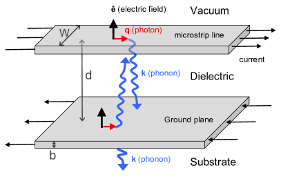
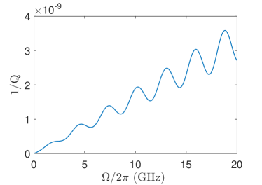
Note how this is proportional to , so it goes to zero in the bulk limit: When either or is large enough so that the phonon wavelength is much smaller than , . Moreover, Eq. (9) is oscillatory as a function of and . This is a consequence of phonon interference. This interference, being unique to the piezoelectric mechanism, offers a way to distinguish it from other sources such as extrinsic loss due to TLSs. However, the interference averages out when varies on the scale of ( m for GHz). In the case of spatial variations the sine squared in Eq. (9) averages to and we denote the loss tangent by . The washing out of the interference can be avoided in other geometries such as the stripline which we explore to give a clear signature of the intrinsic piezoelectricity, see Fig. 1(a).
| Metal/Vacuum | (Å) | (C/m2) | Reference |
| Al | Calculated in Sup | ||
| Nb | Calculated in Sup | ||
| Dielectric/Vacuum | |||
| Al2O3 | First-principles Georgescu and Ismail-Beigi (2019) | ||
| Dielectric/Metal | |||
| Al2O3/Al | Calculated in Sup | ||
| Substrate | (Å) | (C/m2) | |
| SiO2 | Measured in Tarumi et al. (2007) | ||
| Nb2O5 | Estimated |
Now consider what happens at the surface or interface of non-piezoelectric materials (with ). The photon electric field induces a screening areal charge density, which changes the effective charge of interface atoms. As a result the materials are subject to extra electric stress within a length scale , the surface/interface thickness. A simple calculation Sup yields , with the unit vector perpendicular to the interface (pointing from material 1 to 2), and depending on the type of surface/interface as shown in Table 1.
Explicit calculation of Eq. (8) for and leads to , where and are the participation ratio and intrinsic loss tangent for the interface,
| (10) |
The last factor in Eq. (10) contains parameters for the two interface materials (). This happens because the phonon propagating along () moves into material 2 (1).
| Junctions | |
|---|---|
| Al/Al2O3/Al | |
| Nb/Nb2O5/Nb | |
| Metal/Vacuum | |
| Al | |
| Nb | |
| Dielectric/Vacuum | |
| Al2O3 | |
| Dielectric/Metal | |
| Al2O3/Al | |
| Substrate | |
| SiO2 | |
| Nb2O5 |
For a small Josephson junction with lateral size we may approximate and in Eq. (8) leading to , with
| (11) |
where is the volume of the junction. This expression contains an additional prefactor of when compared to the result obtained in Ioffe et al. (2004).
Table 2 shows explicit calculations of Eq. (10) for epitaxial junctions, interfaces, and substrates, assuming GHz, mK, , and material parameters described in Sup . The table shows a factor of decrease in loss tangent can be obtained if the extrinsic mechanism due to interface TLSs is suppressed.
For more complex devices with multiple interfaces and junctions such as qubits, one can use to denote the participation ratio in each region . The contribution from dielectric loss to the rate for energy relaxation of a qubit with ground and excited state becomes
| (12) |
where is the qubit Hamiltonian, and are its capacitance and associated charge operator, and is the loss tangent calculated from Eqs. (9)–(11). For weakly nonlinear oscillators such as transmons, Eq. (12) reduces to the well known expression when Wang et al. (2015); Sup .
Phonon interference as the experimental signature of the intrinsic piezoelectric effect.– For devices with interfaces separated by a distance of the order of the phonon wavelength ( m for GHz), the phonons emitted by the interface piezoelectric effect will show signatures of interference. Consider the microstrip line shown in Fig. 1a; it can be modelled by equal to a sum of delta functions at each interface. Explicit calculations of Eq. (8) show that the loss tangent becomes oscillatory as a function of frequency for interface separation , see Fig. 1b. The loss tangent is also oscillatory as a function of . These oscillations can be used to distinguish the interface piezoelectric mechanism from other sources such as extrinsic loss due to TLSs. In the presence of other sources, the amplitude of the oscillations will be diminished. The period of the oscillations is approximately MHz, so they can be detected with quite small frequency detunings in millimeter sized microwave devices Paik et al. (2011); Wang et al. (2015).
Conclusions.– We presented a theory of photon loss due to the piezoelectric effect. Our main result is Eq. (8), the explicit expression for the fraction of photon loss per cycle () in a general inhomogeneous structure.
We showed that piezoelectric loss does not occur in bulk materials, it only occurs in the presence of photon confinement. This includes piezoelectric substrates with finite thickness (or equivalently finite photon penetration depth), as well as interfaces and junctions made of materials that are non-piezoelectric in the bulk.
In current devices, photon loss is dominated by the presence of extrinsic TLS defects with localized dipole moment. Substantial effort is underway Place et al. to make devices with epitaxial interfaces, free of TLS defects. For these perfect devices, piezoelectricity provides the ultimate loss mechanism: Even perfect interfaces made of non-piezoelectric materials become piezoelectric because of inversion symmetry breaking. Table 2 shows explicit numerical predictions of the intrinsic loss tangent in several different crystalline junctions, interfaces, and substrates.
Using typical transmon qubit participation ratios , , and (design A from Wang et al. (2015)) we predict that a device made of epitaxial aluminum and sapphire will attain at GHz, with most of the loss occurring at the aluminum/vacuum surface. Therefore, superconducting qubits with optimal interfaces can reach up to s, above the threshold for quantum error correction Devoret and Schoelkopf (2013). Even longer can be reached for the fluxonium qubit Nguyen et al. (2019); Lin et al. (2018); Earnest et al. (2018) whose design minimizes the quantum matrix element appearing in Eq. (12).
Acknowledgements.
We acknowledge financial support from NSERC (Canada) through its Discovery (RGPIN-2015-03938) and Collaborative Research and Development programs (CRDPJ 478366-14). We thank M. H. Amin, A. N. Cleland, T. Lanting, M. Mariantoni, T. Juginger, and T. Tiedje for useful discussions.References
- Devoret and Schoelkopf (2013) M. H. Devoret and R. J. Schoelkopf, Science 339, 1169 (2013).
- Rigetti et al. (2012) C. Rigetti, J. M. Gambetta, S. Poletto, B. L. T. Plourde, J. M. Chow, A. D. Córcoles, J. A. Smolin, S. T. Merkel, J. R. Rozen, G. A. Keefe, M. B. Rothwell, M. B. Ketchen, and M. Steffen, Phys. Rev. B 86, 100506 (2012).
- Nguyen et al. (2019) L. B. Nguyen, Y. H. Lin, A. Somoroff, R. Mencia, N. Grabon, and V. E. Manucharyan, Phys. Rev. X 9, 041041 (2019).
- (4) A. P. M. Place, L. V. H. Rodgers, P. Mundada, B. M. Smitham, M. Fitzpatrick, Z. Leng, A. Premkumar, J. Bryon, S. Sussman, G. Cheng, T. Madhavan, H. K. Babla, B. Jaeck, A. Gyenis, N. Yao, R. J. Cava, N. P. de Leon, and A. A. Houck, arXiv:2003.00024 .
- Martinis et al. (2005) J. M. Martinis, K. B. Cooper, R. McDermott, M. Steffen, M. Ansmann, K. D. Osborn, K. Cicak, S. Oh, D. P. Pappas, R. W. Simmonds, and C. C. Yu, Phys. Rev. Lett. 95, 210503 (2005).
- Shalibo et al. (2010) Y. Shalibo, Y. Rofe, D. Shwa, F. Zeides, M. Neeley, J. M. Martinis, and N. Katz, Phys. Rev. Lett. 105, 177001 (2010).
- Grabovskij et al. (2012) G. J. Grabovskij, T. Peichl, J. Lisenfeld, G. Weiss, and A. V. Ustinov, Science 338, 232 (2012).
- Khalil et al. (2014) M. S. Khalil, S. Gladchenko, M. J. Stoutimore, F. C. Wellstood, A. L. Burin, and K. D. Osborn, Phys. Rev. B 90, 100201(R) (2014).
- Skacel et al. (2015) S. T. Skacel, C. Kaiser, S. Wuensch, H. Rotzinger, A. Lukashenko, M. Jerger, G. Weiss, M. Siegel, and A. V. Ustinov, Appl. Phys. Lett. 106, 022603 (2015).
- Lisenfeld et al. (2016) J. Lisenfeld, A. Bilmes, S. Matityahu, S. Zanker, M. Marthaler, M. Schechter, G. Schon, A. Shnirman, G. Weiss, and A. V. Ustinov, Sci. Rep. 6, 23786 (2016).
- Sarabi et al. (2016) B. Sarabi, A. N. Ramanayaka, A. L. Burin, F. C. Wellstood, and K. D. Osborn, Phys. Rev. Lett. 116, 167002 (2016).
- Romanenko and Schuster (2017) A. Romanenko and D. I. Schuster, Phys. Rev. Lett. 119, 264801 (2017).
- O’Connell et al. (2010) A. D. O’Connell, M. Hofheinz, M. Ansmann, R. C. Bialczak, M. Lenander, E. Lucero, M. Neeley, D. Sank, H. Wang, M. Weides, J. Wenner, J. M. Martinis, and A. N. Cleland, Nature 464, 697 (2010).
- Berberich et al. (1982) P. Berberich, R. Buemann, and H. Kinder, Phys. Rev. Lett. 49, 1500 (1982).
- Ioffe et al. (2004) L. B. Ioffe, V. B. Geshkenbein, C. Helm, and G. Blatter, Phys. Rev. Lett. 93, 057001 (2004).
- Wang et al. (2015) C. Wang, C. Axline, Y. Y. Gao, T. Brecht, Y. Chu, L. Frunzio, M. H. Devoret, and R. J. Schoelkopf, Appl. Phys. Lett. 107, 162601 (2015).
- Dial et al. (2016) O. Dial, D. T. McClure, S. Poletto, G. A. Keefe, M. B. Rothwell, J. M. Gambetta, D. W. Abraham, J. M. Chow, and M. Steffen, Supercond. Sci. Technol. 29, 044001 (2016).
- Snoke (2020) D. W. Snoke, Solid State Physics: Essential Concepts, 2nd ed. (Cambridge University Press, U.K., 2020).
- (19) See Supplemental Material at [URL] for a derivation of the piezoelectric vector for substrates and interfaces, and a derivation of Eq. (12). It also contains the material parameters used in Tables I and II which were extracted from experiments Fraga et al. (2014); Li et al. (1993); Kamm and Alers (1964); Rubell and Brotzen (1972); Hao and Maris (2001).
- Wenner et al. (2011) J. Wenner, R. Barends, R. C. Bialczak, Y. Chen, J. Kelly, E. Lucero, M. Mariantoni, A. Megrant, P. O’Malley, D. Sank, A. Vainsencher, H. Wang, T. White, Y. Yin, J. Zhao, A. Cleland, and J. Martinis, Appl. Phys. Lett. 99, 113513 (2011).
- Georgescu and Ismail-Beigi (2019) A. B. Georgescu and S. Ismail-Beigi, Phys. Rev. Appl. 11, 064065 (2019).
- Tarumi et al. (2007) R. Tarumi, K. Nakamura, H. Ogi, and M. Hirao, J. Appl. Phys. 102, 113508 (2007).
- Paik et al. (2011) H. Paik, D. I. Schuster, L. S. Bishop, G. Kirchmair, G. Catelani, a. P. Sears, B. R. Johnson, M. J. Reagor, L. Frunzio, L. I. Glazman, S. M. Girvin, M. H. Devoret, and R. J. Schoelkopf, Phys. Rev. Lett. 107, 240501 (2011).
- Lin et al. (2018) Y. H. Lin, L. B. Nguyen, N. Grabon, J. San Miguel, N. Pankratova, and V. E. Manucharyan, Phys. Rev. Lett. 120, 150503 (2018).
- Earnest et al. (2018) N. Earnest, S. Chakram, Y. Lu, N. Irons, R. K. Naik, N. Leung, L. Ocola, D. A. Czaplewski, B. Baker, J. Lawrence, J. Koch, and D. I. Schuster, Phys. Rev. Lett. 120, 150504 (2018).
- Fraga et al. (2014) M. A. Fraga, H. Furlan, R. Pessoa, and M. Massi, Microsyst. Technol. 20, 9 (2014).
- Li et al. (1993) Z. Li, M. Grimsditch, X. Xu, and S. K. Chan, Ferroelectrics 141, 313 (1993).
- Kamm and Alers (1964) G. N. Kamm and G. A. Alers, J. Appl. Phys. 35, 327 (1964).
- Rubell and Brotzen (1972) W. C. Rubell and F. R. Brotzen, J. Appl. Phys. 43, 3306 (1972).
- Hao and Maris (2001) H. Y. Hao and H. J. Maris, Phys. Rev. B 63, 224301 (2001).