Supporting information for Ultra-low dissipation patterned silicon nanowire arrays for scanning probe microscopy
Institute for Quantum Computing, University of Waterloo, Waterloo, ON, Canada, N2L3G1 \alsoaffiliationInstitute for Quantum Computing, University of Waterloo, Waterloo, ON, Canada, N2L3G1 \alsoaffiliationInstitute for Quantum Computing, University of Waterloo, Waterloo, ON, Canada, N2L3G1 \alsoaffiliationInstitute for Quantum Computing, University of Waterloo, Waterloo, ON, Canada, N2L3G1 \alsoaffiliationInstitute for Quantum Computing, University of Waterloo, Waterloo, ON, Canada, N2L3G1 \alsoaffiliationCanadian Institute for Advanced Research, Toronto, ON, Canada, M5G1Z8
1 Fabrication and Growth
We began with a 4 in. diameter intrinsic Si (111) wafer. A 1 m layer of surface oxide was grown in a Tystar Tytan 4600 Mini Fourstack Horizontal Furnace. This oxide is later etched away using a buffered HF solution in order to produce a pristine Si (111) surface. The oxide also protects the sample surface during storage. Sample chips were diced into 1515 mm chips using a DISCO DAD3240 dicing saw and cleaned of organic and metallic contaminants using an RCA clean consisting of two steps designed to remove organic contaminants (SC-1) and metallic contaminants (SC-2). The cleaning solutions used were a 10:2:1 solution of DI Water: 30% Hydrogen Peroxide (H2O2): 29% Ammonium Hydroxide (NH4OH) for the SC-1 process and 10:2:1 solution of DI Water: 30% Hydrogen Peroxide (H2O2): 30% Hydrochloric Acid (HCl) for SC-2. Both solutions were heated to 70 ∘C. Samples were immersed in each solution for 15 min.
Between the two RCA cleaning steps, the sample was immersed in 10:1 buffered oxide etchant for 25 min to remove the 1 m thermal oxide and leave behind a clean, high quality (111) Si surface.
The sample was patterned with gold discs using ebeam lithography in a RAITH150 Two 30kV Direct Write system. For the 130 nm NW arrays, the ebeam resist used was a MMA EL10/PMMA A3 bilayer with a total thickness of approximately 650 nm. This bilayer was chosen in order to produce an undercut surrounding the deposited gold to aid in liftoff after deposition, however this bilayer configuration proved challenging to use for smaller features required to produce 77 nm diameter wires. Arrays of circular holes with a radius of 100 nm were exposed using a 10 kV electron beam delivering an area dose of 600 C/cm2. These samples were developed in a solution of 1:3 Methyl Isobutyl Ketone (MIBK): Isopropyl alcohol for 2 min.
For 77 nm diameter wires, a 300 nm thick ZEP520-A e-beam resist was used, with an exposed hole size of 70 nm. We used a 25 kV beam with an area dose of 520 C/cm2. ZEP resists have a higher dose sensitivity compared to that of MMA/PMMA resists. This allows for an undercut to be formed by back-scattered electrons during the exposure step. These samples were developed in ZED-N50 (n-Amyl Acetate) for 1.5 min.
Prior to deposition, the substrate was immersed in 10:1 buffered oxide etchant for 10 s in order to remove the native surface oxide layer and to protect the surface from oxide formation by terminating dangling bonds on the Si surface 1, 2, ensuring a good contact between the deposited gold and the substrate. To produce 130 nm wires, a 52 nm film of gold was deposited using an Intlvac Nanochrome II ebeam evaporator at a rate of 1.0 Å/s at Torr. Gold liftoff was done by sonication in PG remover heated to 80 ∘C over a period of 30 min. To produce 77 nm diameter wires, 33 nm of gold was deposited at 1.0 Å/s and lifted off under the same conditions.
After liftoff, the gold particles were subjected to a rapid thermal anneal in an Allwin AccuThermo AW 610 Rapid Thermal Processor (RTP). Samples were placed in a 5 L/min Ar flow at 400 ∘C for the 130 nm wires and 500 ∘C for the 77 nm wires. This temperature was maintained for 10 min, forming a Au/Si eutectic in order to prevent contamination of the Au-Si interface throughout the remainder of the fabrication procedure. 3, 4
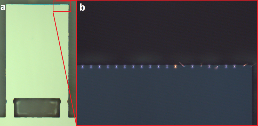
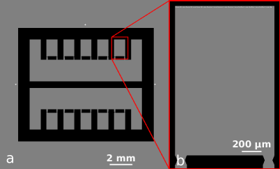
To define the device pattern, an anisotropic deep reactive ion etch (DRIE) using the Bosch process 5 was used. 700 Bosch cycles were run in an Oxford Instuments PlasmaLab System 100 to completely etch through the substrate to define the final shape of the device. This allowed us to locate NWs at the edge of the chip, allowing for them to be optically accessible. We also found that growing NWs in close proximity to the edge of a chip resulted in a slightly increased yield of vertical NWs compared to NWs patterned in the center if a chip.
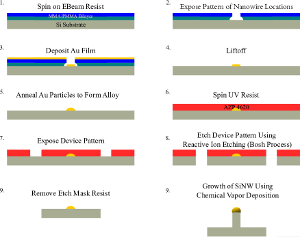
The mask (Figure S2) used for the DRIE process was a double layer AZP 4620 photoresist with a total thickness of approximately 21 m. The thickness of the resist allows it to withstand the long etch process, protecting the gold dots during the etch. The device pattern was defined using UV lithography in a Heidelberg MLA 150 Direct Write UV Lithography system and developed in AZ 400K for 4 min. The mask pattern is aligned to the three alignment marks (Figure S2) that were patterned during the EBL and Au evaporation steps. Defining the etch mask in this way allows us to align to our patterned gold dots with high accuracy, typically to within 1–2 m of the desired location.
After the DRIE, the etch mask was removed by sonicating in PG remover at 80 ∘C for 40 min. It was found on some samples that localized heating during the etch process led to hardbaking of the etch mask, causing microscopic photoresist contamination to remain even after removal of the mask. This remaining contamination was removed by immersing the sample in the SC-1 solution described above at 70 ∘C for 15 min to remove any remaining organic material. A diagram of the described fabrication process is presented in Figure S1.

Growth of the SiNWs was done in a FirstNano EasyTube 3000EXT Chemical Vapor Deposition (CVD) system using the vapor-liquid-solid (VLS) mechanism 6. Our growth process takes place at 550 ∘C and an absolute pressure of 4 Torr.
After the final SC-1 clean, we load our sample into the furnace tube of the CVD system heated to 100 ∘C overnight. This allows us dehydration bake the sample to remove any moisture that may have accumulated during transit to the CVD system.
The process furnace is ramped to 550 ∘C under a 1 SLM H2 flow. We found that growing at 550 ∘C provided a significantly higher yield of vertical NWs compared to higher temperatures 7. At temperatures lower than 550 ∘C, we observed a reduced yield of vertical NWs. We also observed that some of the catalyst particles failed to nucleate at lower temperatures, leading to fewer NWs growing overall.
During the temperature ramp, the pressure is kept at 4 Torr by a variable speed pump. Once the furnace temperature has stabilized, process gases are introduced to the system. A 20 SCCM flow of Hydrogen Chloride (HCl) and a 10 SCCM flow of Silane (SiH4) are introduced. These flow rates result in partial pressures of Torr, mTorr, mTorr. H2 acts as a carrier gas, and allows dangling bonds on the newly grown Si surface to be passivated by hydrogen termination. SiH4 acts as a precursor, providing the source of Si to be deposited via the Au catalyst particle. The presence of HCl has been shown to prevent breakup of the catalyst particle during growth and to suppress radial growth on the NW side walls by etching the side walls during growth. 8, 9. This allows us to grow NWs with clean side walls, and little to no taper. We observed that the prevention of sidewall growth contributes to achieving a high quality factor. To achieve a SiNW length of 23 m, we maintain the flow of process gases for a period of 3 h. Under these conditions NWs grow at a constant rate, allowing us to control their length by varying the growth time.
Once the growth process is complete, the flow of process gas is cut off and the furnace tube is allowed to cool under a H2 flow to 300 ∘C. The tube is then evacuated, filled with N2, and allowed to cool to room temperature over a period of roughly 1 h under a N2 flow.
2 Comparison of frequency determination methods
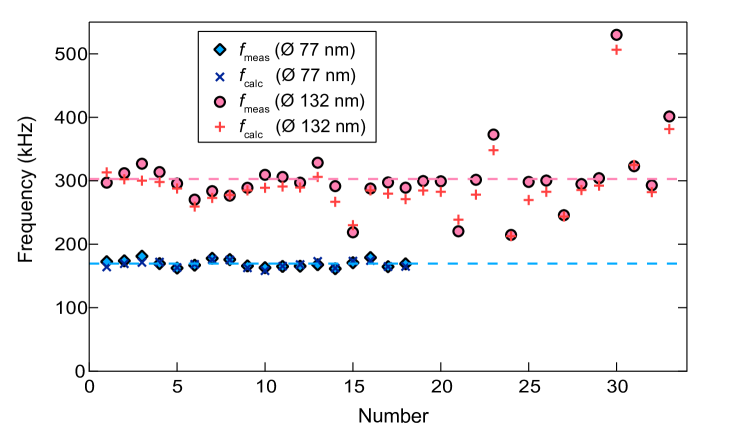
The mechanical dissipation of a flexural mode of the SiNWs is given by , where is the spring constant, the angular frequency, and the quality factor of the mode. The frequencies and quality factors for the two fundamental modes of each wire can be determined accurately by fitting the double-resonance lineshape, Eq. (4), to the power spectral density obtained by interferometry. However, determining by interferometry is much less straightforward. Instead, ’s were calculated by Eq. (1) using radius, , and length, , for each wire as measured by scanning electron microscopy. To confirm the accuracy of these dimension measurements and the validity of this determination, frequencies measured at room temperature by interferometry were compared to frequencies calculated using Eq. (2), which also depends on and . Full data are shown in Fig. S5 and Table S1. Taking to be the correct value, the average error in was 3.6% for the larger SiNWs and 1.2% for the smaller SiNWs. Because depends more strongly than on and , the error in may be slightly larger.
| Error | ||||
| (nm) | (kHz) | (kHz) | (%) | |
| Array 1 | 132 10 | 291 49 | 302 54 | 3.6 |
| Array 2 | 77 1 | 168 5 | 170 6 | 1.2 |
3 Displacement sensitivity and SiNW heating
A fiber-coupled distributed-feedback 1510 nm laser was used for the interferometer. A splitter sent 95% of the optical power to a monitor photodiode. The remaining 5% traveled through a three paddle polarization controller and then into the probe. The fiber end inside the probe was cleaved, which reflected about 3% light and served as our reference beam. The remaining light was focused by a Lightpath 355631 lens with a working distance of 280 m and a numerical aperture of 0.55. The light was detected with an InGaAs PIN photodiode and amplified with a FEMTO DHPCA-100 transimpedance amplifier. Fig 1b shows a schematic of the interferometer.
The equipartition theorem was used to determine SiNW temperature:
| (S1) |
where is the Boltzmann constant, represents a single flexural mode, is the spring constant of that mode, and is the time-averaged squared displacement of the mode. Since the lowest-frequency two modes are nearly degenerate and randomly oriented, the combined projection of both modes onto the optical axis was measured, given by: . Assuming , and using (S1), gives . However, for this equation, must be measured at the tip of the nanowire. Due to the m spot size, it is difficult to locate the tip accurately, and one is forced to average over some length of the NW. Instead, was measured at multiple laser powers, including at several very low powers. A line was fit to the lowest three values of . The temperature was assumed to be 4.2 K at zero laser power, and the values were scaled accordingly to produce Fig. S6b.
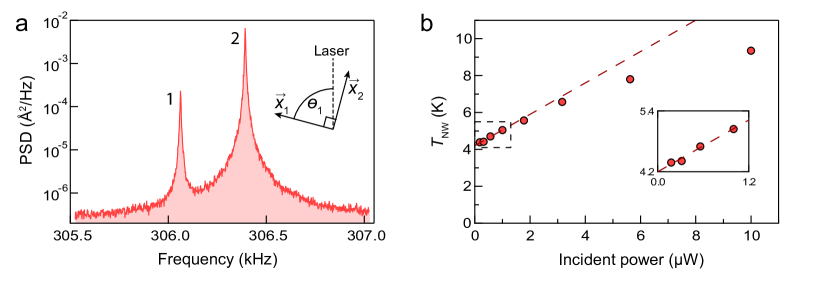
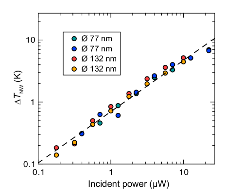
Heating and displacement sensitivity measurements were made on four SiNWs, two from each array, at 4.2 K. Heating was observed to be similar for all four SiNWs for a given incident power, as shown in Fig. S7, meaning that it was independent of nanowire diameter. Although this was not studied in detail, the thermal resistance at a given temperature is approximately inversely proportional to the cross-sectional area, suggesting that the absorbed power is roughly directly proportional to the cross-sectional area of the SiNW. We fit the heating data with a power law, , where P is the incident power, and A and B are the fit parameters. This relationship between incident power and SiNW heating was used to produce the heating axis in Fig. 3.
To extend measurements to lower temperatures but maintain displacement sensitivity around one could attempt to modify the optical interactions with the nanowire, or one could improve the optics electronics. As seen in Fig. 3, the shot noise is significantly lower than the total noise, which was dominated by noise from the transimpedance amplifier. One change that could substantially improve the displacement sensitivity at low incident powers would be switching from a PIN photodiode to an avalanche photodiode. Photocurrent gains of 10 or more are possible with InGaAs avalanche photodiodes, meaning that one could obtain the same signal strength with 10 times less incident power, and therefore much less heating.
References
- Kang and Musgrave 2002 Kang, J.; Musgrave, C. The mechanism of HF/H2O chemical etching of SiO2. J. Chem. Phys. 2002, 116, 275
- Bal et al. 2010 Bal, J.; Kundu, S.; Hazra, S. Hydrophobic to hydrophilic transition of HF-treated Si surface during Langmuir–Blodgett film deposition. Chem. Phys. Lett. 2010, 500, 90–95
- Pinardi et al. 2009 Pinardi, A. L.; Leake, S. J.; Felici, R.; Robinson, I. K. Formation of an Au-Si eutectic on a clean silicon surface. Phys. Rev. B 2009, 79, 045416
- Ressel et al. 2003 Ressel, B.; Prince, K. C.; Heun, S. Wetting of Si surfaces by Au–Si liquid alloys. J. Appl. Phys. 2003, 93, 3886
- Laermer and Schilp 1996 Laermer, F.; Schilp, A. Method of anisotropically etching silicon. U.S. Patent 5,501,893, 1996
- Wagner and Ellis 1964 Wagner, R. S.; Ellis, W. C. Vapor-Liquid-Solid Mechanism of Single Crystal Growth. Appl. Phys. Lett. 1964, 4, 89
- Schmid et al. 2008 Schmid, H.; Björk, M. T.; Knoch, J.; Riel, H.; Riess, W.; Rice, P.; Topuria, T. Patterned epitaxial vapor-liquid-solid growth of silicon nanowires on Si(111) using silane. J. Appl. Phys. 2008, 103, 024304
- Oehler et al. 2009 Oehler, F.; Gentile, P.; Baron, T.; Ferret, P. The effects of HCl on silicon nanowire growth: surface chlorination and existence of a ’diffusion-limited minimum diameter’. Nanotechnology 2009, 20, 475307
- Gentile et al. 2012 Gentile, P.; Solanki, A.; Pauc, N.; Oehler, F.; Salem, B.; Rosaz, G.; Baron, T.; Hertog, M. D.; Calvo, V. Effect of HCl on the doping and shape control of silicon nanowires. Nanotechnology 2012, 23, 215702