Unveiling multiferroic proximity effect in graphene
Abstract
We demonstrate that electronic and magnetic properties of graphene can be tuned via proximity of multiferroic substrate. Our first-principles calculations performed both with and without spin-orbit coupling clearly show that by contacting graphene with bismuth ferrite BiFeO3 (BFO) film, the spin-dependent electronic structure of graphene is strongly impacted both by the magnetic order and by electric polarization in the underlying BFO. Based on extracted Hamiltonian parameters obtained from the graphene band structure, we propose a concept of six-resistance device based on exploring multiferroic proximity effect giving rise to significant proximity electro- (PER), magneto- (PMR), and multiferroic (PMER) resistance effects. This finding paves a way towards multiferroic control of magnetic properties in two dimensional materials.
Spintronic devices possessing high speed and low-power consumption have opened new prospects for information technologies. As the spin generation, manipulation, and detection is the operating keystone of a spintronic device, realizing those three components simultaneously stands as a major challenge limiting applications 1, 2, 3, 4. In this context, developing a suitable spin transport channel which retains both long spin lifetime and diffusion length is highly desirable. Graphene stands as a potential spin channel material owing to its exceptional physical properties. Beside its high electron mobility and tunable-charge carrier concentration, graphene has demonstrated room temperature spin transport with long spin-diffusion lengths 5, 6, 7, 8, 9, 10, 11, 12, 13, 14, 15. Accordingly, graphene spintronics became a promising direction of innovation that attracted a growing attention in the scientific community 16, 17.
Much efforts have been devoted to induce magnetism in graphene via different means 18, 19, 20, 21, 22, 23, 24, 25, 26, 27, 28, 29, 30, 31, 32, 33, one of which is the exchange-proximity interaction with magnetic insulators 34, 35, 36. Theoretically, this effect was demonstrated using different materials such as ferromagnetic 37, 38, antiferromagnetic 39, topological 40, and multiferroic 41 insulators where exchange-splitting band gaps reaching up to 300 meV were demonstrated. Recently, a detailed study has shown the influence of different magnetic insulators on the magnetic proximity effect induced in graphene 42. On the other hand, experiments on YIG/Gr 34, 43, 35, 44, EuS/Gr 45, and BFO/Gr 46, 47 demonstrated proximity induced effect in graphene with substantial exchange field reaching T. However, combining both conditions of a high Curie temperature () magnetic insulator and a weak graphene doping stands as a major challenge which limits practical spintronic applications.
Multiferroics, co-exhibiting a magnetic and ferroelectric order, constitute an interesting class of magnetic insulators that bring about an additional parameter in play which is the electric polarization. On one hand, proximity induced magnetism was reported in graphene using multiferroic magnetic insulator 41, 48, 39 ignoring the influence of electric polarization. On the other hand, the ferroelectrically-driven manipulation of the carrier density in graphene was demonstrated 49. However, the ferroelectric control of magnetic proximity effect has not been addressed so far. In this letter, we report the multiferroic-induced proximity effect (MFPE) in graphene proposing the concept of controlling electronic and magnetic properties of graphene via multifferoic substrate. For this purpose, we considered bismuth ferrite BiFeO3 (BFO) whose room-temperature multiferroicity promotes it as a good candidate for applications 50, 51, 52, 53, 54. Our first-principles calculations demonstrate that by contacting graphene with BFO, the spin-dependent electronic structure of graphene is highly influenced not only by the magnetic order but also by the ferroelectric polarization in the underlying BFO. These findings propose additional degrees of control for proximity induced phenomena in graphene and perhaps in other two-dimensional materials.
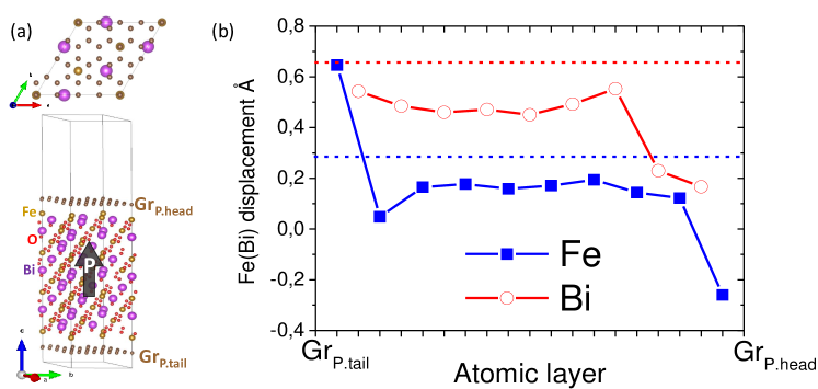
Our first-principles calculations are based on the projector-augmented wave (PAW) method 55 as implemented in the VASP package 56, 57, 58 using the generalized gradient approximation as parametrized by Perdew,Burke, and Ernzerhof 59, 60. A kinetic energy cutoff of 550 eV has been used for the plane-wave basis set and a -point mesh to sample the first Brillouin zone. The supercell comprises of nine (Bi-O3-Fe) trilayers of BFO () surface with Fe termination sandwiched between two graphene layers as shown in Figure 1 (a). We fixed the in plane lattice parameter to that of BFO where the lattice mismatch in this supercell configuration is about . This heterostructure provides the opportunity to compare simultaneously the properties of two different graphene layers relatively sensing opposite directions of the BFO polarization . Since maintaining the polarization is a critical issue in ferroelectric slabs, a thick BFO slab is used both to restore the electric polarization within the bulk layers and to assure that the two graphene layers do not interact. At both Gr/BFO interfaces, one Fe atom is placed at a hollow site whereas the other two atoms occupy top sites as shown in the top view of Figure 1 (a). Then, the atoms were allowed to relax in all directions until the forces became lower than meV/Å. As the GGA fails to describe the electronic structure of strongly correlated oxides, we have employed the GGA+U method to the Fe-d orbitals 61. We have optimized the value of using the bulk unit cell of BFO and found that eV yields eV band gap and /Fe magnetic moments which are in good agreement with experimental values 62, 63, 64.
BiFeO3 has a perovskite type cryctal structure and belongs to the polar space group . The spontaneous polarization along BFO (111) direction originates from the displacements of the Bi and Fe atoms from their centrosymmetric positions along the (111) direction 63, 52, 50. To examine of BFO after the formation of the Gr/BFO/Gr interfaces which accounts for both the ionic and charge relaxation, we show in Figure 1(b) the Fe and Bi -displacements from their centrosymmetric positions per atomic layer. It can be clearly seen that the two BFO/Gr interfaces have different values of atomic displacements whereas in the bulk layers the values are almost constant in good relevance to the bulk values (shown by dashed lines). This infers that , which arises from such non-centrosymmetric structure, is sustained in BFO and it is perpendicular to the interface and pointing from lower graphene layer, lying at the tail of and denoted hereafter by GrP.tail, towards the upper one lying at the head of denoted by GrP.head. A rough estimate of the -averaged polarization can be deduced from the values of the local polarization based on Born effective charges: ; where N is the number of atoms, is the displacement of the th atom from the centrosymmetric position, is the volume of the unit cell, and is the Born effective charge of the th ion. In our supercell a value of C/cm2 is estimated which reasonably compares to the calculated value in a bulk BFO unit cell C/cm2 50.
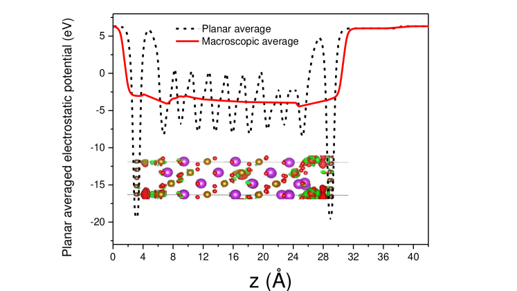
We discuss now the formation of Gr/BFO/Gr interface. The BFO(111) slab is Fe3+ terminated on both sides which makes the two surfaces polar with a nonzero net charge. From a macroscopic electrostatic point of view, this is equivalent to a slab having a polar surface charge on both surfaces and no charges inside the slab, where is the surface area per Fe atom. On the other hand, assuming a uniform polarization in the BFO slab whose direction is shown in Figure 1(a) yields surface polarization charges and on the head and tail surfaces, respectively. Therefore, the whole BFO slab is equivalent to a slab with total bound charge on the head surface and on the tail surface. This dissimilarity in the BFO surface charges leads to the formation of two significantly different interfaces with graphene giving rise to two adsorption distances Å compared to Å. In fact, graphene sheets adsorbed on both sides of the slab accumulate negative charges trying, ideally, to screen the positive bound charges on the BFO surfaces. This produces a strong electrostatic interaction between graphene and the BFO surfaces in particular at the head interface where the bound charges are quantitatively larger as shown in Figure 2. Consequently, (i) the relaxes closer to the BFO surface compared to and (ii) strong relaxations are induced at the head BFO surface revelaed by the smaller polar displacements at the outermost layers, as shown in Figure 1(b), thus, reducing the effective polarization at this surface.
To get more insights on the interaction at the Gr/BFO/Gr interfaces, the inset of Figure 2 shows the induced charge distribution upon the formation of the interfaces. Negative charges, represented by red regions, are accumulated at both Gr/BFO interfaces in accord with the description we provided in the previous paragraph. However, the charges at the GrP.head are obviously larger than at the GrP.tail. This is a direct implication of the stronger electrostatic interaction at the head interface which is responsible for the shorter interfacial distance.
| GrP.head | -48.6 | 55 | 26 | 104 | 75 | -0.85 | 4 | 2.66 | 2.3 | 8.7 |
| 2.66 | 2.28 | |||||||||
| 2.61 | 2.32 | |||||||||
| GrP.tail | -34.04 | 6 | 1.5 | -35 | -40 | -0.47 | 5 | 2.42 | 2.5 | 7.5 |
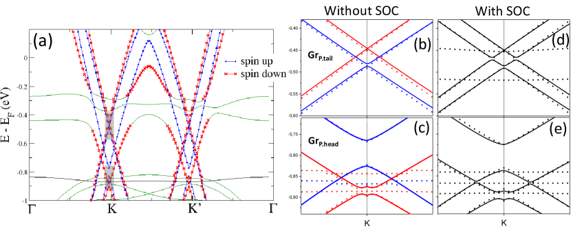
We discuss now the induced multiferroic-proximity effect in graphene by BFO. As we have demonstrated that the two graphene sheets exhibit different interaction strengths with the underlying BFO surface, the corresponding proximity effect is expected to differ. The calculated band structure for Gr/BFO/Gr supercell, displayed in Figure 3 (a), reveals two distinct graphene band dispersions highlighted by blue and red corresponding to spin up and spin down, respectively. However, both graphene sheets are negatively doped which is expected due to accumulated negative charges on graphene side in response to the positive bound charges at both BFO surfaces. Following its weaker interaction with BFO, the Dirac cone corresponding to GrP.tail, shown in Figure 3(b) lies in the bulk gap of BFO closer to the Fermi level. On the other hand, the stronger interaction at GrP.head/BFO interface results in a larger doping of the Dirac point, as seen in Figure 3 (c). The proximity of the insulating BFO induces modifications in the linear dispersion of the graphene band structure opening a band gap at the Dirac point. This degeneracy lifting at the Dirac point is spin dependent owing to the interaction with the magnetic BFO substrate. Interestingly, the spin-dependent band gaps and exchange splittings are influenced by the interaction strength at the BFO interface. Spin dependent band-gaps are found to be () meV for spin up (spin down) in GrP.head, whereas smaller values of () meV are reported for GrP.tail. Moreover, the spin splittings for GrP.head are found to be () meV for electrons (holes), respectively, compared to () meV for GrP.tail. Figure 3 (d,e) show the evolution of the graphene band structure upon adding spin-orbit coupling to the calculations. The main impact of the spin-orbit interaction is inducing an additional band opening denoted by at the spin up/spin down band crossings. We find corresponding values of and meV for GrP.head and GrP.tail, respectively.
The parameters obtained from the band structure are summarized in Table 1 for both GrP.head and GrP.tail. and represent the energy band gap and the spin dependent band gaps, respectively. The spin splitting of the electron and hole bands are denoted as and . indicates how large the Dirac point doping is with respect to Fermi energy and is the spin-orbit coupling induced band opening. The negative value of indicates a spin resolved band overlap while spin splittings are defined by spin-dependent energy differences at Dirac point with negative value indicating that spin-up bands are lower in energy than that of spin-down bands. Due to the stronger interaction at the head interface compared to the tail, the proximity-induced gaps and splittings are larger in Grhead. However, the spin orbit coupling induced gap is rather smaller. We should note here that our calculated values are different from those obtained in Ref 39 due basically to the difference in the -mesh size. As the band structure of graphene is highly sensitive to the k-mesh, we have used a dense -mesh in our calculations.
The following tight-binding Hamiltonian describes the graphene’s linear dispersion relation in proximity of a magnetic insulator:
| (1) |
where is the anisotropic hopping connecting unit cells to their nearest neighbors cells . creates an electron of type () corresponding to A and B sites, respectively, on the unit cell with spin () for spin up and spin down electrons, respectively. where and is the strength of the exchange spin-splitting of the electron and hole bands at the Dirac cone, respectively. is a unit vector that points in the direction of the magnetization and is the vector of Pauli matrices, so that . is the Dirac position with respect to the Fermi level and is the averaged staggered sublattice potential. The Rashba spin orbit coupling term is written as 65, 66,
| (2) |
where is the Rashba spin orbit coupling strength and the vector connects the two nearest neighbors.
To obtain the hopping values, the tight binding bands where fitted in good accordance to the DFT bands as shown by solid lines in Figures 3(b-e). In the case of GrP.head, it was necessary to include direction dependent hopping parameters into the model. The values of the hopping parameters used for both GrP.head and GrP.tail are listed in Table 1.
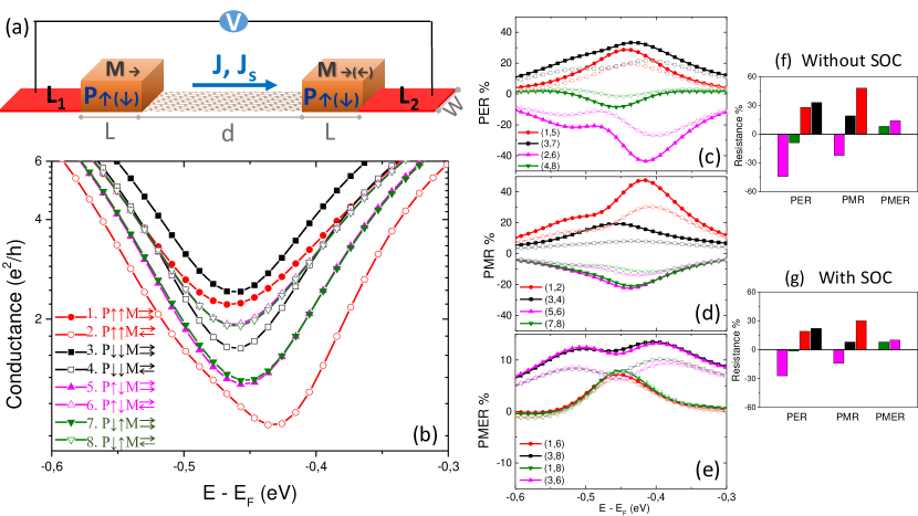
Based on the Hamiltonian parameters extracted from the graphene band structure, we employed the tight-binding approach with scattering matrix formalism conveniently implemented within the KWANT package in order to calculate conductances and proximity resistances 67. The system modeled is shown in 4(a) and comprises two identical proximity induced multiferroic regions of width nm and length nm, separated by a distance nm of nonmagnetic region of graphene sheet with armchair edges. Both magnetic graphene regions are connected to the leads and and modeled using the Hamiltonian parameters. All the relative magnetization and polarization configurations are considered in this model device. The conductance in the linear response regime can be obtained according to:
| (3) |
where indicates spin-dependent transmission probability with () and () being, respectively, the relative polarization and magnetization configurations in the multiferroic regions. is the Fermi-Dirac distribution in which and indicate electrochemical potential and temperature, respectively. It is important to mention that the temperature smearing has been taken into account using the room temperature since the Curie termperature of BFO is well above it. In order to show the impact of polarization on transport calculations, we choose to adjust the doping energy for the GrP.head to be the same as for GrP.tail bands. The conductance curves shown in Figure 4(b), which are explicitly described in the legend and indexed by numbers, reveal six different resistance states two of which are degenerate; those are ( and ) and ( and ). The conductance for a given energy should be seen as if one could gate the whole device to bring the region of interest, in the vicinity of the Dire cone splittings, to the Fermi level. We observe that the conductance curves are splitted the most in the energy range affected by proximity effect which is around eV. Since the gaps and exchange splittings are much larger for GrP.head compared to GrP.tail, a difference in the energies and conductance values between the corresponding conductance states is observed.
The different combinations of these conductance states give rise to three types of proximity resistances: proximity electroresistance (PER), proximity magnetoresistance (PMR), and proximity multiferroic resistance (PMER). We introduce the generalized formulas of these three types of proximity resistances as follows:
| (4) |
| (5) |
| (6) |
Based on this formalism, sixteen different conductance states are expected. However, due to symmetry in our considered model device we obtain and and, consequently, we end up with six conductance states .
The calculated PER, PMR, and PMER are plotted in Figure 4(c),(d), and (e), respectively, in which the indices of the two conductance states used to obtain each proximity resistance curve are designated. Closed (open) symbol lines correspond to the calculations without (with) including SOC. Owing to the two degenerate conductance states, we obtain one (two) degenerate PMR (PMER) curves, correspondingly. The PER values range between and , PMR has values from to , whereas PMER ranges between and . We should note that including SOC doesn’t change our results qualitatively but rather decreases the values of the conductances and consequently the values of the different types of proximity resistances as shown in Figure 4(f,g). This is basically due to the mixing of the spin channels imposed by the spin-orbit interaction. Our findings lead to a concept of multi-resistance device and pave a way towards multiferroic control of magnetic properties in two-dimensional materials. Interestingly, recent experiments have demonstrated the electric control of magnetic proximity effect at the graphene/BFO interface 68 which further enhances the possibility of realizing our proposed concept device.
In conclusion, we have demonstrated that the magnetic proximity effect in graphene can be tuned by the electric polarization existing in the multiferroic substrate. The presence of electric polarization together with the polar surface charges lead to different interaction strength at the Gr/BFO interface depending on the relative direction of the electric polarization. Consequently, the spin-dependent band gaps and exchange splittings are impacted. Those findings suggest tuning the magnetic proximity effect in graphene through altering the direction or even the magnitude of the electric polarization. Such approach is accessible in multiferroic oxides where the interplay between electric and magnetic order offers the possibility of tuning the magnetization and polarization by applying electric or magnetic fields, respectively.
We thank J. Fabian, K. Zollner and S. Roche for fruitful discussions. This project has received funding from the European Union’s Horizon 2020 research and innovation programme under grant agreements No. 696656 and 785219 (Graphene Flagship).
References
- Chappert et al. 2007 Chappert, C.; Fert, A.; Dau, F. N. The emergence of spin electronics in data storage. Nature Materials 2007, 6, 813–823
- Zutić et al. 2004 Zutić, I. .; Fabian, J.; Sarma, S. D. Spintronics: Fundamentals and applications. Reviews of Modern Physics 2004, 76, 323
- Lou et al. 2007 Lou, X.; Adelmann, C.; Crooker, S. A.; Garlid, E. S.; Zhang, J.; Reddy, K. S. M.; Flexner, S. D.; Palmstrøm, C. J.; Crowell, P. A. Electrical detection of spin transport in lateral ferromagnet–semiconductor devices. Nature Physics 2007, 3, 197–202
- Dash et al. 2009 Dash, S. P.; Sharma, S.; Patel, R. S.; Jong, M. P. D.; Jansen, R. Electrical creation of spin polarization in silicon at room temperature. Nature 2009, 462, 491–494
- Geim and Novoselov 2007 Geim, A. K.; Novoselov, K. S. The rise of graphene. Nature Materials 2007, 6, 183–191
- Neto et al. 2009 Neto, A. H. C.; Guinea, F.; Peres, N. M. R.; Novoselov, K. S.; Geim, A. K. The electronic properties of graphene. Reviews of Modern Physics 2009, 81, 109
- Tombros et al. 2007 Tombros, N.; Jozsa, C.; Popinciuc, M.; Jonkman, H. T.; van Wees, B. J. Electronic spin transport and spin precession in single graphene layers at room temperature. Nature 2007, 448, 571–574
- Popinciuc et al. 2009 Popinciuc, M.; Józsa, C.; Zomer, P. J.; Tombros, N.; Veligura, A.; Jonkman, H. T.; van Wees, B. J. Electronic spin transport in graphene field-effect transistors. Physical Review B 2009, 80, 214427
- Dlubak et al. 2010 Dlubak, B.; Seneor, P.; Anane, A.; Barraud, C.; Deranlot, C.; Deneuve, D.; Servet, B.; Mattana, R.; Petroff, F.; Fert, A. Are Al2O3 and MgO tunnel barriers suitable for spin injection in graphene? Applied Physics Letters 2010, 97, 092505
- Han and Kawakami 2011 Han, W.; Kawakami, R. K. Spin Relaxation in Single-Layer and Bilayer Graphene. Physical Review Letters 2011, 107, 047207
- Yang et al. 2011 Yang, T.-Y.; Balakrishnan, J.; Volmer, F.; Avsar, A.; Jaiswal, M.; Samm, J.; Ali, S. R.; Pachoud, A.; Zeng, M.; Popinciuc, M.; Güntherodt, G.; Beschoten, B.; Özyilmaz, B. Observation of Long Spin-Relaxation Times in Bilayer Graphene at Room Temperature. Physical Review Letters 2011, 107, 047206
- Maassen et al. 2012 Maassen, T.; van den Berg, J. J.; IJbema, N.; Fromm, F.; Seyller, T.; Yakimova, R.; van Wees, B. J. Long Spin Relaxation Times in Wafer Scale Epitaxial Graphene on SiC(0001). Nano Letters 2012, 12, 1498–1502
- Dlubak et al. 2012 Dlubak, B.; Martin, M.-B.; Deranlot, C.; Servet, B.; Xavier, S.; Mattana, R.; Sprinkle, M.; Berger, C.; Heer, W. A. D.; Petroff, F.; Anane, A.; Seneor, P.; Fert, A. Highly efficient spin transport in epitaxial graphene on SiC. Nature Physics 2012, 8, 557–561
- Cummings and Roche 2016 Cummings, A. W.; Roche, S. Effects of Dephasing on Spin Lifetime in Ballistic Spin-Orbit Materials. Physical Review Letters 2016, 116, 086602
- Tuan et al. 2016 Tuan, D. V.; Ortmann, F.; Cummings, A. W.; Soriano, D.; Roche, S. Spin dynamics and relaxation in graphene dictated by electron-hole puddles. Scientific Reports 2016, 6, 21046
- Roche et al. 2015 Roche, S. et al. Graphene spintronics: the European Flagship perspective. 2D Materials 2015, 2, 030202
- Han et al. 2014 Han, W.; Kawakami, R. K.; Gmitra, M.; Fabian, J. Graphene spintronics. Nature Nanotechnology 2014, 9, 794–807
- Yazyev and Helm 2007 Yazyev, O. V.; Helm, L. Defect-induced magnetism in graphene. Physical Review B 2007, 75, 125408
- Yazyev 2008 Yazyev, O. V. Magnetism in Disordered Graphene and Irradiated Graphite. Physical Review Letters 2008, 101, 037203
- Yazyev 2010 Yazyev, O. V. Emergence of magnetism in graphene materials and nanostructures. Reports on Progress in Physics 2010, 73, 056501
- Son et al. 2006 Son, Y.-W.; Cohen, M. L.; Louie, S. G. Half-metallic graphene nanoribbons. Nature 2006, 444, 347–349
- Kim and Kim 2008 Kim, W. Y.; Kim, K. S. Prediction of very large values of magnetoresistance in a graphene nanoribbon device. Nature Nanotechnology 2008, 3, 408–412
- Bai et al. 2010 Bai, J.; Zhong, X.; Jiang, S.; Huang, Y.; Duan, X. Graphene nanomesh. Nature Nanotechnology 2010, 5, 190–194
- Yang et al. 2011 Yang, H.-X.; Chshiev, M.; Boukhvalov, D. W.; Waintal, X.; Roche, S. Inducing and optimizing magnetism in graphene nanomeshes. Physical Review B 2011, 84, 214404
- Trolle et al. 2013 Trolle, M. L.; Møller, U. S.; Pedersen, T. G. Large and stable band gaps in spin-polarized graphene antidot lattices. Physical Review B 2013, 88, 195418
- Soriano et al. 2011 Soriano, D.; Leconte, N.; Ordejón, P.; Charlier, J.-C.; Palacios, J.-J.; Roche, S. Magnetoresistance and Magnetic Ordering Fingerprints in Hydrogenated Graphene. Physical Review Letters 2011, 107, 016602
- McCreary et al. 2012 McCreary, K. M.; Swartz, A. G.; Han, W.; Fabian, J.; Kawakami, R. K. Magnetic Moment Formation in Graphene Detected by Scattering of Pure Spin Currents. Physical Review Letters 2012, 109, 186604
- Chan et al. 2008 Chan, K. T.; Neaton, J. B.; Cohen, M. L. First-principles study of metal adatom adsorption on graphene. Physical Review B 2008, 77, 235430
- Ding et al. 2011 Ding, J.; Qiao, Z.; Feng, W.; Yao, Y.; Niu, Q. Engineering quantum anomalous/valley Hall states in graphene via metal-atom adsorption: An ab-initio study. Physical Review B 2011, 84, 195444
- Zhang et al. 2012 Zhang, H.; Lazo, C.; Blügel, S.; Heinze, S.; Mokrousov, Y. Electrically Tunable Quantum Anomalous Hall Effect in Graphene Decorated by 5d Transition-Metal Adatoms. Physical Review Letters 2012, 108, 056802
- Jiang et al. 2012 Jiang, H.; Qiao, Z.; Liu, H.; Shi, J.; Niu, Q. Stabilizing Topological Phases in Graphene via Random Adsorption. Physical Review Letters 2012, 109, 116803
- Kim and Kim 2010 Kim, W. Y.; Kim, K. S. Tuning Molecular Orbitals in Molecular Electronics and Spintronics. Accounts of Chemical Research 2010, 43, 111–120
- Yang et al. 2011 Yang, J. W.; Lee, G.; Kim, J. S.; Kim, K. S. Gap Opening of Graphene by Dual FeCl3-Acceptor and K-Donor Doping. Journal of Physical Chemistry Letters 2011, 2, 2577–2581
- Wang et al. 2015 Wang, Z.; Tang, C.; Sachs, R.; Barlas, Y.; Sh, J. Proximity-Induced Ferromagnetism in Graphene Revealed by the Anomalous Hall Effect. Physical Review Letters 2015, 114, 016603
- Leutenantsmeyer et al. 2017 Leutenantsmeyer, J. C.; Kaverzin, A. A.; Wojtaszek, M.; van Wees, B. J. Proximity induced room temperature ferromagnetism in graphene probed with spin currents. 2D Materials 2017, 4, 014001
- Singh et al. 2017 Singh, S.; Katoch, J.; Zhu, T.; Meng, K.-Y.; Liu, T.; Brangham, J. T.; Yang, F.; Flatté, M. E.; Kawakami, R. K. Strong Modulation of Spin Currents in Bilayer Graphene by Static and Fluctuating Proximity Exchange Fields. Physical Review Letters 2017, 118, 187201
- Yang et al. 2013 Yang, H. X.; Hallal, A.; Terrade, D.; Waintal, X.; Roche, S.; Chshiev, M. Proximity Effects Induced in Graphene by Magnetic Insulators: First-Principles Calculations on Spin Filtering and Exchange-Splitting Gaps. Physical Review Letters 2013, 110, 046603
- Sakai et al. 2016 Sakai, S.; Majumdar, S.; Popov, Z. I.; Avramov, P. V.; Entani, S.; Hasegawa, Y.; Yamada, Y.; Huhtinen, H.; Naramoto, H.; Sorokin, P. B.; Yamauchi, Y. Proximity-Induced Spin Polarization of Graphene in Contact with Half-Metallic Manganite. ACS Nano 2016, 10, 7532–7541
- Qiao et al. 2014 Qiao, Z.; Ren, W.; Chen, H.; Bellaiche, L.; Zhang, Z.; MacDonald, A.; Niu, Q. Quantum Anomalous Hall Effect in Graphene Proximity Coupled to an Antiferromagnetic Insulator. Physical Review Letters 2014, 112, 116404
- Vobornik et al. 2011 Vobornik, I.; Manju, U.; Fujii, J.; Borgatti, F.; Torelli, P.; Krizmancic, D.; Hor, Y. S.; Cava, R. J.; Panaccione, G. Magnetic Proximity Effect as a Pathway to Spintronic Applications of Topological Insulators. NanoLetters 2011, 11, 4079–4082
- Zanolli 2016 Zanolli, Z. Graphene-multiferroic interfaces for spintronics applications. Scientific Reports 2016, 6, 31346
- Hallal et al. 2017 Hallal, A.; Ibrahim, F.; Yang, H.; Roche, S.; Chshiev, M. Tailoring magnetic insulator proximity effects in graphene: first-principles calculations. 2D Materials 2017, 4, 025074
- Mendes et al. 2015 Mendes, J. B. S.; Alves Santos, O.; Meireles, L. M.; Lacerda, R. G.; Vilela-Leão, L. H.; Machado, F. L. A.; Rodríguez-Suárez, R. L.; Azevedo, A.; Rezende, S. M. Spin-Current to Charge-Current Conversion and Magnetoresistance in a Hybrid Structure of Graphene and Yttrium Iron Garnet. Physical Review Letters 2015, 115, 226601
- Evelt et al. 2017 Evelt, M.; Ochoa, H.; Dzyapko, O.; Demidov, V. E.; Yurgens, A.; Sun, J.; Tserkovnyak, Y.; Bessonov, V.; Rinkevich, A. B.; Demokritov, S. O. Chiral charge pumping in graphene deposited on a magnetic insulator. Physical Review B 2017, 95, 024408
- Wei et al. 2016 Wei, P.; Lee, S.; Lemaitre, F.; Pinel, L.; Cutaia, D.; Cha, W.; Katmis, F.; Zhu, Y.; Heiman, D.; Hone, J.; Moodera, J. S.; Chen, C.-T. Strong interfacial exchange field in the graphene/EuS heterostructure. Nature Materials 2016, 15, 711–716
- Wu et al. 2017 Wu, Y.-F. et al. Magnetic proximity effect in graphene coupled to a BiFeO3 nanoplate. Physical Review B 2017, 95, 195426
- Song et al. 2018 Song, H.-D.; Wu, Y.-F.; Yang, X.; Ren, Z.; Ke, X.; Kurttepeli, M.; Tendeloo, G. V.; Liu, D.; Wu, H.-C.; Yan, B.; Wu, X.; Duan, C.-G.; Han, G.; Liao, Z.-M.; Yu, D. Asymmetric Modulation on Exchange Field in a Graphene/BiFeO3 Heterostructure by External Magnetic Field. Nano Letters 2018, 18, 2435–2441
- Zanolli et al. 2018 Zanolli, Z.; Niu, C.; Bihlmayer, G.; Mokrousov, Y.; Mavropoulos, P.; Verstraete, M. J.; Blügel, S. Hybrid quantum anomalous Hall effect at graphene-oxide interfaces. Physical Review B 2018, 98, 155404
- Baeumer et al. 2015 Baeumer, C.; Saldana-Greco, D.; Martirez, J. M. P.; Rappe, A. M.; Shim, M.; Martin, L. W. Ferroelectrically driven spatial carrier density modulation in graphene. Nature Communication 2015, 6, 6371
- Neaton et al. 2005 Neaton, J. B.; Ederer, C.; Waghmare, U. V.; Spaldin, N. A.; Rabe, K. M. First-principles study of spontaneous polarization in multiferroic BiFeO3. Physical Review B 2005, 71, 014113
- Ravindran et al. 2006 Ravindran, P.; Vidya, R.; Kjekshus, A.; Fjellvåg, H.; Eriksson, O. Theoretical investigation of magnetoelectric behavior in BiFeO3. Physical Review B 2006, 74, 224412
- Wang et al. 2003 Wang, J.; Neaton, J. B.; Zheng, H.; Nagarajan, V.; Ogale, S. B.; Liu, B.; Viehland, D.; Vaithyanathan, V.; Schlom, D. G.; Waghmare, U. V.; Spaldin, N. A.; Rabe, K. M.; Wuttig, M.; Ramesh, R. Epitaxial BiFeO3 Multiferroic Thin Film Heterostructures. Science 2003, 299, 1719–1722
- Zavaliche et al. 2006 Zavaliche, F.; Yang, S. Y.; Zhao, T.; Chu, Y. H.; Cruz, M. P.; Eom, C. B.; Ramesh, R. Multiferroic BiFeO3 films: domain structure and polarization dynamics. Phase Transitions 2006, 79, 991–1017
- Béa et al. 2009 Béa, H. et al. Evidence for Room-Temperature Multiferroicity in a Compound with a Giant Axial Ratio. Physical Review Letters 2009, 102, 217603
- Blöchl 1994 Blöchl, P. E. Projector augmented-wave method. Physical Review B 1994, 50, 17953–17979
- Kresse and Hafner 1993 Kresse, G.; Hafner, J. Ab initio molecular dynamics for liquid metals. Physical Review B 1993, 47, 558–561
- Kresse and Furthmüller 1996 Kresse, G.; Furthmüller, J. Efficient iterative schemes for ab initio total-energy calculations using a plane-wave basis set. Physical Review B 1996, 54, 11169–11186
- Kresse and Furthmüller 1996 Kresse, G.; Furthmüller, J. Efficiency of ab-initio total energy calculations for metals and semiconductors using a plane-wave basis set. Computational Materials Science 1996, 6, 15–50
- P.Perdew et al. 1996 P.Perdew, J.; Burke, K.; Ernzerhof, M. Generalized Gradient Approximation Made Simple. Physical Review Letters 1996, 77, 3865–3868
- Kresse and Joubert 1999 Kresse, G.; Joubert, D. From ultrasoft pseudopotentials to the projector augmented-wave method. Physical Review B 1999, 59, 1758–1775
- Liechtenstein et al. 1995 Liechtenstein, A. I.; Anisimov, V. I.; Zaane, J. Density-functional theory and strong interactions: Orbital ordering in Mott-Hubbard insulators. Physical Review B 1995, 52, 5467R
- Sosnowska et al. 2002 Sosnowska, I.; Schäfer, W.; Kockelmann, W.; Andersen, K.; Troyanchuk, I. Crystal structure and spiral magnetic ordering of BiFeO3 doped with manganese. Applied Physics A 2002, 74, s1040–s1042
- Kubel and Schmid 1990 Kubel, F.; Schmid, H. Structure of a ferroelectric and ferroelastic monodomain crystal of the perovskite BiFeO3. Acta Crystallographica Section B 1990, B46, 698–702
- Ihlefeld et al. 2008 Ihlefeld, J. F.; Podraza, N. J.; Liu, Z. K.; Rai, R. C.; Xu, X.; Heeg, T.; Chen, Y. B.; Li, J.; Collins, R. W.; Musfeldt, J. L.; Pan, X. Q.; Schubert, J.; Ramesh, R.; Schlom, D. G. Optical band gap of BiFeO3 grown by molecular-beam epitaxy. Applied Physics Letters 2008, 92, 142908
- Kane and Mele 2005 Kane, C. L.; Mele, E. J. Quantum Spin Hall Effect in Graphene. Physical Review Letters 2005, 95, 226801
- Tse et al. 2011 Tse, W.-K.; Qiao, Z.; Yao, Y.; MacDonald, A. H.; Niu, Q. Quantum anomalous Hall effect in single-layer and bilayer graphene. Physical Review B 2011, 83, 155447
- Groth et al. 2014 Groth, C. W.; Wimmer, M.; Akhmerov, A. R.; Waintal, X. Kwant: a software package for quantum transport. New Journal of Physics 2014, 16, 063065
- Song et al. 2018 Song, H.-D.; Zhu, P.-F.; Yang, X.; Qin, M.; Ren, Z.; Duan, C.-G.; Han, G.; Liao, Z.-M.; Yu, D. Electrical control of magnetic proximity effect in a graphene/multiferroic heterostructure. Applied Physics Letters 2018, 113, 183101