Resonant and Bound States of Charged Defects in Two-Dimensional Semiconductors
Abstract
A detailed understanding of charged defects in two-dimensional semiconductors is needed for the development of ultrathin electronic devices. Here, we study negatively charged acceptor impurities in monolayer WS2 using a combination of scanning tunnelling spectroscopy and large-scale atomistic electronic structure calculations. We observe several localized defect states of hydrogenic wave function character in the vicinity of the valence band edge. Some of these defect states are bound, while others are resonant. The resonant states result from the multi-valley valence band structure of WS2, whereby localized states originating from the secondary valence band maximum at hybridize with continuum states from the primary valence band maximum at K/K′. Resonant states have important consequences for electron transport as they can trap mobile carriers for several tens of picoseconds.
Impurity doping is the prime technology to control the electrical conductivity of semiconductors over several orders of magnitude [1, 2]. Dopants introduce additional charge carriers that bind to the impurity and can be excited into the delocalized conduction or valence band states. Through this ionization process, the density of mobile charge carriers in the material is increased. However, the Coulomb potential induced by the positively charged donor or negatively charged acceptor scatters mobile charge carriers and thereby reduces carrier mobility.
Importantly, the Coulomb potential of charged impurities is screened by the dielectric response of the host semiconductor. The resulting perturbation leads to the formation of localized states composed of Bloch states near the band edges [3]. For bulk semiconductors, such as silicon or gallium arsenide, these defect states have hydrogenic wavefunctions [4, 5, 6, 7]. Because of the large dielectric constants and small effective masses of traditional bulk semiconductors, the wavefunctions extend over several nanometers and the corresponding binding energies are of the order of a few tenths of an electronvolt [8].
Many semiconductors exhibit multiple conduction or valence band valleys, i.e., their band structure features multiple extrema in the vicinity of the band gap. Such an electronic structure can result in the formation of resonant impurity states [9]. These states occur when a localized defect level originating from a secondary band extremum lies in the energy range of the continuum states of the primary band extremum [7]. The hybridization with the continuum states leads to an energy shift and a broadening of the localized level into a resonance. Such resonant defect states play an important role in transport properties [10, 11] because a mobile charge carrier can be temporarily trapped by the impurity, which reduces the carrier mobility [3].
Two-dimensional (2D) semiconductors, such as monolayer transition-metal dichalcogenides (TMDs), have been intensely studied over the last decade as promising candidates for nano-electronic components, optoelectronic devices, and quantum information applications [12, 13]. Understanding the properties of charged defects in these materials is a crucial step toward developing a viable route for impurity doping analogous to traditional (3D) semiconductors. A key difference between 2D and 3D semiconductors is their dielectric response to a charged perturbation. Specifically, the screened potential due to a point charge in 2D is not well-described by the bare Coulomb potential divided by a dielectric constant as in bulk semiconductors. Instead, in 2D semiconductors the dielectric response is relatively weak and highly anisotropic, which gives rise to strongly bound excitons that dominate their optical response [14, 15]. Unconventional screening of charged defects in monolayer TMDs with multi-valley band structure and large spin-orbit effects can also give rise to bound defect states with unusual properties, e.g., the prediction that the most strongly bound acceptor state switches from being of K/K′-valley character to -valley character at a critical value of the defect charge [16].
In this Letter, we study the electronic properties of charged impurities in monolayer WS2 on a graphene/SiC substrate using scanning tunneling microscopy / spectroscopy (STM/STS) and atomistic quantum-mechanical calculations. Using STS, we find that negatively charged impurities give rise to strong upwards band bending and a series of localized defect states in the vicinity of the valence band edge with - and -like character. Our calculations suggest that the -like states are bound defect states originating from either the K/K′ or valleys, while the -like states are resonant defect states which result from the hybridization of localized states from the valley with continuum states from the K/K′ valleys. Finally, we discuss the relevance of these findings for transport devices.
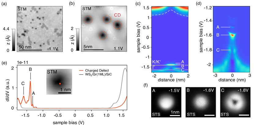
STM/STS measurements were performed under ultrahigh vacuum ( mbar) at low temperature (6 K). \ceWS2 samples were grown ex situ by chemical vapor deposition (CVD) on epitaxial graphene on silicon carbide substrates [17] and subsequent annealing in vacuum at 200∘C. A representative overview image of the surface is shown in Fig. 1(a). In our samples, we find various point defects, including oxygen-in-sulfur substitutions (OS), molybdenum-in-tungsten substitutions (MoW), and charged defects [see Fig. 1(b)], which we refer to as “CDs” and have identified in the figure with red dashed circles. [18] They are among the most abundant point defects in our samples but their density varies considerably between different CVD preparations. Similar STM contrast has been observed in CVD-grown MoS2 [19], MOCVD- and MBE-grown WSe2 [20, 21], MBE-grown MoSe2 [21] and natural bulk MoS2(0001) [22]. Some of these reports suggest that the observed defect might be charged [22, 21, 18] but their chemical origin remains unclear.
Non-contact atomic force microscopic (nc-AFM) imaging with a carbon monoxide (CO) functionalized tip [23] indicates that the charged defect is a chalcogen substitution [18]. The chemical origin of the CDs is yet unknown. Possible candidates include a CH or N substitution at the S site [18]. These substitutions introduce unoccupied defect states close the valence band edge of WS2. When the TMD is placed on the metallic graphene/SiC substrate, the Fermi level is pinned in the upper half of the WS2 band gap and the unoccupied defect states become filled due to charge transfer from the graphene [24]. As the hybridization between the WS2 states and the substrate is weak [25], the impurity charge is an integer multiple of the electron charge.
In constant-current STM imaging, CDs are observed as large depressions at positive sample bias and protrusions at negative sample bias. This is an electronic effect: a negative charge located at the CD site results in local upwards band bending. As shown in the spectra taken across a CD in Fig. 1(c), electrons are pushed to higher energies in the vicinity of the defect, leading to a position-dependent onset of the conduction band minimum (CBM), indicated with a white dashed line. The valence band of WS2 exhibits two primary maxima at the K and K′ points of the Brillouin zone and a secondary maximum at the point [see Fig. 2(a)]. The energies of these band extrema measured far away from the defect are indicated by white dotted lines in Fig. 1(c). It should be noted that states originating from the K/K′ point give only a weak STS signal. This is due to two factors: their relatively small effective mass results in a small local density of states (LDOS) and their large crystal momentum leads to a small tunnelling matrix element [26]. In contrast, the combination of a larger effective mass and a smaller crystal momentum at results in a stronger STS signal.
While there are no observed defect states near the CBM, several defect resonances are observed at negative bias in the vicinity of the valence band edge [see Figs. 1(c,d)]. In Fig. 1(e), we have labeled the three dominant resonances as “A”, “B”, and “C”, respectively. In addition, there are four very faint resonances observed just above state A [see the Supplementary Materials (SM) [27]]. We find that the localized defect states A and B lie on average 175 mV and 95 mV, respectively, above the onset of the K/K′ valence band edge (see Table 1), indicating that they are bound states. Resonance C lies mV below the K/K′ valence band edge, but mV above the onset of the valence band edge, suggesting that it is a resonant state, i.e., a localized state resonant with the continuum states from the K/K′ valleys.
| Experiment | Theory | |||
|---|---|---|---|---|
| K | K | |||
| A/meV | ||||
| B/meV | ||||
| C/meV | ||||
Spatially resolved maps of the states A, B, and C are shown in Fig. 1(f). States A and B have a spherical shape reminiscent of an -type orbital, whereas state C has three lobes and a node at its center, indicative of a trigonally warped -type orbital [16]. With a lateral dimension of about nm, the localized defect states are closely confined, as compared to the Rydberg states recently reported for ionized defects in bulk black phosphorus which extend more than ten nanometers [28]. The smaller size of the acceptor states in our experiment is a consequence of the different environmental screening. Specifically, the metallic screening from the doped graphene substrate leads to more localized defect states compared to the states one would obtain for an insulating substrate.
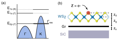
To understand the experimental observations, we carried out theoretical calculations of acceptor impurities in WS2 using a recently developed approach that allows the simulation of very large supercells that are required to accurately describe shallow defect states of charged impurities [16]. In particular, we first calculated the screened potential of the defect, which is modelled as a point charge with located above the plane of the tungsten atoms, see Fig. 2(b). To describe the screening of the defect charge, the dielectric function of the system is computed using the random phase approximation (RPA). For this, we compute the polarizability as the sum of contributions from the WS2, the doped graphene and the SiC substrate (see SM for details [27]).
To calculate the LDOS of a single charged impurity in WS2, we carry out large-scale tight-binding calculations using a three-band tight-binding model [29] with the screened defect potential included as an on-site energy [16]. This allows us to obtain converged results for a WS2 supercell. This supercell, which would be extremely challenging to model with ab initio techniques, is sufficiently large to capture the decay of the shallow impurity states and obtain accurate defect state energies. While this approach allows us to describe states induced by the long-ranged screened defect potential, the model does not capture short-ranged chemical interactions that could give rise to additional defect states.
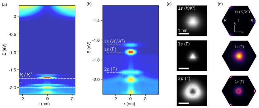
Figures 3(a) and (b) show the calculated LDOS of a single acceptor impurity in WS2. In agreement with the measured map [Fig. 1(c)], we observe a significant defect-induced upward bending of the conduction band edge. In the vicinity of the valence band edge, a series of defect states are found. Fig. 3(c) shows the simulated STM images of the three most strongly bound defect states that give rise to significant peaks in the LDOS (see SM for details of STM simulations [27]). The two most strongly bound states appear similar to experimental states A and B as circular bright spots with a similar size [Fig. 1(f)]. The binding energies with respect to the valence band maximum at K/K′ of these states are 95 meV and 25 meV, respectively. While the absolute binding energies are somewhat smaller than the experimental values, see Table 1, their difference (70 meV) is in good agreement with experiment (80 meV). As these states exhibit symmetries similar to the eigenstates of the two-dimensional hydrogen atom, we label them as states. Interestingly, we find that the more strongly bound state is less localized than the other state. At lower binding energies, a -like defect state is found that is characterized by a node at its center. This state resembles the state C in Fig. 1(f). The binding energy of this states is meV indicating that it lies between and K/K′. Again, we find that the binding energy difference between this state and the less strongly bound state is in very good agreement with experiment (theory: 205 meV, experiment: 225 meV).
To understand which band extrema these defect states originate from, we decompose the defect wave functions into contributions from unperturbed WS2 states. Fig. 3(d) shows that the most strongly bound defect state originates from the K valley (a second degenerate state with opposite spin originates from the K′ valley) and is therefore labelled as (K), while the other state originates from the valley. As the effective mass of the valley is larger than that of the K/K′ valleys, the () state is more localized despite being less strongly bound [recall that for the 2D hydrogen atom indicating that a larger electron mass results in a more localized state]. The analysis of the resonance reveals that this impurity level mostly originates from unperturbed states in the vicinity of , but also has contributions from a few states near K (note that mixing only occurs between states with the same spin preventing any hybridization with states from K′). The valley hybridization is a consequence of the resonant nature of the defect state and can be understood within the framework of effective mass theory [3]. In this approach, one first neglects the coupling between different valleys and obtains a set of bound defect states for each valley. When the coupling between valleys is turned on, the bound states from the secondary valence band extremum at that lie in the same energy range as continuum states from the K and K′ valleys can mix with the continuum states. The resulting hybridized states can be expressed as
| (1) |
where and denote the bound and continuum states obtained for decoupled valleys, respectively, (with labelling the valley), and are complex coefficients, and denotes the k-space region corresponding to the valley.
Finally, we discuss the effect of resonant impurities on electron transport. If a hole near one of the primary band extrema (i.e., in the K or K′ valley) in an external electric field reaches the energy of the resonant impurity state , it does not participate in conduction for a time . Here, denotes the width of the resonant impurity level given by
| (2) |
where denotes the energy of a continuum state with crystal momentum in valley and is the matrix element of the Bloch-transformed screened impurity potential between and [3]. Evaluating this expression with our first-principles defect potential and tight-binding wave functions yields meV and ps. This result shows that resonant defect states exhibit extremely small linewidths corresponding to long trapping times. Thus, we predict that resonant states should lead to a drastic reduction in conductivity when the Fermi level reaches the resonant impurity level. Note that in a WS2 transport device, graphene could not be used as substrate as most carriers would propagate through the graphene. Without graphene, the screening of the impurity charge would be reduced, resulting in a resonant impurity level that lies closer to the VBM at K/K′. The trapping time, however, would not change significantly as a consequence of the flat density of state of WS2 near the VBM.
In this Letter, we have studied the localized acceptor states associated with negatively charged point defects in WS2 using scanning tunneling microscopy and spectroscopy. We identify these states as resonant and bound hydrogenic states of the screened Coulomb potential. Our large-scale atomistic electronic structure calculations reproduce the band bending and binding energies of the defect states as well as their wave function shapes and sizes as observed in STS measurements. The hydrogenic states exhibit - and -type character and originate from both the K/K′ and valence band valleys. Despite the hybridization with the primary valence bands around K and K′, the resonant state emerging from is clearly resolved. We further predict that resonant states can trap mobile carriers for up to 30 picoseconds. Our findings highlight the importance of a detailed understanding of the effect of charged defects for the development of novel nano-electronic devices based on two-dimensional semiconductors.
Acknowledgments: This work was supported through a studentship in the Centre for Doctoral Training on Theory and Simulation of Materials at Imperial College London funded by the EPSRC (EP/L015579/1). We acknowledge the Thomas Young Centre under grant number TYC-101. Via J.L.’s membership of the UK’s HEC Materials Chemistry Consortium, which is funded by EPSRC (EP/L000202, EP/R029431), this work used the ARCHER UK National Supercomputing Service (http://www.archer.ac.uk). The work performed at the Molecular Foundry was supported by the Office of Science, Office of Basic Energy Sciences, of the U.S. Department of Energy under Contract No. DE-AC02-05CH11231. B.S. appreciates support from the Swiss National Science Foundation under project number P2SKP2_171770. A.W.-B. was supported by the U.S. Department of Energy Early Career Award. J.-H.L. and J.B.N. were supported by the Air Force Office of Scientific Research Hybrid Materials MURI under award number FA9550-18-1-0480. Computational resources for performing the ab initio calculations were provided by the National Energy Research Scientific Computing Center and the Molecular Foundry, DOE Office of Science User Facilities supported by the Office of Science of the U.S. Department of Energy under Contract No. DE-AC02-05CH11231.
References
- Sun et al. [2014] J. Sun, Z. Yu, Y. Huang, Y. Xia, W. S. Lai, and H. Gong, Significant improvement in electronic properties of transparent amorphous indium zinc oxide through yttrium doping, EPL (Europhysics Letters) 106, 17006 (2014).
- Van de Walle et al. [2010] C. G. Van de Walle, J. L. Lyons, and A. Janotti, Controlling the conductivity of inn, Physica Status Solidi (a) 207, 1024 (2010).
- Bassani et al. [1974] F. Bassani, G. Iadonisi, and B. Preziosi, Electronic impurity levels in semiconductors, Reports on Progress in Physics 37, 1099 (1974).
- Xie et al. [2017] Z. Xie, Y. Sui, J. Buckeridge, C. R. A. Catlow, T. W. Keal, P. Sherwood, A. Walsh, D. O. Scanlon, S. M. Woodley, and A. A. Sokol, Demonstration of the donor characteristics of si and o defects in gan using hybrid qm/mm, physica status solidi (a) 214, 1600445 (2017).
- Zhang et al. [2013] G. Zhang, A. Canning, N. Grønbech-Jensen, S. Derenzo, and L.-W. Wang, Shallow impurity level calculations in semiconductors using ab initio methods, Phys. Rev. Lett. 110, 166404 (2013).
- Bastard [1981] G. Bastard, Hydrogenic impurity states in a quantum well: A simple model, Phys. Rev. B 24, 4714 (1981).
- Karazhanov et al. [2003] S. Z. Karazhanov, Y. Zhang, L.-W. Wang, A. Mascarenhas, and S. Deb, Resonant defect states and strong lattice relaxation of oxygen vacancies in , Phys. Rev. B 68, 233204 (2003).
- Kohn [1957] W. Kohn, Shallow impurity states in silicon and germanium, Solid State Physics 5, 257 (1957).
- Louie et al. [1976] S. G. Louie, M. Schluter, J. R. Chelikowsky, and M. L. Cohen, Self-consistent electronic states for reconstructed si vacancy models, Phys. Rev. B 13 (1976).
- Yu et al. [2018] H. Yu, A. R. Shaikh, F. Xiong, and Y. Chen, Enhanced out-of-plane electrical transport in n-type snse thermoelectrics induced by resonant states and charge delocalization, ACS Applied Materials & Interfaces 10, 9889 (2018).
- Zhang et al. [2012] Q. Zhang, H. Wang, W. Liu, H. Wang, B. Yu, Q. Zhang, Z. Tian, G. Ni, S. Lee, K. Esfarjani, G. Chen, and Z. Ren, Enhancement of thermoelectric figure-of-merit by resonant states of aluminium doping in lead selenide, Energy Environ. Sci. 5, 5246 (2012).
- Kormányos et al. [2014] A. Kormányos, V. Zólyomi, N. D. Drummond, and G. Burkard, Spin-orbit coupling, quantum dots, and qubits in monolayer transition metal dichalcogenides, Phys. Rev. X 4, 011034 (2014).
- Baugher et al. [2014] B. W. H. Baugher, H. O. H. Churchill, Y. Yang, and P. Jarillo-Herrero, Optoelectronic devices based on electrically tunable p-n diodes in a monolayer dichalcogenide, Nature Nanotechnology 9, 262 (2014).
- Mak et al. [2010] K. F. Mak, C. Lee, J. Hone, J. Shan, and T. F. Heinz, Atomically thin : A new direct-gap semiconductor, Phys. Rev. Lett. 105, 136805 (2010).
- Qiu et al. [2013] D. Y. Qiu, F. H. da Jornada, and S. G. Louie, Optical spectrum of : Many-body effects and diversity of exciton states, Phys. Rev. Lett. 111, 216805 (2013).
- Aghajanian et al. [2018] M. Aghajanian, A. A. Mostofi, and J. Lischner, Tuning electronic properties of transition-metal dichalcogenides via defect charge, Scientific Reports 6, 1 (2018).
- Kastl et al. [2017] C. Kastl, C. T. Chen, T. Kuykendall, B. Shevitski, T. P. Darlington, N. J. Borys, A. Krayev, P. J. Schuck, S. Aloni, and A. M. Schwartzberg, The important role of water in growth of monolayer transition metal dichalcogenides, 2D Mater. 4, 021024 (2017).
- Schuler et al. [2019a] B. Schuler, J.-H. Lee, C. Kastl, K. Cochrane, C. T. Chen, S. Refaely-Abramson, S. Yuan, E. van Veen, R. Roldan, N. Borys, R. J. Koch, T. Seyller, S. Aloni, A. M. Schwartzberg, D. F. Ogletree, J. B. Neaton, and A. Weber-Bargioni, How substitutional point defects in two-dimensional \ceWS2 induce charge localization, spin-orbit splitting, and strain, ACS Nano , (in press) (2019a).
- Liu et al. [2016] X. Liu, I. Balla, H. Bergeron, and M. C. Hersam, Point defects and grain boundaries in rotationally commensurate MoS2 on epitaxial graphene, J. Phys. Chem. C. 120, 20798 (2016).
- Lin et al. [2018] Y.-C. Lin, B. Jariwala, B. M. Bersch, K. Xu, Y. Nie, B. Wang, S. M. Eichfeld, X. Zhang, T. H. Choudhury, Y. Pan, et al., Realizing large-scale, electronic-grade two-dimensional semiconductors, ACS Nano 12, 965 (2018).
- Le Quang et al. [2018] T. Le Quang, K. Nogajewski, M. Potemski, M. T. Dau, M. Jamet, P. Mallet, and J. Veuillen, Band-bending induced by charged defects and edges of atomically thin transition metal dichalcogenide films, 2D Mater. 5, 035034 (2018).
- Addou et al. [2015] R. Addou, L. Colombo, and R. M. Wallace, Surface defects on natural , ACS Applied Materials & Interfaces 7, 11921 (2015).
- Gross et al. [2009] L. Gross, F. Mohn, N. Moll, P. Liljeroth, and G. Meyer, The chemical structure of a molecule resolved by atomic force microscopy, Science 325, 1110 (2009).
- Ulstrup et al. [2019] S. Ulstrup, C. E. Giusca, J. A. Miwa, C. E. Sanders, A. Browning, P. Dudin, C. Cacho, O. Kazakova, D. K. Gaskill, R. L. Myers-Ward, et al., Nanoscale mapping of quasiparticle band alignment, Nat. Commun. 10, 3283 (2019).
- Schuler et al. [2019b] B. Schuler, D. Y. Qiu, S. Refaely-Abramson, C. Kastl, C. T. Chen, S. Barja, R. J. Koch, D. F. Ogletree, S. Aloni, A. M. Schwartzberg, et al., Large spin-orbit splitting of deep in-gap defect states of engineered sulfur vacancies in monolayer WS2, Phys. Rev. Lett. , (in press) (2019b).
- Zhang et al. [2008] Y. Zhang, V. W. Brar, F. Wang, C. Girit, Y. Yayon, M. Panlasigui, A. Zettl, and M. F. Crommie, Giant phonon-induced conductance in scanning tunnelling spectroscopy of gate-tunable graphene, Nature Physics 4, 627 (2008).
- [27] Supplemental Material available at https://… .
- Qiu et al. [2017] Z. Qiu, H. Fang, A. Carvalho, A. Rodin, Y. Liu, S. J. Tan, M. Telychko, P. Lv, J. Su, Y. Wang, et al., Resolving the spatial structures of bound hole states in black phosphorus, Nano Lett. 17, 6935 (2017).
- Liu et al. [2015] G. Liu, D. Xiao, Y. Yao, X. Xu, and W. Yao, Electronic structure and theoretical modelling of two-dimensional group-VIB transition metal dichalcogenides, Chem. Soc. Rev. 44, 2643– (2015).