Superconductivity of Electron-Doped NdOBiS2 by Substitution of Mixed-Valence Ce ions
Abstract
Superconductivity is achieved in Nd1-xCexOBiS2 via electron doping using mixed-valence Ce ions. Single crystals with x = 0.2, 0.3, 0.4, and 0.5 are generated using a CsCl flux method. Plate-like single crystals with dimensions of 0.80.80.2 mm3 were obtained. The magnetic susceptibility indicates large diamagnetism, and the electrical resistivity indicates zero resistivity. The maximum value of is observed at 4.7 K in Nd0.8Ce0.2OBiS2 from . From the measurements taken in several magnetic fields, the upper critical field (0) is estimated to be 12 and 0.34 T for the - and -planes, respectively. We redetermined of NdO0.7F0.3BiS2, as 35 and 0.78 T for the - and -planes, respectively. The anisotropic parameter is estimated to be 35 for Nd0.7Ce0.3OBiS2 and 45 for NdO0.7F0.3BiS2. The (0) of Nd0.7Ce0.3OBiS2 is approximately two times smaller than that of NdO0.7F0.3BiS2, although the difference of is approximately 10.
The newly discovered BiS2-based superconductors Bi4O4S3 and RO1-xFxBiS2 (R = La, Ce, Pr, Nd) are of interest owing to their various crystal structures similar to those in layered cuprate and iron pnictide superconductors[1, 2, 3, 4, 5, 6, 7, 8, 9]. The crystal structure of the BiCh2-based (Ch: chalcogen) superconductors consists of alternating stacks of RO-blocking and BiCh2 conducting layers. It is known that electron carrier doping into the conduction band, mainly comprising Bi-6 and Ch- orbitals[10, 11], induces superconductivity in the BiS2-based compounds. Recent research has indicated that in-plane chemical pressure is related to the overlapping of the Bi-6 and Ch- orbitals, which is a significant contributor to bulk superconductivity[12]. A typical approach to increasing overlapping is by substituting elements with a longer ionic radius (e.g. Se substitution for S sites)[13, 14, 15]. From detailed analysis of the crystal structure, the chemical pressure effects effectively ameliorated the in-plane disorder in the BiCh2 conducting layer[16, 17, 18, 19].
The mechanism of superconductivity in BiS2-based compounds has received attention but remains under debate. The specific heat measurements of a bulk superconductor of LaO0.5F0.5BiSSe suggest full gap symmetry and indicate that superconductivity is mediated by electron–phonon coupling[20, 21]. However, the Se isotope effect suggests that the superconducting pairing interaction may not be due to electron–phonon interaction[22]. In a single crystal of Nd(O,F)BiS2, penetration depth and thermal conductivity indicate that superconductivity is a full-gap symmetry[23, 24, 25]. In contrast, recent angle-resolved photoemission spectroscopy (ARPES) measurements suggest that the superconducting gap of NdO0.71F0.29BiS2 is anisotropic[26]. Thus, the mechanism of the BiS2-based superconductor is still controversial.
As previously mentioned, electron doping is necessary to induce bulk superconductivity in BiS2-based compounds. Recently, superconductivity has been observed in non-substituted CeOBiS2; this is mostly because of electron doping by mixed-valence Ce ions[27]. The compound is considered to have the mixed valence of Ce3+/Ce4+. In addition, superconductivity in the non-F-substituted LaOBiSSe and PrOBiS2 is achieved by Ce-substitution at R-sites, suggesting that the carriers are injected owing to the mixed valence of Ce3+/Ce4+[28, 29]. These results indicate that substitution by mixed-valence Ce ions can effectively induce superconductivity.
The investigation of superconductivity induced by electron doping except for F helps in a better understanding of the mechanism. Because F-substituted NdOBiS2 is known to exhibit the highest superconducting transition temperature () in the ROBiS2 compounds at ambient pressure[5, 30], a higher is highly desirable in NdOBiS2 by Ce-substitution. In the present study, we have successfully generated single crystals of Nd1-xCexOBiS2 and reported the discovery of superconductivity in Nd1-xCexOBiS2 through electrical resistivity and magnetic susceptibility measurements. From the results, we revealed the superconducting properties of Nd1-xCexOBiS2. We noted that of the crystals grown using the 99.9%- and 99.999%-CsCl fluxes were similar[31]. In other words, we confirmed that the F impurity in 99.9%-CsCl flux is not the primary factor in electron doping to induce superconductivity.
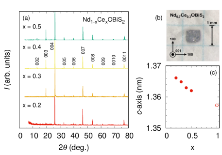
Single crystals of Nd1-xCexOBiS2 with x = 0.2, 0.3, 0.4, and 0.5 were synthesized by a CsCl-flux method. The nominal compositions of Nd2O3 (99.9%, Kojundo Chemical Lab. Co.), Nd2S3 (99%, Kojundo Chemical Lab. Co.), CeO2 (99%, Kojundo Chemical Lab. Co.), and Bi2S3 (99.9%, Kojundo Chemical Lab. Co.) were weighed (total mass of 0.8 g) and mixed with 5 g of CsCl powder (99.999%, Kojundo Chemical Lab. Co.). The mixture was sealed in an evacuated quartz tube. The quartz tube underwent heating at 950 ℃ for 10 h followed by cooling to 650 ℃ at a rate of 1 ℃/h; then, the sample was cooled to room temperature in the furnace. We successfully synthesized single crystals of Nd1-xCexOBiS2 with x = 0.2, 0.3, 0.4, and 0.5. As shown in Fig. 1(b), the plate-like crystals were grown with x = 0.3, 0.4, and 0.5, and the typical dimensions are approximately 0.80.80.2 mm3. The shape of the generated crystal with x = 0.2 is slightly lumpy and small. A single crystal with x = 0.1 was not generated at this stage. The results indicate that single crystals with low carrier doping are difficult to generate, and non-doped NdOBiS2 could not be successfully synthesized[5, 30].
The crystal structure was verified through X-ray diffraction (XRD), which employed a conventional X-ray spectrometer equipped with Cu-K radiation (RINT 2500, Rigaku). The chemical composition of the single crystals of Nd1-xCexOBiS2 was analyzed by X-ray fluorescence (XRF), conducted using a JEOL JSX 1000S ElementEye. Electrical resistivity was measured via a standard dc-four-probe method. Electrical connections with the sample comprised gold wires ( = 25 m) joined with Ag paste (4922N, DuPont). DC-magnetic susceptibility was measured by a magnetic property measurement system (MPMS, Quantum Design), down to 2.0 K. AC-electrical resistivity was measured by a physical property measurement system (PPMS, Quantum Design), down to 2.0 K in magnetic fields of several intensities, including zero. Thermoelectric power was measured using a seesaw heating method by considering a different temperature of about 1 K. Thermoelectric voltage was measured by a nano-voltmeter (2182A, Keithley).
Figure 1(a) shows the XRD patterns of the single crystalline sample of Nd1-xCexOBiS2 along the -axis at room temperature. The presence of only 00 diffraction peaks indicates that the -plane is well grown. Figure 1(c) shows that the lattice constant was 1.3661 nm for Nd0.8Ce0.2OBiS2, and decreased as Ce content x increased. The result conflicts with lanthanide contraction for a trivalent Ce valence, because the ionic radius of Nd3+ is smaller than that of Ce3+. However, the lattice constants of CeOBiS2 are slightly smaller than those of LaOBiS2 and PrOBiS2, indicating that the Ce valence is a mixed state of Ce3+/Ce4+[27]. Thus, the shrinking of the lattice constants of the Ce-substituted NdOBiS2 indicates the presence of Ce4+.
The XRF analysis helped determine the chemical composition ratios of the single crystals for x = 0.2, 0.3, 0.4, and 0.5, which were Nd0.73Ce0.24BiS1.7, Nd0.72Ce0.30BiS1.9, Nd0.59Ce0.41BiS2.0, and Nd0.57Ce0.53BiS2.1, respectively. The O composition ratio could not be determined. The values suggest that the chemical composition of the grown crystals is almost consistent with the nominal one, although the ratio of x = 0.5 is slightly deviated. The ratio of the single crystal for x = 0.2 seems to indicate a lack of S. One possible explanation is that the deviation is ascribed to the lumpy shape, which causes a measurement error. Another possibility is that a lack of S leads to the lumpy shape.
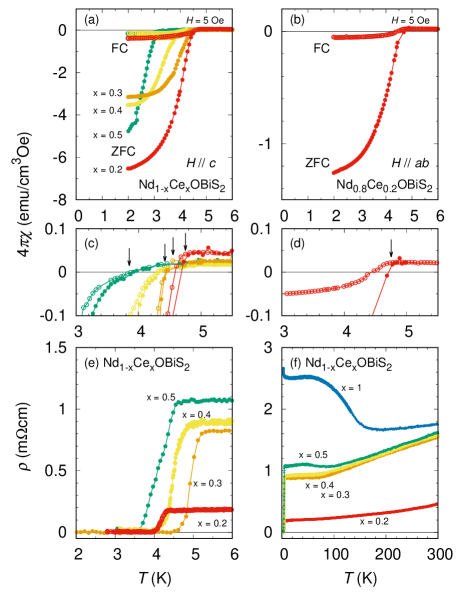
Figures 2(a-b) show the -dependence of the magnetic susceptibility of Nd1-xCexOBiS2 on heating after zero-field cooling (ZFC) and then on cooling in the field (field cooling, FC) for and . A large diamagnetism was observed in Nd1-xCexOBiS2 (x = 0.2, 0.3, 0.4, and 0.5). The significant exceedance of 4 is due to the diamagnetic factor when was applied along the -axis. By applying a magnetic field along the -plane, the diamagnetic factor is almost negligible. Figure 2(b) shows that a large diamagnetism was observed in Nd0.8Ce0.2OBiS2 at 4.7 K, suggesting that the superconductivity is of bulk nature, although the shielding effect slightly exceeds 1 in 4. It is likely that the roughness of the crystal shape leads to the misalignment of the field applied to the -plane.
Figures 2(c-d) show that is defined as the temperature where the magnetization drop starts to appear. Because for x = 0.5 gradually decreases, we consider as the temperature where FC starts to deviate from the ZFC. The values obtained for are 4.75 (x = 0.2), 4.55 (x = 0.3), 4.42 (x = 0.4), and 3.85 K (x = 0.5). slightly decreases with increasing x. This behavior corresponds to the F-doped NdOBiS2[5], which exhibits the highest (= 5.2 K) at ambient pressure. In addition, the maximum of the Ce-doped compounds is slightly lower than that of NdO1-xFxBiS2[5]. Such behavior is also observed in Ce-doped LaOBiSSe and PrOBiS2[28, 29]. The origin of the difference in is not clear.
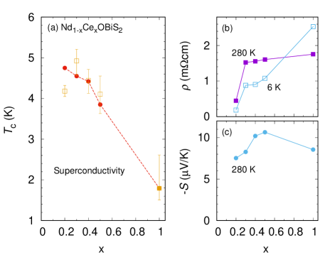
Figures 2(e-f) show the -dependence of the electrical resistivity of Nd1-xCexOBiS2 at low temperatures. Superconductivity was confirmed by in all the samples. obtained from was determined as the temperature of 50%, where is the residual resistivity. The error bar as the superconducting transition width of and is defined as 98% and 2%. The values obtained for are 4.18 (x = 0.2), 4.92 (x = 0.3), 4.47 (x = 0.4), and 4.11 K (x = 0.5). Nd0.7Ce0.3OBiS2 exhibits the highest among the Ce-doped compounds, where is almost consistent with obtained from . for x = 0.2 obtained from differs from that of . This could be owing to the Joule heat caused when current was applied in an extremely small sample. A superconducting phase diagram summarizes the above in Fig. 3(a).
Figure 2(f) shows the -dependence of the electrical resistivity of Nd1-xCexOBiS2 down to 3.0 K. A large hump was observed in of non-doped CeOBiS2 at approximately 130 K. The result corresponds to the previous report[27]. Metallic behavior was observed when x = 0.2, 0.3, 0.4, and 0.5, indicating that the electron carriers were doped with the mixed-valence state of the Ce ion. At x = 0.5, a small hump was observed at approximately 80 K and was greatly suppressed from the non-doped compound. Figure 3(b) shows the values of (6 K) and (280 K) plotted. Both (6 K) and (280 K) increase with the Ce content x.
To understand the carrier density of the Ce-doped NdOBiS2, we measured the Seebeck coefficient at 280 K, as shown in Fig. 3(c). In metals or degenerate semiconductors (single parabolic band and energy-independent scattering approximation)[32, 33], is proportional to 1/, where is the carrier concentration. The absolute value of in x = 0.2 is 7.4 V/K, which is the smallest value in the Ce-doped NdOBiS2. With an increase in the Ce content x, the absolute value increases, which corresponds to the increase in (280 K). The results show a decrease in the carrier density despite the increase in the amount of Ce substitution. The behavior can be understood by the changing ratio of Ce3+/Ce4+ depending on the substitution amount, and the ratio of Ce4+ increases as the x value decreases. In contrast, when the Ce concentration is further increased above = 0.5, the absolute value of decreases. The decreasing conflicts with the behavior in CeOBiS2. Because the anomaly of is not similar to the metallic or semiconducting behavior, there is a possibility that the assumption of the metals or degenerate semiconductors is inadequate in CeOBiS2.
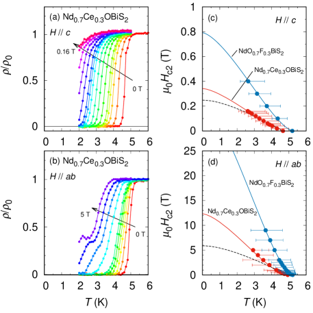
Figures 4(a-b) show of Nd0.7Ce0.3OBiS2 in several magnetic fields applied along with and . The upper critical field of Nd0.7Ce0.3OBiS2 is obtained from the measurements in several magnetic fields, as shown in Figs. 4(c-d). The superconductivity is significantly suppressed with increasing magnetic fields in both directions. above 3 T shows a small hump at a low temperature point, which is not reproducible. It is likely that the behaviors are not intrinsic. As shown in Figs. 4(c-d), the dotted lines show the Werthamer–Helfand–Hohenberg (WHH) theory prediction[34, 35]. In both curves, the curves deviate from the WHH prediction and exhibit a positive curvature at around . This behavior is mainly attributed to spin-orbit coupling[35], multi-gap superconductivity[36, 37], and strong electron–phonon coupling[38, 39]. However, the origin of the positive curvature in the BiS2-based superconductors still remains to be clarified. A reasonable fit to the data for Nd0.7Ce0.3OBiS2 can be obtained using the expression = (0)[1 − ()3/2]3/2[40]. This model was also used to fit for BiS2-based superconductors[20, 41], (Zr, Hf)IrSi[42], Nb0.18Re0.82[43], WRe3[44], PbTaSe2[45], and high-entropy alloys[46]. was determined as 12 T for the and 0.34 T for the -axis. In this article, we redetermined of NdO0.7F0.3BiS2 from the same definition of , as shown in Figs. 4(c-d). The data were taken from the previous report[30]. was determined as 35 T for the and 0.78 T for the -axis. These values are clearly larger than those of the Ce-doped NdOBiS2. The results indicate that the for both directions reduces in superconductivity induced by the Ce-doping. Because measurements were performed above 2.0 K and above 9 T, lower temperature and higher field measurements were needed to determine the accurate values of the F- and Ce-doped NdOBiS2.
The anisotropic parameter was determined using the anisotropic Ginzburg–Landau (GL) formula,
| (1) |
where , are the effective masses, and , are the GL-coherence lengths. and were evaluated using = /(2) and = /(2), where is the quantum flux. and were obtained as 86 and 0.31 nm for Nd0.7Ce0.3OBiS2, respectively. The anisotropic parameter was estimated to be 35. The result suggests that the superconductivity possesses high anisotropy. The of NdO0.7F0.3BiS2 was recalculated to be 45. Because the difference in is approximately 10, there is no considerable difference between F-doped and Ce-doped NdOBiS2.
In summary, we succeeded in growing a single crystal of Nd1-xCexOBiS2 (x = 0.2, 0.3, 0.4, and 0.5). Plate-like single crystals with dimensions of 0.80.80.2 mm3 were obtained. We discovered bulk superconductivity at = 4.7 K in a compound with x = 0.2. The lattice constant of the -axis decreased with an increase in Ce content x. The shrinking of the -axis indicated the mixed valency of Ce3+/Ce4+. It is likely that the superconductivity of Nd1-xCexOBiS2 was induced by the electron doping of the mixed valence of Ce3+/Ce4+. The superconducting transition temperature of Ce-substituted Nd1-xCexOBiS2 was slightly lower than that of F-substituted NdO1-xFxBiS2. This tendency is also observed in Ce-substituted La1-xCexOBiSSe and Ce1-xPrxOBiS2. of Nd1-xCexOBiS2 showed a metallic behavior. In a compound with x = 0.5, a broad hump was observed in at approximately 80 K, similar to that found in CeOBiS2. The electrical resistivity of (6 K) and (280 K) increased with increasing x. The tendency of can be understood by the increase of the Ce4+ ratio with decreasing Ce content below x = 0.5. The upper critical field of Nd0.7Ce0.3OBiS2 was determined to be 12 T for and 0.34 T for -axis. The anisotropic parameter was estimated to be 35, which was comparable to that of F-doped NdOBiS2. The (0) of the Ce-doped NdOBiS2 was approximately two times smaller than that of the F-doped one, although the difference of was approximately 10. The results imply that the for both directions reduces in superconductivity induced by Ce-doping. Our results for Ce-doped NdOBiS2 make it possible to help understand superconductivity in BiS2-based superconductors.
Acknowledgment
This work was partially supported by the Kurata Grants from the Hitachi Global Foundation, Izumi Science and Technology Foundation, and Casio Science Promotion Foundation. The authors would like to thank Prof. Ryuji Tamura for his help in measuring the XRF data. DC-magnetic susceptibility performed by MPMS and electrical resistivity in magnetic fields by PPMS were carried out in collaboration with the Institute for Solid State Physics, University of Tokyo.
References
- [1] Y. Mizuguchi, H. Fujishita, Y. Gotoh, K. Suzuki, H. Usui, K. Kuroki, S. Demura, Y. Takano, H. Izawa, and O. Miura, Phys. Rev. B, 86, 220510(R) (2012).
- [2] Y. Mizuguchi, S. Demura, K. Deguchi, Y. Takano, H. Fujishita, Y. Gotoh, H. Izawa, and O. Miura, J. Phys. Soc. Jpn., 81, 114725 (2012).
- [3] J. Xing, S. Li, X. Ding, H. Yang, and H.-H. Wen, Phys. Rev. B, 86, 214518 (2012).
- [4] D. Yazici, K. Huang, B. D. White, A. H. Chang, A. J. Friedman, and M. B. Maple, Philos. Mag., 93, 673 (2013).
- [5] S. Demura, Y. Mizuguchi, K. Deguchi, H. Okazaki, H. Hara, T. Watanabe, S. J. Denholme, M. Fujioka, T. Ozaki, H. Fujihisa, J. Phys. Soc. Jpn., 82, 033708 (2013).
- [6] R. Jha, A. Kumar, S. Kumar Singh, and V. P. S. Awana, J. Supercond. Nov. Magn., 26, 499 (2013).
- [7] X. Lin, X. Ni, B. Chen, X. Xu, X. Yang, J. Dai, Y. Li, X. Yang, Y. Luo, Q. Tao, G. Cao, and Z. Xu, Phys. Rev. B 87, 020504(R) (2013)
- [8] R. Jha, B. Tiwari, and V. P. S. Awana, J. Applied Physics 117, 013901 (2015).
- [9] R. Jha, B. Tiwari, and V. P. S. Awana, J. Phys. Soc. Jpn., 83, 063707 (2014).
- [10] H. Usui, K. Suzuki, and K. Kuroki, Phys. Rev. B 86, 220501 (2012).
- [11] H. Usui and K. Kuroki, Nov. Supercond. Mater., 1, 50 (2015).
- [12] Y. Mizuguchi, A. Miura, J. Kajitani, T. Hiroi, O. Miura, K. Tadanaga, N. Kumada, E. Magome, C. Moriyoshi, and Y. Kuroiwa, Sci. Rep. 5, 14968 (2015).
- [13] T. Hiroi, J. Kajitani, A. Omachi, O. Miura, and Y. Mizuguchi, J. Phys. Soc. Jpn. 84, 024723 (2015).
- [14] G. Jinno, R. Jha, A. Yamada, R. Higashinaka, T. D. Matsuda, Y. Aoki, M. Nagao, O. Miura, and Y. Mizuguchi, J. Phys. Soc. Jpn. 85, 124708 (2016).
- [15] Y. Goto, R. Sogabe, and Y. Mizuguchi, J. Phys. Soc. Jpn. 86, 104712 (2017).
- [16] E. Paris, B. Joseph, A. Iadecola, T. Sugimoto, L. Olivi, S. Demura, Y. Mizuguchi, Y. Takano, T. Mizokawa, and N. L. Saini, J. Phys.: Condens. Matter, 26 435701 (2014).
- [17] Y. Mizuguchi, E. Paris, T. Sugimoto, A. Iadecola, J. Kajitani, O. Miura, T. Mizokawa and N. L. Saini, Phys. Chem. Chem. Phys. 17, 22090 (2015).
- [18] A. Athauda, J. Yang, S. Lee, Y. Mizuguchi, K. Deguchi, Y. Takano, O. Miura, and D. Louca, Phys. Rev. B 91, 144112 (2014).
- [19] K. Nagasaka, A. Nishida, R. Jha, J. Kajitani, O. Miura, R. Higashinaka, T. D. Matsuda, Y. Aoki, A. Miura, C. Moriyoshi, Y. Kuroiwa, H. Usui, K. Kuroki, and Y. Mizuguchi, J. Phys. Soc. Jpn. 86, 074701 (2017).
- [20] N. Kase, Y. Terui, T. Nakano, and N. Takeda, Phys. Rev. B 96, 214506 (2017).
- [21] N. Kase, J. Phys. Soc. Jpn., 88, 041007 (2019).
- [22] K. Hoshi, Y. Goto, and Y. Mizuguchi, Phys. Rev. B 97, 094509 (2018).
- [23] L. Jiao, Z. Weng, J. Liu, J. Zhang, G. Pang, C. Guo, F. Gao, X. Zhu, H.-H. Wen, and H. Q. Yuan, J. Phys.: Condens. Matter 27, 225701 (2015).
- [24] Shruti, S. P. Srivastava, and S. Patnaik, J. Phys.: Condens. Matter 25, 312202 (2013).
- [25] T. Yamashita, Y. Tokiwa, D. Terazawa, M. Watauchi, I. Tanaka, T. Terashima, and Y. Matsuda, J. Phys. Soc. Jpn. 85, 073707 (2016).
- [26] Y. Ota, K. Okazaki, H. Q. Yamamoto, T. Yamamoto, S. Watanabe, C. Chen, M. Nagao, S. Watauchi, I. Tanaka, Y. Takano, and S. Shin, Phys. Rev. Lett. 118, 167002 (2017).
- [27] M. Tanaka, M. Nagao, R. Matsumoto, N. Kataoka, I. Ueta, H. Tanaka, S. Watauchi, I. Tanaka, and Y. Takano, J. Alloys Compd., 722, (2017) 467.
- [28] R. Sogabe, Y. Goto, A. Nishida, T. Katase, and Y. Mizuguchi, EPL, 122, (2018) 17004.
- [29] A. Miura, M. Nagao, Y. Goto, Y. Mizuguchi, T. D. Matsuda, Y. Aoki, C. Moriyoshi, Y. Kuroiwa, Y. Takano, S. Watauchi, I. Tanaka, N. C. Rosero-Navarro, and K. Tadanaga, Inorg. Chem. 57, 5364-5370 (2018).
- [30] M. Nagao, S. Demura, K. Deguchi, A. Miura, S. Watauchi, T. Takei, Y. Takano, N. Kumada, and I. Tanaka, J. Phys. Soc. Jpn., 82, 113701 (2013).
- [31] (Supplemental material) Detailed results of the electrical resistivity are provided online.
- [32] M. Cutler, J. F. Leavy, and R. L. Fitzatrick, Phys. Rev., 133 (1964) A1143.
- [33] G. J. Snyder and E. S. Toberer, Nat. Mater., 7, 105-114 (2008).
- [34] K. Maki, Phys. Rev., 148, (1966) 362.
- [35] E. Helfand and N. R. Werthamer, Phys. Rev., 147, (1966) 288.
- [36] Y. Nakajima, H. Hidaka, T. Nakagawa, T. Tamegai, T. Nishizaki, T. Sasaki, N. Kobayashi, Phys. Rev. B 85, 174524 (2012).
- [37] Y. C. Chan, K. Y. Yip, Y. W. Cheung, Y. T. Chan, Q. Niu, J. Kajitani, R. Higashinaka, T. D. Matsuda, Y. Yanase, Y. Aoki, K. T. Lai, and Swee K. Goh, Phys. Rev. B 97, 104509 (2018).
- [38] L. N. Bulaevskii, O. V. Dolgov, and M. O. Ptitsyn, Phys. Rev. B, 38, 11290 (1988).
- [39] F. Marsiglio and J. P. Carbotte, Phys. Rev. B 41, 8765 (1990).
- [40] R. Micnas, J. Ranninger, and S. Robaszkiewicz, Rev. Mod. Phys., 62, 113 (1990).
- [41] P. K. Biswas, A. Amato, C. Baines, R. Khasanov, H. Luetkens, H. Lei, C. Petrovic, and E. Morenzoni, Phys. Rev. B 88, 224515 (2013).
- [42] N. Kase, H. Suzuki, T. Nakano, and N. Takeda, Supercond. Sci. Technol. 29, 035011 (2016).
- [43] A. B. Karki, Y. M. Xiong, N. Haldolaarachchige, S. Stadler, I. Vekhter, P. W. Adams, D. P. Young, W. A. Phelan, and J. Y. Chan, Phys. Rev. B 83, 144525 (2011).
- [44] P. K. Biswas, M. R. Lees, A. D. Hillier, R. I. Smith, W. G. Marshall, and D. McK. Paul, Phys. Rev. B 84, 184529 (2011).
- [45] M. N. Ali, Q. D. Gibson, T. Klimczuk, and R. J. Cava, Phys. Rev. B, 89, 020505 (2014).
- [46] K. Stolze, J. Tao, F. O. von Rohr, T. Kong, and R. J. Cava, Chem. Mater. 30, 906-914 (2018).