Millimeter-Wave Four-Wave Mixing via Kinetic Inductance for Quantum Devices
Abstract
Millimeter-wave superconducting devices offer a platform for quantum experiments at temperatures above K, and new avenues for studying light-matter interactions in the strong coupling regime. Using the intrinsic nonlinearity associated with kinetic inductance of thin film materials, we realize four-wave mixing at millimeter-wave frequencies, demonstrating a key component for superconducting quantum systems. We report on the performance of niobium nitride resonators around GHz, patterned on thin (-nm) films grown by atomic layer deposition, with sheet inductances up to pH/ and critical temperatures up to K. For films thicker than nm, we measure quality factors from 1-6, likely limited by two-level systems. Finally we measure degenerate parametric conversion for a GHz device with a forward efficiency up to dB, paving the way for the development of nonlinear quantum devices at millimeter-wave frequencies.
For superconducting quantum circuits, the millimeter-wave spectrum presents a fascinating frequency regime between microwaves and optics, giving access to a wider range of energy scales, and lower sensitivity to thermal background noise due to higher photon energies. Many advances have been made refining microwave quantum devices Devoret and Schoelkopf (2013); Braginski (2019), typically relying on ultra-low temperatures in the millikelvin range to reduce sources of noise and quantum decoherence. Using millimeter-wave photons as building blocks for superconducting quantum devices offers transformative opportunities by allowing quantum experiments to be run at liquid Helium-4 temperatures, allowing higher device power dissipation and enabling large scale direct integration with semiconductor devices Braginski (2019). Millimeter-wave quantum devices could also provide new routes for studying strong-coupling light-matter interactions in this frequency regime Xiang et al. (2013); Morton and Lovett (2011); Vasilyev et al. (2004); Aslam et al. (2015); Raimond et al. (2001), and present new opportunities for quantum-limited frequency conversion and detection Pechal and Safavi-Naeini (2017); Tucker and Feldman (1985).
Recent interest in next-generation communication devices Niu et al. (2015); Bozzi et al. (2011) has led to important advances in sensitive millimeter-wave measurement technology around GHz. Realizing quantum systems at these frequencies however requires both the demonstration of low-loss components — device materials with low absorption rates Chang et al. (2014); Brown et al. (2016); Zhang et al. (2012) and resonators with long photon lifetimes Hanham and Ridler (2003); Kuhr et al. (2007); Shirokoff et al. (2012); Endo et al. (2013); Gao et al. (2009); Kongpop et al. (2016) — and most importantly, elements providing nonlinear interactions, which for circuit quantum optics can be realized with four-wave mixing Kerr terms in the Hamiltonian. One approach commonly used at microwave frequencies relies on aluminum Josephson junctions Braginski (2019), which yield necessary four-wave mixing at low powers. However to avoid breaking Cooper pairs with high-frequency photons, devices at millimeter-wave frequencies are limited to materials with higher superconducting critical temperatures (). Higher junctions have been implemented as high-frequency mixers for millimeter-wave detection Tucker and Feldman (1985); Kerr et al. (2013); Mears et al. (1990), and ongoing efforts are improving losses for quantum applications Grimm et al. (2017); Olaya et al. (2019).
Kinetic inductance (KI) offers a promising alternative source of Kerr nonlinearity arising from the inertia of Cooper pairs in a superconductor, gaining recent interest for microwave quantum applications Shearrow et al. (2018); Samkharadze et al. (2016), and has also been successfully used for millimeter-wave detection Hailey-Dunsheath et al. (2014); Noroozian et al. (2015). Niobium Nitride (NbN) is an ideal material for KI, as it has a high intrinsic sheet inductance Ivry et al. (2014); Kamlapure et al. (2010); Beebe et al. (2016), a relatively high between -K Ivry et al. (2014); Kamlapure et al. (2010); Beebe et al. (2016); Sowa et al. (2017) making it suitable for high-frequency applications Zhang et al. (2012), and has good microwave loss properties Niepce et al. (2019). Among deposition methods, atomic layer deposition (ALD) offers conformal growth of NbN Sowa et al. (2017) and promising avenues for realizing repeatable high KI devices on a wafer-scale Shearrow et al. (2018).
In this work, we explore kinetic inductance as a nonlinear element for quantum devices at millimeter-wave frequencies using high KI resonators in the W-Band (75-110GHz) fabricated from thin films of NbN deposited via ALD. We describe a method for characterizing resonances at single photon occupations, and study potential loss mechanisms at a wide range of powers. Using the power dependent frequency shift, we study the nonlinearity arising from KI, the strength of which varies with wire width and material properties. With two tone spectroscopy, we observe degenerate four-wave mixing near single photon powers. These measurements demonstrate the necessary core components for millimeter-wave circuit quantum optics, paving the way for a new generation of high-frequency high-temperature experiments.
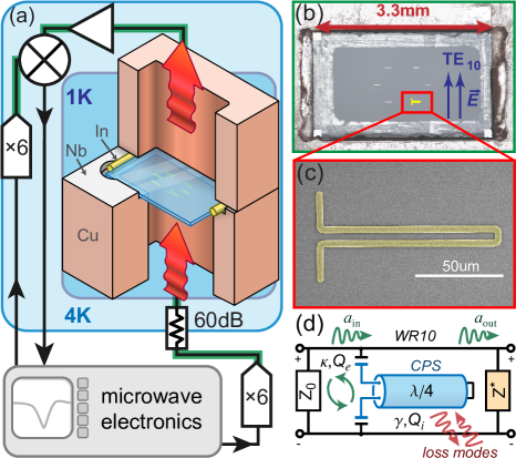
We investigate properties of millimeter-wave high KI resonators in the quantum regime at temperatures of K in a Helium-4 adsorption refrigerator. Using a frequency multiplier, cryogenic mixer and low noise amplifier, we measure the complex transmission response as shown in Fig. 1(a). Input attenuation reduces thermal noise reaching the sample, enabling transmission measurements in the single photon limit set by the thermal background. Rectangular waveguides couple the signal in and out of a m deep slot, the dimensions of which are carefully selected to shift spurious lossy resonances out of the W-band. To reduce potential conductivity losses, the waveguide and slot are coated with nm of evaporated Niobium. Below K this helps shield the sample from stray magnetic fields, however devices with higher are not shielded from magnetic fields while cooling through their superconducting transition. We use indium to mount a chip patterned with 6 resonators in the slot, as shown in Fig. 1(b). Devices are patterned on m thick sapphire which has low dielectric loss, and minimizes spurious substrate resonances in the frequency band of interest. The planar resonator geometry shown in Fig. 1(c) consists of a shorted quarter wave section of a balanced mode coplanar stripline waveguide (CPS), which couples directly to the TE10 waveguide through dipole radiation, which we enhance with dipole antennas. We find that this design is well described by the analytic model presented in Ref. Yoshida et al. (1992) which takes into account the thin film linear kinetic inductance. For very thin or narrow wire widths, the total inductance is dominantly kinetic, making the resonators extremely sensitive to superconducting film properties.
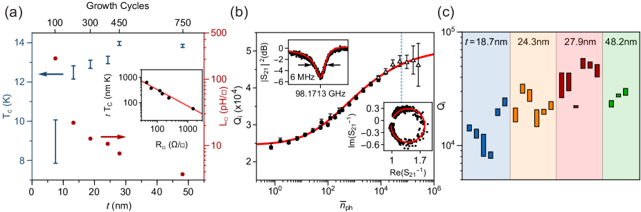
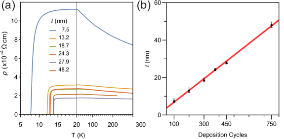
In order to understand the quality of the NbN films grown by ALD and accurately predict resonant frequencies, we characterize material properties with DC electrical measurements. All devices in this work are deposited on sapphire with a process based on Ref. Sowa et al. (2017), and etched with a fluorine based inductively coupled plasma. We measure resistivity at ambient magnetic fields as a function of temperature, which we use to extract for a range of film thicknesses [See Fig. 2(a)]. The inset also shows that our films follow a universal relation observed for thin superconducting films Ivry et al. (2014) linking , film thickness , and sheet resistance : we find that our results are similar to NbN deposited with other methods Beebe et al. (2016); Ivry et al. (2014). For thicker films, appears to saturate at -K which is comparable to other materials studies Sowa et al. (2017); Kamlapure et al. (2010); Ivry et al. (2014), while decreasing to K for the thinnest film (t=nm), which can be attributed to disorder enhanced Coulomb repulsions Skvortsov and Feigel’man (2005); Driessen et al. (2012). We also find that the superconducting transition width increases significantly for the thinner films, which can in turn be attributed to disorder broadened density of states Driessen et al. (2012) or reduced vortex-antivortex pairing energies at the transition Niepce et al. (2019); Mooij (1984).
From the resistivity and critical temperature we determine the sheet inductance where the normal sheet resistance is taken as the maximum value of normal resistivity , occurring just above , and is the superconducting energy gap predicted by BCS theory for NbN Niepce et al. (2019); Kamlapure et al. (2010). We observe a monotonic increase in for thinner films, achieving a maximum pH/, comparable to similar high KI films Shearrow et al. (2018); Mondal et al. (2011).
By characterizing complex transmission spectra of resonators fabricated on a range of film thicknesses, we explore loss mechanisms at millimeter-wave frequencies. The sheet inductance, thickness, and measured for a given film are used to adjust the resonator design length. This spreads resonances out in frequency from GHz to GHz, while varying antenna lengths allows us to adjust coupling strengths. A typical normalized transmission spectrum taken at single photon occupation powers () is shown in the inset of Fig. 2(b). On resonance, we observe a dip in magnitude, which at low powers is described well by Khalil et al. (2012):
| (1) |
where Khalil et al. (2012) and the coupling quality factor has undergone a complex rotation due to an impedance mismatch Khalil et al. (2012); Megrant et al. (2012), likely induced by the sapphire chip and slot altering waveguide geometry. We find that at high powers, begins to saturate, typically for [Fig. 2(b)]. This behavior is well described by a power dependent saturation mechanism Sage et al. (2011); Wang et al. (2009), likely originating from two-level systems in the slow growing amorphous surface oxide layer Medeiros et al. (2019). For some samples, due to relatively low bifurcation powers we do not observe high power saturation.
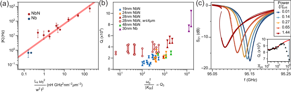
To study the effect of film thickness on , we repeat the measurements summarized in Fig. 2(b) for devices varying in thickness from 19.5 nm to 48.8 nm, and show the results in Fig. 2(c), where we plot the low and high power saturation values of for devices from six separate chips grouped by film thickness. For films thicker than 20nm, we consistently find , all of which show power dependence to varying extents. We find a weak correlation of with film thickness, which could be explained by several additional potential sources of loss. Thinner films exhibiting higher disorder have also been connected with a nonlinear resistance associated with kinetic inductance Yurke and Buks (2006). Additionally, since the devices are not shielded from ambient magnetic fields at the superconducting transition, resulting vortices trapped in the thin films may lead to additional dissipation Nsanzineza (2016); Kitaygorsky et al. (2007); Mooij (1984); Niepce et al. (2019) dependent on film thickness. Resonances patterned from thinner films proved experimentally difficult to distinguish from background fluctuations, possibly indicating low values of or frequencies shifted out of the measurement bandwidth.
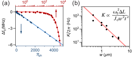
A key aspect of high KI resonators is their fourth-order nonlinearity: an important component for realizing quantum devices, and similar to the nonlinearity term found in Josephson junctions for low powers. Nonlinear kinetic inductance takes the general form , where is the linear kinetic inductance, the nonlinear kinetic inductance, and the critical current which sets the nonlinearity scale Yurke and Buks (2006); Kher (2017). This adds nonlinear terms of the form to the Hamiltonian, with , shifting the fundamental frequency by the self-Kerr constant (or anharmonicity) for each photon added. To characterize the strength of the resonator nonlinearity, we measure the resonance frequency shift 111The frequency corresponding to maximum photon occupation, or the point diametrically opposite as a function of photon number Maleeva et al. (2018). A linear fit for a resonator (nm, m) yielding kHz is shown in Fig. 3(a). By writing the self-Kerr coefficient in terms of a current density , we find that scales as , which we observe in 3(b). These results are comparable to self-Kerr strengths of granular aluminum nanowires Maleeva et al. (2018) or weakly nonlinear Josephson junctions Eichler and Wallraff (2014). Despite careful calibration of input powers supplied to the device, we note that minute variations in received power arising from shifting attenuation at cryogenic temperatures limit best estimates of photon number to within a factor of 10.
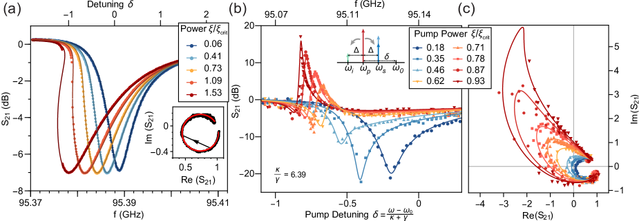
A hallmark of Kerr nonlinearity is the distortion of the transmission line-shape in frequency space at high powers, ultimately leading to a multi-valued response above the bifurcation power. Re-writing and , the steady-state nonlinear response takes the form derived from Refs. Yurke and Buks (2006); Swenson et al. (2013) (See Appendix A):
| (2) |
where the frequency detuning is written in reduced form , and is a function of frequency and reduced circulating power . We plot steady-state transmission data taken near the bifurcation power in Fig. 4(a) along with fits to Eq. 2, with system parameters , and constrained to low power values, and find the model in good agreement with measurements.
We further explore nonlinear dynamics by stimulating degenerate four-wave mixing with the addition of a continuous wave classical pump (see supplement Fig. S3). When a high power pump tone is on resonance with the down-shifted resonance frequency, and a low power signal is at a frequency detuning from the pump, we expect to observe the net conversion of two pump photons into a signal photon and an idler photon at their sum-average frequency [Fig. 4(b) inset]. This effect is most pronounced when all frequencies are within the resonant bandwidth, and the pump power approaches the bifurcation point , but is limited by the loss fraction . We measure the pump-signal conversion efficiency of a high-bandwidth, high- device in the propagation direction as a function of reduced pump frequency for increasing pump powers , and a fixed signal power corresponding to in Fig. 4(b-c). We find that this behavior is accurately captured with a model based on Refs. Eichler and Wallraff (2014); Yurke and Buks (2006) (see Appendix A), and overlay the results. For increasing pump powers, we observe smooth parametric deformation from the single tone response in the complex plane. For higher powers, we observe increasing gain with decreasing linewidth similar to Refs. Eichler and Wallraff (2014); Tholén et al. (2007), up to a maximum measured forward efficiency of +dB. The slight curvature in the complex plane is a result of the finite pump-signal detuning .
The demonstration of degenerate four-wave mixing realizes an important milestone for the development of quantum devices at millimeter-wave frequencies and temperatures above K. For NbN films thicker than nm, we measured millimeter-wave resonators with internal quality factors exceeding at single photon powers, and by reducing wire width to nm achieved self-Kerr nonlinearities up to kHz for linewidths ranging from -MHz. With some modification the devices in this work could easily be redesigned as parametric amplifiers, which at microwave frequencies have been shown to achieve near quantum-limited noise figures and quadrature squeezing Tholén et al. (2007); Eom et al. (2012); Tholén et al. (2007); Yurke (1987); Movshovich et al. (1990). While insufficient for implementing a millimeter-wave artificial atom, the Kerr nonlinearity we measure arising from high KI thin films can further be used for superinductors Bell et al. (2012); Niepce et al. (2019), photon frequency conversion Pechal and Safavi-Naeini (2017), parametric mode cooling Khan et al. (2015); Zhang et al. (2017), phase slip junctions Mooij and Nazarov (2006); Astafiev et al. (2012), and mode squeezing Tholén et al. (2007) realized at millimeter-wave frequencies. This opens the door to a new generation of high-frequency quantum experiments at temperatures above K.
Acknowledgements.
The authors would like to thank P. Duda, P. S. Barry, and E. Shirokoff for assistance developing deposition recipes, as well as M. Wesson and C. Sheagren for supporting film characterization. We acknowledge useful discussions with S. J. Whiteley, and also thank J. Jureller for assistance with MRSEC facilities. This work was supported by the Army Research Office under Grant No. W911NF-17-C-0024. This work was partially supported by the University of Chicago Materials Research Science and Engineering Center, which is funded by the National Science Foundation under award number DMR-1420709. This work was partially supported by the National Science Foundation Graduate Research Fellowship under Grant No. DGE-1746045. Devices were fabricated in the Pritzker Nanofabrication Facility at the University of Chicago, which receives support from Soft and Hybrid Nanotechnology Experimental (SHyNE) Resource (NSF ECCS-1542205), a node of the National Science Foundation’s National Nanotechnology Coordinated Infrastructure.References
- Devoret and Schoelkopf (2013) M. H. Devoret and R. J. Schoelkopf, Science 339, 1169 (2013).
- Braginski (2019) A. I. Braginski, Journal of Superconductivity and Novel Magnetism 32, 23 (2019).
- Xiang et al. (2013) Z.-L. Xiang, S. Ashhab, J. You, and F. Nori, Reviews of Modern Physics 85, 623 (2013).
- Morton and Lovett (2011) J. J. Morton and B. W. Lovett, Annu. Rev. Condens. Matter Phys. 2, 189 (2011).
- Vasilyev et al. (2004) S. Vasilyev, J. Järvinen, E. Tjukanoff, A. Kharitonov, and S. Jaakkola, Review of scientific instruments 75, 94 (2004).
- Aslam et al. (2015) N. Aslam, M. Pfender, R. Stöhr, P. Neumann, M. Scheffler, H. Sumiya, H. Abe, S. Onoda, T. Ohshima, J. Isoya, et al., Review of Scientific Instruments 86, 064704 (2015).
- Raimond et al. (2001) J.-M. Raimond, M. Brune, and S. Haroche, Reviews of Modern Physics 73, 565 (2001).
- Pechal and Safavi-Naeini (2017) M. Pechal and A. H. Safavi-Naeini, Physical Review A 96, 042305 (2017).
- Tucker and Feldman (1985) J. R. Tucker and M. J. Feldman, Reviews of Modern Physics 57, 1055 (1985).
- Niu et al. (2015) Y. Niu, Y. Li, D. Jin, L. Su, and A. V. Vasilakos, Wireless networks 21, 2657 (2015).
- Bozzi et al. (2011) M. Bozzi, A. Georgiadis, and K. Wu, IET Microwaves, Antennas & Propagation 5, 909 (2011).
- Chang et al. (2014) C. Chang, P. Ade, Z. Ahmed, S. Allen, K. Arnold, J. Austermann, A. Bender, L. Bleem, B. Benson, J. Carlstrom, et al., IEEE Transactions on Applied Superconductivity 25, 1 (2014).
- Brown et al. (2016) A. D. Brown, E. M. Barrentine, S. H. Moseley, O. Noroozian, and T. Stevenson, IEEE Transactions on Applied Superconductivity 27, 1 (2016).
- Zhang et al. (2012) C. Zhang, J. Wu, B. Jin, Z. Ji, L. Kang, W. Xu, J. Chen, M. Tonouchi, and P. Wu, Optics express 20, 42 (2012).
- Hanham and Ridler (2003) W. J. O. S. M. Hanham and N. M. Ridler, Nature 425, 944 (2003).
- Kuhr et al. (2007) S. Kuhr, S. Gleyzes, C. Guerlin, J. Bernu, U. B. Hoff, S. Deléglise, S. Osnaghi, M. Brune, J.-M. Raimond, S. Haroche, et al., Applied Physics Letters 90, 164101 (2007).
- Shirokoff et al. (2012) E. Shirokoff, P. S. Barry, C. M. Bradford, G. Chattopadhyay, P. Day, S. Doyle, S. Hailey-Dunsheath, M. I. Hollister, A. Kovács, C. McKenney, et al., in Millimeter, Submillimeter, and Far-Infrared Detectors and Instrumentation for Astronomy VI, Vol. 8452 (International Society for Optics and Photonics, 2012) p. 84520R.
- Endo et al. (2013) A. Endo, C. Sfiligoj, S. Yates, J. Baselmans, D. Thoen, S. Javadzadeh, P. Van der Werf, A. Baryshev, and T. Klapwijk, Applied Physics Letters 103, 032601 (2013).
- Gao et al. (2009) J. Gao, A. Vayonakis, O. Noroozian, J. Zmuidzinas, P. K. Day, and H. G. Leduc, in AIP Conference Proceedings, Vol. 1185 (AIP, 2009) pp. 164–167.
- Kongpop et al. (2016) U. Kongpop, A. D. Brown, S. H. Moseley, O. Noroozian, E. J. Wollack, et al., IEEE Transactions on Applied Superconductivity 27, 1 (2016).
- Kerr et al. (2013) A. R. Kerr, S.-K. Pan, S. M. Claude, P. Dindo, A. W. Lichtenberger, and E. F. Lauria, in 2013 IEEE MTT-S International Microwave Symposium Digest (MTT) (IEEE, 2013) pp. 1–4.
- Mears et al. (1990) C. Mears, Q. Hu, P. Richards, A. Worsham, D. Prober, and A. Räisänen, Applied physics letters 57, 2487 (1990).
- Grimm et al. (2017) A. Grimm, S. Jebari, D. Hazra, F. Blanchet, F. Gustavo, J. Thomassin, and M. Hofheinz, Superconductor Science and Technology 30, 105002 (2017).
- Olaya et al. (2019) D. Olaya, M. Castellanos-Beltran, J. F. Pulecio, J. Biesecker, S. Khadem, T. Lewitt, P. Hopkins, P. Dresselhaus, and S. Benz, IEEE Transactions on Applied Superconductivity (2019).
- Shearrow et al. (2018) A. Shearrow, G. Koolstra, S. J. Whiteley, N. Earnest, P. S. Barry, F. J. Heremans, D. D. Awschalom, E. Shirokoff, and D. I. Schuster, Applied Physics Letters 113, 212601 (2018).
- Samkharadze et al. (2016) N. Samkharadze, A. Bruno, P. Scarlino, G. Zheng, D. DiVincenzo, L. DiCarlo, and L. Vandersypen, Physical Review Applied 5, 044004 (2016).
- Hailey-Dunsheath et al. (2014) S. Hailey-Dunsheath, P. Barry, C. Bradford, G. Chattopadhyay, P. Day, S. Doyle, M. Hollister, A. Kovacs, H. LeDuc, N. Llombart, et al., Journal of Low Temperature Physics 176, 841 (2014).
- Noroozian et al. (2015) O. Noroozian, E. Barrentine, A. Brown, G. Cataldo, N. Ehsan, W.-T. Hsieh, T. Stevenson, K. U-yen, E. Wollack, and S. H. Moseley, in 26TH International Symposium on Space Terahertz Technology (2015).
- Ivry et al. (2014) Y. Ivry, C.-S. Kim, A. E. Dane, D. De Fazio, A. N. McCaughan, K. A. Sunter, Q. Zhao, and K. K. Berggren, Physical Review B 90, 214515 (2014).
- Kamlapure et al. (2010) A. Kamlapure, M. Mondal, M. Chand, A. Mishra, J. Jesudasan, V. Bagwe, L. Benfatto, V. Tripathi, and P. Raychaudhuri, Applied Physics Letters 96, 072509 (2010).
- Beebe et al. (2016) M. R. Beebe, D. B. Beringer, M. C. Burton, K. Yang, and R. A. Lukaszew, Journal of Vacuum Science & Technology A: Vacuum, Surfaces, and Films 34, 021510 (2016).
- Sowa et al. (2017) M. J. Sowa, Y. Yemane, J. Zhang, J. C. Palmstrom, L. Ju, N. C. Strandwitz, F. B. Prinz, and J. Provine, Journal of Vacuum Science & Technology A: Vacuum, Surfaces, and Films 35, 01B143 (2017).
- Niepce et al. (2019) D. Niepce, J. Burnett, and J. Bylander, Physical Review Applied 11, 044014 (2019).
- Yoshida et al. (1992) K. Yoshida, M. S. Hossain, T. Kisu, K. Enpuku, and K. Yamafuji, Japanese journal of applied physics 31, 3844 (1992).
- Skvortsov and Feigel’man (2005) M. Skvortsov and M. Feigel’man, Physical review letters 95, 057002 (2005).
- Driessen et al. (2012) E. Driessen, P. Coumou, R. Tromp, P. De Visser, and T. Klapwijk, Physical review letters 109, 107003 (2012).
- Mooij (1984) J. Mooij, in Nato Asi Series (Plenum Press New York, 1984) p. 325.
- Mondal et al. (2011) M. Mondal, A. Kamlapure, M. Chand, G. Saraswat, S. Kumar, J. Jesudasan, L. Benfatto, V. Tripathi, and P. Raychaudhuri, Physical review letters 106, 047001 (2011).
- Khalil et al. (2012) M. Khalil, M. Stoutimore, F. Wellstood, and K. Osborn, Journal of Applied Physics 111, 054510 (2012).
- Megrant et al. (2012) A. Megrant, C. Neill, R. Barends, B. Chiaro, Y. Chen, L. Feigl, J. Kelly, E. Lucero, M. Mariantoni, P. J. O’Malley, et al., Applied Physics Letters 100, 113510 (2012).
- Sage et al. (2011) J. M. Sage, V. Bolkhovsky, W. D. Oliver, B. Turek, and P. B. Welander, Journal of Applied Physics 109, 063915 (2011).
- Wang et al. (2009) H. Wang, M. Hofheinz, J. Wenner, M. Ansmann, R. Bialczak, M. Lenander, E. Lucero, M. Neeley, A. O’Connell, D. Sank, et al., Applied Physics Letters 95, 233508 (2009).
- Medeiros et al. (2019) O. Medeiros, M. Colangelo, I. Charaev, and K. K. Berggren, Journal of Vacuum Science & Technology A: Vacuum, Surfaces, and Films 37, 041501 (2019).
- Yurke and Buks (2006) B. Yurke and E. Buks, Journal of lightwave technology 24, 5054 (2006).
- Nsanzineza (2016) I. Nsanzineza, Vortices and Quasiparticles in Superconducting Microwave Resonators, Ph.D. thesis, Syracuse University (2016).
- Kitaygorsky et al. (2007) J. Kitaygorsky, I. Komissarov, A. Jukna, D. Pan, O. Minaeva, N. Kaurova, A. Divochiy, A. Korneev, M. Tarkhov, B. Voronov, et al., IEEE Transactions on Applied Superconductivity 17, 275 (2007).
- Kher (2017) A. S. Kher, Superconducting nonlinear kinetic inductance devices, Ph.D. thesis, California Institute of Technology (2017).
- Note (1) The frequency corresponding to maximum photon occupation, or the point diametrically opposite .
- Maleeva et al. (2018) N. Maleeva, L. Grünhaupt, T. Klein, F. Levy-Bertrand, O. Dupre, M. Calvo, F. Valenti, P. Winkel, F. Friedrich, W. Wernsdorfer, et al., Nature communications 9, 3889 (2018).
- Eichler and Wallraff (2014) C. Eichler and A. Wallraff, EPJ Quantum Technology 1, 2 (2014).
- Swenson et al. (2013) L. Swenson, P. Day, B. Eom, H. Leduc, N. Llombart, C. McKenney, O. Noroozian, and J. Zmuidzinas, Journal of Applied Physics 113, 104501 (2013).
- Tholén et al. (2007) E. A. Tholén, A. Ergül, E. M. Doherty, F. M. Weber, F. Grégis, and D. B. Haviland, Applied physics letters 90, 253509 (2007).
- Eom et al. (2012) B. H. Eom, P. K. Day, H. G. LeDuc, and J. Zmuidzinas, Nature Physics 8, 623 (2012).
- Yurke (1987) B. Yurke, JOSA B 4, 1551 (1987).
- Movshovich et al. (1990) R. Movshovich, B. Yurke, P. Kaminsky, A. Smith, A. Silver, R. Simon, and M. Schneider, Physical review letters 65, 1419 (1990).
- Bell et al. (2012) M. Bell, I. Sadovskyy, L. Ioffe, A. Y. Kitaev, and M. Gershenson, Physical review letters 109, 137003 (2012).
- Khan et al. (2015) R. Khan, F. Massel, and T. Heikkilä, Physical Review A 91, 043822 (2015).
- Zhang et al. (2017) J.-S. Zhang, W. Zeng, and A.-X. Chen, Quantum Information Processing 16, 163 (2017).
- Mooij and Nazarov (2006) J. Mooij and Y. V. Nazarov, Nature Physics 2, 169 (2006).
- Astafiev et al. (2012) O. Astafiev, L. Ioffe, S. Kafanov, Y. A. Pashkin, K. Y. Arutyunov, D. Shahar, O. Cohen, and J. Tsai, Nature 484, 355 (2012).
- Mazin (2005) B. A. Mazin, Microwave kinetic inductance detectors, Ph.D. thesis, California Institute of Technology (2005).
- Gao (2008) J. Gao, The physics of superconducting microwave resonators, Ph.D. thesis, California Institute of Technology (2008).
- Walls and Milburn (2007) D. F. Walls and G. J. Milburn, Quantum optics (Springer Science & Business Media, 2007).
- Pozar (2009) D. M. Pozar, Microwave engineering (John Wiley & Sons, 2009).
- Ridolfo et al. (2012) A. Ridolfo, M. Leib, S. Savasta, and M. J. Hartmann, Physical review letters 109, 193602 (2012).
- Lock et al. (2019) E. H. Lock, P. Xu, T. Kohler, L. Camacho, J. Prestigiacomo, Y. J. Rosen, and K. D. Osborn, IEEE Transactions on Applied Superconductivity 29, 1 (2019).
- Reagor (2016) M. J. Reagor, Superconducting Cavities for Circuit Quantum Electrodynamics, Ph.D. thesis, Yale University (2016).
- Tinkham (2004) M. Tinkham, Introduction to superconductivity (Courier Corporation, 2004).
- Mattis and Bardeen (1958) D. Mattis and J. Bardeen, Physical Review 111, 412 (1958).
- Hazra et al. (2018) D. Hazra, S. Jebari, R. Albert, F. Blanchet, A. Grimm, C. Chapelier, and M. Hofheinz, arXiv preprint arXiv:1806.03935 (2018).
- Hashemi et al. (2009) H. Hashemi, A. W. Rodriguez, J. Joannopoulos, M. Soljačić, and S. G. Johnson, Physical Review A 79, 013812 (2009).
- Talantsev and Tallon (2015) E. F. Talantsev and J. L. Tallon, Nature communications 6, 7820 (2015).
- Tsukamoto (2005) O. Tsukamoto, Superconductor Science and Technology 18, 596 (2005).
- Stan et al. (2004) G. Stan, S. B. Field, and J. M. Martinis, Physical review letters 92, 097003 (2004).
Appendix A Kerr nonlinear dynamics for a side-coupled resonator
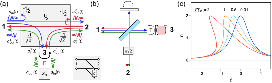
Here we outline a simple method inspired by Refs. Mazin (2005); Gao (2008) to decompose a side-coupled resonator into a linear network containing a one-sided cavity, which is very well understood in the language of input-output theory used in quantum optics Walls and Milburn (2007). This allows us to map well-modelled dynamics of a Kerr nonlinear cavity driven in reflection Yurke and Buks (2006); Eichler and Wallraff (2014) to a side-coupled resonator measured in transmission, obtaining results in agreement with Ref. Swenson et al. (2013), which uses a more direct approach.
Based on the circuit model in Fig. 1(d), and the argument that a symmetrically coupled resonator will radiate equally in both directions, we consider the the 3-port H-plane splitter. This lossless but unmatched network Pozar (2009) has symmetric ports 1-2 corresponding to the transmission line, and unmatched port 3 leading to the single-port coupled resonator as shown in Fig. S1(a) (This system can also be described by a network consisting of a 50-50 beamsplitter, perfect mirror, and phase shifter as shown in Fig. S1(b), which yields the same key results if we are careful to use correct boundary conditions). If we place a black-box element on port 3, we can describe it’s input and output fields in terms of the waveguide input and output fields:
| (A1) |
If we describe the black box with an arbitrary reflection term , the scattering matrix of the system reduces to:
| (A2) |
We can now verify that far off-resonance, for open circuit perfect reflection , we recover perfect transmission. With a map of waveguide inputs and outputs we replace the black box with Kerr nonlinear one-port coupled resonator, which has the steady state condition Walls and Milburn (2007); Eichler and Wallraff (2014):
| (A3) |
We have been careful to use the microwave convention for Fourier transforms, and corresponds to the average number of photons in the resonator. Multiplying by the complex conjugate, we obtain an equation governing the normalized number of photons in the resonator .
| (A4) |
Where similar to Ref. Eichler and Wallraff (2014), , and are defined as:
| (A5) | ||||
| (A6) | ||||
| (A7) |
We plot as a function of for varying drive strengths in Fig. S1(c), finding that reaches a maximum value of . At the critical value , Eq. A4 has 3 real solutions, leading to the onset of bifurcation. Based on the resonator boundary conditions Ridolfo et al. (2012) and Eq. A3, the reflection coefficient will be Walls and Milburn (2007); Yurke and Buks (2006); Eichler and Wallraff (2014)
| (A8) |
Far off resonance, an impedance mismatch on output port 2 results in nonzero reflection and transmission less than unity. To account for this while preserving the unitarity of the S matrix, we apply transformations of the form to each path of the 3 port network, yielding . Mapping Eq. A8 to the modified 3 port network, we obtain the result used in the main text, which in respective limits agrees with Refs. Khalil et al. (2012) and Swenson et al. (2013).
| (A9) |
At low powers (), Eq. A9 reduces to Eq. 1 in the main text.
We follow a similar approach to obtain expressions for parametric conversion gain using the derived input-output relations to map the key results from Ref. Eichler and Wallraff (2014) to the waveguide inputs and outputs. Using microwave conventions for Fourier transforms, the one-port gain of a signal detuned from the pump by is given by:
| (A10) |
With . Using the 3 port network transformations above yields the normalized forward (in direction of propagation) signal gain:
| (A11) |
Appendix B Device fabrication
All devices were fabricated on m thick C-plane (0001) Sapphire wafers with a diameter of mm. Wafers were cleaned with organic solvents (Toluene, Acetone, Methanol, Isopropanol, and DI water) in an ultrasonic bath to remove contamination, then were annealed at 1200∘C for 1.5 Hours. Prior to film deposition, wafers underwent a second clean with organic solvents (Toluene, Acetone, Methanol, Isopropanol, and DI water) in an unltrasonic bath, followed by 2 minute clean in 50∘C Nano-Strip™ etch, and a rinse with high purity DI water. The wafers then underwent a dehydration bake at 180∘C in atmosphere for 3 minutes.
Immediately afterwards, wafers were loaded into an Ultratech Fiji G2 plasma enhanced atomic layer deposition tool for metallization, where they first underwent a 1 hour bake at 300∘C under vacuum continuously purged with sccm of argon gas. Chamber walls matched the substrate temperature. The deposition parameters and machine configuration are adapted from Ref. Sowa et al. (2017). (-Butylimido)Tris(Diethylamido)-Niobium(V) (TBTDEN) was used as the niobium precursor, which was kept at 100∘C and delivered by a precursor Boost™ system, which introduces argon gas into the precursor cylinder to promote material transfer of the low vapor pressure precursor to the wafer Sowa et al. (2017). The deposition cycle consisted of three 0.5 second pulses of boosted TBTDEN followed by 40 seconds of W plasma consisting of sccm hydrogen and sccm nitrogen. A flow of sccm of nitrogen and sccm of argon was maintained throughout the deposition process. After deposition the wafer was allowed to passively cool to 250∘C under vacuum.
Following deposition, the wafers were cleaned with DI water in an ultrasonic bath to remove particulates, then underwent a dehydration bake at 180∘C in atmosphere for 3 minutes before spinning resist. For optical lithography, to avoid defocusing from wafer deformation, wafers were mounted to a Silicon handle wafer with AZ MiR 703 photoresist cured at 115∘C. Wafers were then coated with m of positive I-line photoresist AZ MiR 703, and exposed with a Heidleberg MLA150 Direct Writer. For electron Beam lithography, wafers were first coated with nm of negative resist ARN 7520, followed by nm of conductive resist ‘Elektra’ AR PC 5090, and then exposed with a Raith EBPG5000 Plus E-Beam Writer. The conductive coating was removed by a 60 second DI water quench. Both optical and E-Beam resists were baked at 110∘C to further harden the resist, and then developed for 60 seconds in AZ MIF 300, followed by a 60 second quench in DI water. We note that the rounded corners of our devices are by design to diffuse electric fields and reduce coupling to two level systems, and not defects induced by lithographic resolution.
The NbN films were etched in a Plasma-Therm inductively coupled plasma etcher. Etch chemistry, substrate etch depth and etch time have been shown to affect planar resonator quality factors Lock et al. (2019), in particular due to the formation of cross-linked polymers at the metal-resist interface after the bulk metal is etched away. For this reason we scale sample etch times to metal thickness, with a fixed over-etch time of 30 seconds to ensure complete metal removal. We use a Fluorine based ICP etch chemistry with a plasma consisting of sccm SF6, sccm CHF3, and sccm Ar. ICP and bias powers were kept at W, and the substrate was cooled to a temperature of 10∘C. Following etching, the resist was stripped in a combination of acetone and 80∘C Remover PG (N-Methyl-2-Pyrrolidone) which also serve to release the wafer from the Silicon carrier wafer. The wafers were then cleaned with organic solvents (Acetone, Isopropanol, and DI water), coated with a m protective layer of photoresist, and diced into mm chips. These were stripped of protective resist with 80∘C Remover PG, cleaned with organic solvents (Acetone, Isopropanol, and DI water), dried on an unpolished Sapphire carrier wafer in atmosphere at 80∘C, then mounted with Indium wire in the copper box described in the text.
Appendix C Film characterization
DC film characterization measurements were performed in a Quantum Design Physical Property Measurement System (PPMS) with a base temperature of K. Test structures consisting of a 1.5 mmm wire were patterned on mm chips going through the process described above along with device wafers, then wirebonded for four-wire measurements. Finished structures were kept in a low mTorr vacuum in an effort to minimize oxide growth prior to measurement, as we observed decreases up to K in critical temperatures for samples aged several days in atmosphere, likely a result of oxide growth Medeiros et al. (2019) reducing the superconducting film thickness.
After cooling the samples to K (K in the case of the nm film) in ambient magnetic fields, we verified that the residual resistance of the film dropped below the instrument noise floor of around . After thermalizing for one hour, the samples were warmed up to K at a rate of 0.K/min, then warmed to K at a rate of K/min. In Fig. S2(a) we plot measured resistivity as a function of temperature for the films in this study, which we use to extract , and calculate and for the films. Similar to previous studies Niepce et al. (2019), resistivity decreases with temperature above the superconducting transition, which is typical for strongly disordered materials Mondal et al. (2011); Niepce et al. (2019).
Appendix D Millimeter-Wave Measurement Setup and calibration
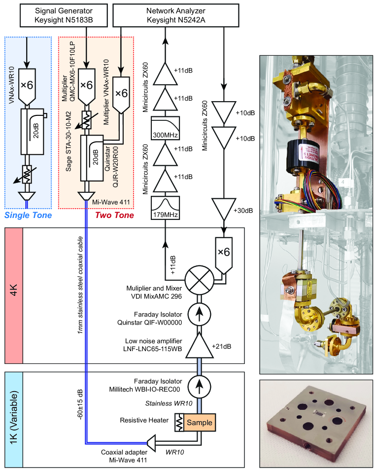
All millimeter-wave characterization was performed in a custom built 4He adsorption refrigerator, with a base temperature of K, and a cycle duration of 3 hours. We generate millimeter-wave signals (-GHz) at room temperature by sending microwave signals (-GHz) into a frequency multiplier. We convert the generated waveguide TE10 mode to a mm diameter stainless steel and beryllium copper coaxial cable, which carries the signal to the K stage of the fridge, thermalizing mechanically at each intermediate stage, then convert back to a WR-10 waveguide which leads to the device under test. The cables and waveguide-cable converters have a combined frequency-dependent loss ranging from dB to dB in the W-Band, which is dominated by the cable loss. We confirm the attenuation and incident device power at room temperature with a calibrated power meter (Agilent W8486A) and a referenced measurement with a VNAx805 receiver, however cryogenic shifts in cable transmission and minute shifts in waveguide alignment likely result in small variations in transmitted power. We are able to further confirm the applied power by measuring the lowest observed bifurcation point, and find that most bifurcation powers agree with predictions, yielding a maximum combined power uncertainty of approximately dBm, which sets the uncertainty in our photon number measurements.
The sample is isolated from both millimeter-wave and thermal radiation from the K plate with two stainless steel waveguides 2 inches long and a faraday isolator. Using a resistive heater and a standard curve Ruthenium oxide thermometer we can perform temperature sweeps on the sample without significantly affecting the fridge stage temperatures. A low-noise amplifier (K) amplifies the signal before passing through another faraday isolator, which further blocks any leaking signals. The signal then passes to a cryogenic mixer, which converts the signal to radio-wave (-MHz) which we filter, amplify and measure at room temperature with a network analyzer. We control signal power by varying input attenuation and multiplier input power, confirming with room temperature calibrations as described above. For two-tone measurements, we move the signal path to the dB port of the input directional coupler, and add an additional frequency multiplier fed by a reference-locked microwave signal generator. For single-tone measurements, the dB port is capped with a short to minimize incident stray radiation.
Appendix E BCS conductivity temperature dependence
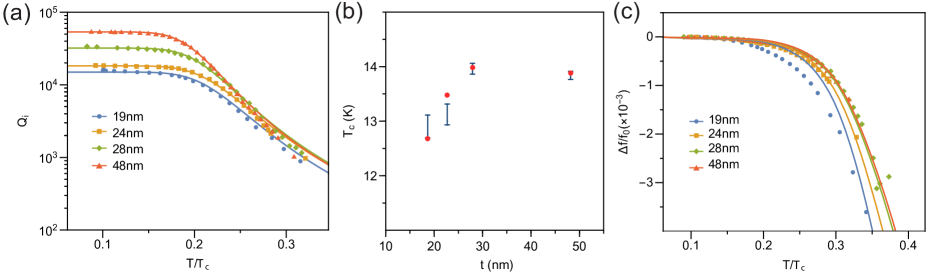
Due to the large kinetic inductance fraction , or magnetic field participation ratio of the thin film resonators, we expect higher sensitivity to conductor loss, which in turn is sensitive to temperature. In Fig. S4(a) we show the quality factor decrease as a function of temperature for resonators with four different thicknesses, with solid lines corresponding to a model of the form
| (E1) |
where is a temperature independent upper bound arising from other sources of loss, and the conduction loss is given by Reagor (2016):
| (E2) |
where and are the real and imaginary parts respectively of the complex surface impedance, calculated by numerically integrating the Mattis-Bardeen equations for and Reagor (2016); Tinkham (2004); Mattis and Bardeen (1958). We use and as fit parameters in the model. Below K ( ), saturates, which indicates that conduction loss does not limit for these devices. We note minor deviations from theory at higher temperatures, which may be a result of physical deviations from the standard curve calibrations used for the ruthenium oxide thermometer. Since these resonators were fabricated with measuring resonators at higher temperatures where is below proved experimentally challenging. In Fig. S4(b) we plot the fitted values against those obtained with DC measurements and find reasonable agreement for higher thickness films, however note that the uncertainty in temperature calibration combined with the relatively low saturation values result in fitted uncertainties around K.
Bardeen-Cooper-Schrieffer theory also predicts a shift in London length as a function of temperature, which in the dirty (high disorder) limit is given by Hazra et al. (2018); Tinkham (2004):
| (E3) |
We can measure this by tracking the resonant frequency shift. For sufficiently large kinetic inductance fractions, or , the kinetic inductance will dominate the total inductance, so the normalized frequency shift will be Hazra et al. (2018)
| (E4) |
In Fig. S4(c) shows the normalized frequency shift as a function of normalized temperature and predictions from Eq. E4 with parameters and taken from fits to above. Notably, we find significant deviation from the BCS theory for lower thicknesses, which has been previously observed for high-disorder films Shearrow et al. (2018); Beebe et al. (2016); Hazra et al. (2018).
Appendix F Controlling nonlinearity in the presence of additional losses
From Ref. Yurke and Buks (2006), we expect the self-Kerr nonlinearity originating from kinetic inductance of a resonator to be
| (F1) |
where in our case the nonlinear kinetic inductance is constant along the transmission line, so integrating over the fundamental mode profile yields a constant. We have also transformed the critical current into a critical current density , and used the assumption that the nonlinear kinetic inductance is proportional to the linear kinetic inductance Kher (2017); Swenson et al. (2013). Fig. S5(a) expands on Fig. 3(b), showing measured self-Kerr constants for all resonators in this study (grouped into points by film thickness and wire width) as a function the parameters in Eq. F1, with the solid line corresponding to a linear fit. We have also added data from identical resonators fabricated from 30nm electron-beam evaporated niobium to extend the parameter range. We find reasonable agreement with dependence on the parameters in Eq. F1, however note that the dependence is much less clear than that on wire width .
Nonlinear kinetic inductance is also associated with a nonlinear resistance of the same form . Based on Ref. Yurke and Buks (2006), and assuming the nonlinear resistance scales with kinetic inductance, losses associated with nonlinear resistance will be
| (F2) |
This indicates that upper bounds on nonlinear losses should scale as . In Fig. S5(b) we plot low and high power limits of devices in this study with the addition of nm Niobium devices described above, and find that for resonators with fixed wire widths m, there appears to be a potential correlation of with indicating nonlinear resistance may be a potential loss mechanism.
In our analysis, we have also neglected to take into account higher harmonics of the resonator, which will be coupled to the fundamental mode by cross-Kerr interactions , which for evenly spaced harmonics scale as Yurke and Buks (2006)
| (F3) |
Given the proportionality to , the correlation described above may also potentially be a result of cross-Kerr effects. For line-widths large enough to cover any deviations from evenly spaced higher harmonics, we anticipate see power dependent conversion processes: in particular for a Kerr nonlinear system with harmonics spaced at and , at powers approaching the critical power we would expect increased conversion efficiency from the fundamental to third harmonic Hashemi et al. (2009), which in our experiment would be observed as increased resonator loss at higher powers.
In Fig. S5(c) we show the atypical transmission spectra of a nm thick, m wide device with a particularly large line-width showing decreasing near the bifurcation power (above ), departing from the two-level system model described in the main text. This additional power-dependent loss may be the result of the nonlinear mechanisms described above, but may also be a result of circulating currents exceeding the thin film critical current density, which is lowered by the increased London lengths of the thinner films Talantsev and Tallon (2015); Tsukamoto (2005). However since the loss could also simply be a result of frequency dependent dissipation, the source remains unclear.
In Fig. S5(b), we also observe that resonators achieving higher nonlinearities by reducing wire width do not appear to be affected by the nonlinear loss rate described above. We also find that these devices do not showcase obvious signs of high power loss shown in Fig. S5(c). While this may be a result of the difference in fabrication methods (see Appendix B), the thinner wires may have higher vortex critical fields Stan et al. (2004) leading to reduced vortex formation, and thus lower loss associated with vortex dissipation. Additionally, the thinner wires at the shorted end of the quarter wave section of the resonator further shift the higher harmonics, potentially resulting in lower cross-Kerr conversion loss.