Strain engineering of oxide thin films for photocatalytic applications
Abstract
Photocatalytic materials are pivotal for the implementation of disruptive clean energy applications such as conversion of H2O and CO2 into fuels and chemicals driven by solar energy. However, efficient and cost-effective materials able to catalyze the chemical reactions of interest when exposed to visible light are scarce due to the stringent electronic conditions that they must satisfy. Chemical and nanostructuring approaches are capable of improving the catalytic performance of known photoactive compounds however the complexity of the synthesized nanomaterials and sophistication of the employed methods make systematic design of photocatalysts difficult. Here, we show by means of first-principles simulation methods that application of biaxial stress, , on semiconductor oxide thin films can modify their optoelectronic and catalytic properties in a significant and predictable manner. In particular, we show that upon moderate tensile strains CeO2 and TiO2 thin films become suitable materials for photocatalytic conversion of H2O into H2 and CO2 into CH4 under sunlight. The band gap shifts induced by are reproduced qualitatively by a simple analytical model that depends only on structural and dielectric susceptibility changes. Thus, epitaxial strain represents a promising route for methodical screening and rational design of photocatalytic materials.
I Introduction
The adverse effects of burning fossil fuels and the growing concentration of CO2 in the atmosphere are motivating intense research efforts towards large-scale production of clean fuels and conversion of carbon dioxide into useful chemicals. In this context, generation of H2 from water and reduction of CO2 into methane (CH4) and other valuable substances by using energy from sunlight represent two very promising sustainable approaches fajrina19 ; xie16 .
Sunlight-induced dissociation of H–O and C–O bonds in water environment involves the use of photocatalytic materials that should fulfill quite stringent electronic requirements. For instance, the band gap () of photocatalytic materials must be below eV in order to absorb solar radiation within the visible spectral range. At the same time, a semiconductor able to catalyze the synthesis of H2 in water or the reduction of CO2 into CH4 should possess a conduction-band edge higher in energy than the corresponding redox potential ( and eV, respectively, relative to the vacuum level) and the valence-band edge lower than the H2O oxidation potential ( eV) xie16 ; shenoy19 . Furthermore, active photocatalysis requires efficient separation of the photogenerated charge carriers (low exciton binding energy) and their rapid transportation to the reaction sites (long electron-hole recombination time) park16 .
Cerium and titanium dioxide, CeO2 and TiO2, are two extensively investigated catalyst materials that present high structural stability, commercial availability, and low toxicity. Examples of applications in which CeO2 and TiO2 are exploited include fuel and solar cells, water purification, corrosion-resistant coatings, therapeutic agents, and gas sensors, to cite just a few rahimi16 ; castano15 ; montini16 . Nevertheless, the band gap of both catalysts are larger than eV, which severely restricts their absorbance of sunlight (to only % of the solar irradiation that reaches the earth’s surface kowalsa08 ). Chemical and nanostructuring strategies have been employed successfully to reduce the band gaps of CeO2 and TiO2 and thus improve their photocatalytic activity under sunlight asahi01 ; mitsudome11 . Nevertheless, the usual complexity associated with the energy landscapes of nanomaterials and the required synthesis methods make it difficult to identify what key parameters improve photocatalytic efficiency irrespective of the material park16 . As a consequence, progress in “photocatalysis by design”, which is different from just ranking photocatalyst materials by their performance (“black box screening”), remains limited takanabe17 . In addition to such design constraints, precious co-catalysts like Pt and Au typically are employed for improving photocatalytic performance, which is not suitable for practical applications xie16 ; kowalsa08 .
In this article, we show by means of first-principles simulations based on density functional theory that biaxial strain, (which can be achieved in practice by growing thin films on substrates presenting a lattice parameter mismatch through, for example, pulsed laser deposition techniques hu18 ; heo17 ), can be exploited to tune the optoelectronic and photocatalytic properties of some binary oxides in a substantial and controlled manner. Specifically, we predict that under feasible tensile strains of and % gopal17 ; benson17 CeO2 and TiO2 become suitable materials for conversion of H2O into H2 and of CO2 into CH4 under sunlight. Such potential enhancements in photocatalytic activity result from sizeable band gap reductions (%) and correct positioning of the valence and conduction-band edges under . Meanwhile, the effects of epitaxial strain on the band gap of ZnO, another well-known semiconductor photocatalyst choi18 , are found to be only marginal (%). We present quantitative and physically intuitive arguments that explain the origins of such irregular -driven effects on in terms of dielectric susceptibility and metal-oxygen bond length changes.
It is worth noting that recent experimental and theoretical works have already proposed epitaxial strain as a means for tuning in some oxide materials such as TiO2 yin10 ; kelaidis18 , ZnO choi18 , SnO2 zhou14 , and CdO yan12 . However, a clear and general understanding of how biaxial strain affects the photocatalytic performance of binary oxides is still missing. For instance, the relative variations induced by tensile biaxial strain are negative in some materials (band gap decreases in TiO2 and SnO2 yin10 ; zhou14 ) whereas positive in others (band gap increases in ZnO choi18 ). Likewise, the changes driven by compressive biaxial strain are positive in some materials (TiO2 and SnO2 yin10 ; zhou14 ) whereas negative or almost null in others (ZnO choi18 and CdO yan12 ). These results indicate that the causes of -induced band gap shifts cannot be traced down uniquely to simple structural changes yin10 ; zhou14 ; wagner02 since those changes are quite monotonous under biaxial strain regardless of the material. Moreover, the influence of on the band alignments of binary oxides has been neglected in previous studies despite their potential impact on the photocatalytic activity. Hence, the present theoretical work identifies the key factors that drive -induced band gap changes and fills the existing knowledge gaps. The results presented next show that strain engineering, either used on its own or as a complement to other existing approaches, can be a powerful tool for rational design and systematic improvement of photocatalytic materials.
II First-principles computational methods
First-principles calculations based on density functional theory (DFT) cazorla15a ; cazorla12b ; cazorla17a are performed to simulate and analyze the influence of biaxial strain () on several representative binary oxide photocatalysts. We use the PBEsol functional pbesol as is implemented in the VASP software package vasp . A “Hubbard–” scheme hubbard with eV is employed for a better treatment of the localized Ce , Ti , and Zn electronic orbitals. We use the “projector augmented wave” method to represent the ionic cores paw by considering the following electrons as valence: Ce , , , and ; Gd , , and ; Ti , , , and ; Zn and ; and O and . Wave functions are represented in a plane-wave basis truncated at eV. For integrations within the Brillouin zone we employ Monkhorst-Pack k–point grids kpoint with a density equivalent to that of in the fluorite CeO2 unit cell. Strained-bulk geometry relaxations are performed with a conjugate-gradient algorithm that allows for volume variations while imposing the structural constraints defining thin films ( and ) cazorla15 ; cazorla17 ; cazorla17b ; cazorla18 . Periodic boundary conditions are applied along the three directions defined by the lattice vectors, so that possible surface effects are completely avoided in the simulations. The relaxations are halted when the forces acting on the atoms fall below eVÅ-1. By using these technical parameters we obtain zero-temperature energies that are converged to within meV per formula unit. Biaxial strain conditions are simulated at % intervals. In order to estimate accurate band gaps and band alignments, we employ the hybrid HSE06 exchange-correlation functional hse06 to perform single-point calculations on the equilibrium geometries determined at the PBEsol level shenoy19 . The generation of non-stoichiometric and Gd-doped fluorite CeO2 thin films are explained in the Supplementary Methods along with some details of their energy and structural properties.
To calculate accurate band alignments we follow the work done by Moses and co-workers on binary semiconductors moses11 . Briefly, both bulk and slab calculations are performed from which the alignment of the electrostatic potential within the semiconductor material can be obtained relative to the vacuum level. From the slab calculations, the difference between the average electrostatic potential within the semiconductor material and in vacuum is obtained. From the bulk calculations, the band structure shifts relative to the average electrostatic potential are determined. These calculations are performed at each point and involve the estimation of macroscopic and planar average potentials (Supplementary Methods). The planar potential is computed by averaging potential values within a well defined plane (for instance, perpendicular to the surface of the slab), and the macroscopic potential is obtained by taking averages of the planar potential over distances of one unit cell along the chosen direction resta88 ; cazorla12 . The slab systems should be thick enough to ensure that the electron density in the center of the slab is practically equal to that in the bulk material. We have found that – nm thick oxide slabs accompanied by similarly large portions of vacuum provide sufficiently well converged results for the electrostatic potentials. Further technical details of our band alignment calculations are provided in the Supplementary Methods.
III Results and Discussion
The changes induced by biaxial strain, , on the structural, electronic, and photocatalytic properties of CeO2, TiO2, and ZnO as calculated with first-principles methods based on density functional theory (DFT, Sec. II and Supplementary Methods) are presented first. Both compressive () and tensile () biaxial strains ranging from zero up to a maximum absolute value of % have been considered in the simulations. These values are comparable in magnitude to the ’s achieved experimentally in the same materials gopal17 ; benson17 ; choi18 . At the end of this section, we introduce a simple analytical model that depends only on structural and dielectric susceptibility changes and reproduces qualitatively, and helps in understanding, the general band gap trends induced by .
III.1 Fluorite CeO2 (111)
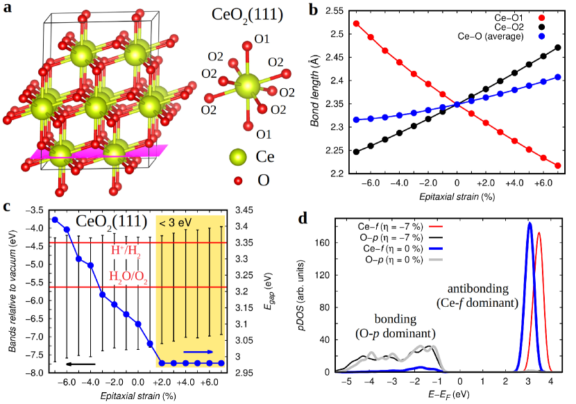
At room temperature, bulk ceria (CeO2) presents a cubic phase known as fluorite (space group ) in which the Ce ions form a face centered cubic sublattice and the oxygens a simple cubic. Ceria thin films commonly exhibit three high-symmetry orientations , , and . In this section, we consider the case; results for the geometry will be presented in the next section.
In the fluorite structure each Ce ion is surrounded by eight equidistant oxygens. Upon application of (111) biaxial strain, some crystal symmetries are broken (space group changes to ) and two characteristic metal-oxygen bond lengths emerge, Ce–O1 and Ce–O2, which are six- and two-fold degenerate, respectively (Fig.1a). The Ce–O1 bonds are oriented perpendicular to the (111) plane, in which the strain is applied, and thus under compressive (tensile) biaxial strain they are stretched (reduced). Conversely, the Ce–O2 bonds, which are mostly contained within the (111) plane, are shortened (stretched) under compressive (tensile) biaxial strain (Fig.1b). Due to the higher degeneracy of the Ce–O2 bonds, the average metal-oxygen neighbouring length decreases under compressive biaxial strain and increases under tensile (Fig.1b). For instance, at the maximum simulated compressive (tensile) biaxial strain the average Ce–O distance is reduced (elongated) by ()% of the unstrained value.
The sizable structural changes induced by suggest the possibility of finding similarly large variations in the band gap () of (111)–oriented CeO2 thin films yin10 ; zhou14 . In fact, as shown in Fig.1c, this turns out to be the case. Specifically, increases practically linearly under compressive biaxial strain, reaching a maximum value of eV at %. According to our DFT calculations the band gap of unstrained CeO2 is eV, which compares very well with the experimental value of eV goubin04 , hence a maximum relative increase of % is achieved. Under tensile biaxial strain, also varies significantly although not in a regular manner. The band gap first decreases to below eV at % but beyond that strain point its value remains practically constant (Fig.1c). As a result, a maximum -driven reduction of % is obtained. It is worth noting that the largest variation is achieved under compressive whereas the largest average Ce–O length change is achieved under tensile strain. This observation suggests that, at least for (111)–oriented CeO2 thin films, the band gap shifts induced by cannot be explained exclusively in terms of the accompanying structural changes.
Figure 1c also shows the band alignments of (111)–oriented CeO2 thin films, that is, the energy level of the valence-band (VB) and conduction-band (CB) edges as a function of . In the absence of any strain, our calculations predict a VB edge located at eV and CB at eV with respect to the vacuum level, which are in fairly good agreement with the available experimental data ( eV and eV wen18 ). For photocatalytic water-splitting purposes, the electronic band structure of unstrained CeO2 (111) presents two important limitations. First, the corresponding is too large for absorption of visible light, and second, the position of the VB (CB) edge is too far below (too close to) the water oxidation potential of eV (the proton reduction potential of eV) xie16 ; shenoy19 . Interestingly, biaxial strain can be used to partly overcome both of those limitations. Under tensile strain, the energy of the VB edge increases steadily and becomes equal to eV at %, eV closer to the water oxidation potential than for unstrained CeO2. At the same strain, the CB edge reaches a maximum value of eV and the band gap becomes smaller than eV. Thus, under sunlight can be absorbed more efficiently and the VB and CB edges are situated more appropriately for water splitting (that is, eV below and eV above the corresponding redox potentials). Meanwhile, under compressive strain the energy of the VB edge decreases steadily and the CB level remains more or less constant. As a consequence, the band gap of CeO2 (111) increases almost linearly with increasing strain magnitude in the region. We note that the band gap of unstrained bulk ceria is indirect and remains so in the investigated interval (Supplementary Figure 1).
The influence of biaxial strain on the VB and CB edges of CeO2 (111) (and thus on the band gap, defined as ) can be understood in terms of the concomitant electronic and structural changes. In bulk ceria, the top of the VB is mostly composed of oxygen orbitals that form a bonding state with Ce orbitals, while the bottom of the CB is mostly composed of cerium orbitals that form an antibonding state with O orbitals (Fig.1d). Compressive (tensile) strain reduces (increases) the average Ce–O bond length, which energetically favors (frustrates) the bonding state. Consequently, the energy of the VB edge decreases under and increases under . On the other hand, the bottom of the CB is found to be quite insensitive to compressive strains (Fig.1c). When the anion-cation bond lengths are reduced, the kinetic energy associated with the antibonding state typically increases (since it is proportional to , where represents the reciprocal lattice vector in the extended Brillouin zone) wei99 ; that increase in kinetic energy would bring the CB higher in energy. However, the – level repulsion appears to diminish slightly under compressive strain owing to the increased delocalization of the Ce orbitals (see density of states peaks above the Fermi energy level in Fig.1d, where the Ce states extend over a wider energy range for ). These two effects tend to oppose each other thus leaving the CB edge unaffected by compressive strain. Under tensile strain, the energy of the antibonding state eventually rises due to a significant increase in the localization of the Ce orbitals (Supplementary Figure 2) which enhances the – level repulsion and overcomes the accompanying decrease in kinetic energy.
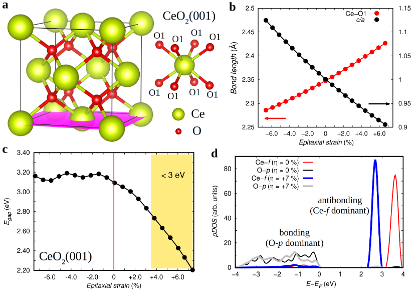
III.2 Fluorite CeO2 (001)
Upon application of (001) biaxial strain, the degeneracy of the eight equidistant oxygens surrounding each Ce ion (characteristic distance Ce–O1 in Fig. 2a) is not lifted, but the symmetry of the crystal changes from cubic to tetragonal (space group ) due to contraction or elongation of the out-of-plane axis relative to the two in-plane lattice vectors (Fig.2b). The changes driven by (001) strain on are noticeably different from those found in the (111) case (Figs.2c and 1c). In particular, the band gap now is hardly affected by compressive strain but is significantly reduced under tensile strain. For instance, at % the band gap is eV, % lower than the value obtained at equilibrium conditions; at %, is already smaller than eV. Plots of the electronic energy bands indicate that the band gap remains indirect regardless of (Supplementary Figure 3), as for the CeO2 (111) thin films.
The influence of on the band edges of (001)–oriented CeO2 thin films can also be rationalized in terms of the accompanying structural and electronic changes. In this case, we have not explicitly calculated the band alignments however, in analogy to the (111) case, we assume that the energy of the VB edge decreases under (increases under ) due to enhancement (frustration) of the – bonding interactions induced by shortening (elongation) of the Ce–O1 bonds. Based on this assumption and there being no effect of compressive strain on the band gap, it is expected that the energy of the CB edge decreases under compressive strain due to increased delocalization of the unoccupied Ce orbitals (Supplementary Figure 4), which weakens the – antibonding interactions and counteracts the concurrent increase in kinetic energy wei99 . Hence, both the VB and CB edges decrease under producing no net change in the band gap. Under tensile strain, however, it can be inferred from the decrease in the band gap that the bottom of the conduction band remains more or less constant with respect to the vacuum level, possibly due to a compensation effect between the increased localization of the Ce orbitals (see density of states peaks above the Fermi energy level in Fig.2d, where the Ce states extends over a narrower energy range for ), which tends to bring the CB higher in energy, and the reduction in kinetic energy, which tends to lower it.
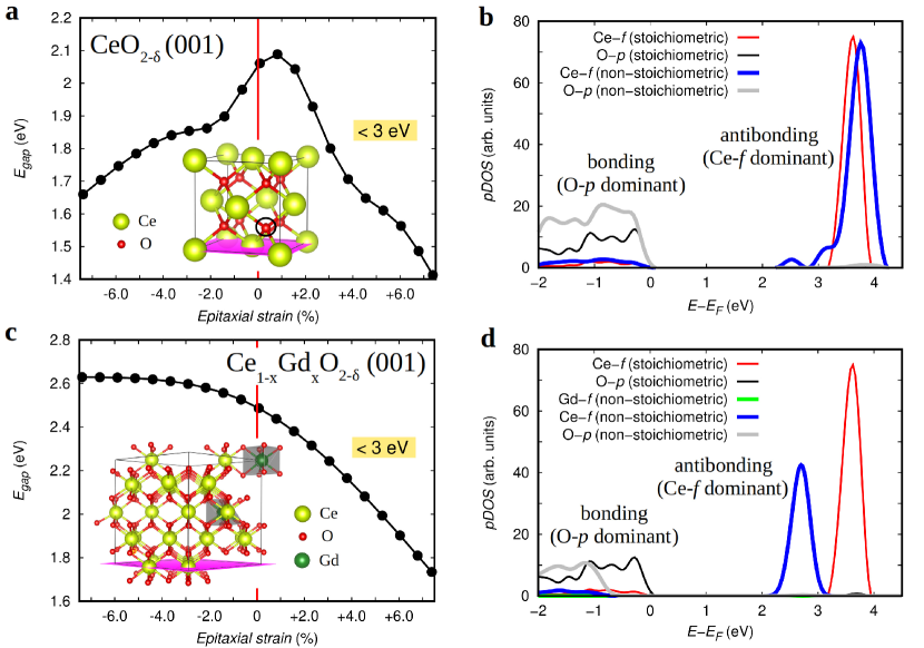
It has been demonstrated thus far that biaxial strain can have a significant impact on the optoelectronic properties of stoichiometric CeO2. It is reasonable to ask then whether similar control of functionality can be achieved in non-stoichiometric and metal-doped ceria thin films with , which can be prepared through advanced synthesis techniques mofarah19 ; korobko12 . The results shown in Fig.3 indicate that this is indeed the case. Our simulations of non-stoichiometric ceria, CeO2-δ, considering an arbitrary but representative of mofarah19 (Sec. II and Supplementary Methods), show that both positive and negative ’s can be used to reduce substantially (by % of the value obtained at zero strain, which is eV), with tensile strain being particularly effective (Fig.3a). Band gaps of and eV are obtained respectively at the highest compressive and tensile strain values considered in this study. These sizable reductions result from the combined action of oxygen vacancies, which are known to reduce the neighbouring Ce4+ ions and lower the CB edge due to the appearance of new unoccupied states (Fig.3b) mofarah19 , and biaxial strain.
Likewise, in Ce1-2xGd2xO2-x (001) thin films with an arbitrary but representative composition of korobko12 , our DFT simulations (Sec. II and Supplementary Methods) indicate that tensile strain is also capable of reducing considerably (Fig.3c). For instance, at % the band gap of Gd-doped ceria is eV, which is approximately % smaller than the value estimated at zero strain ( eV). In Gd-doped ceria, the presence of Gd3+ ions prevents the reduction of Ce4+ ions surrounding the oxygen vacancies (in contrast to what occurs in CeO2-δ). As a consequence, the relative variation induced by in Ce1-2xGd2xO2-x (001) is very similar to that found in the undoped stoichiometric system (Fig.2c). The high delocalization of the Ce orbitals forming the bottom of the CB in Ce1-2xGd2xO2-x (001) (Fig.3d), however, leads to a noticeable reduction in the band gap as compared to undoped CeO2 (001), which renders a practically constant difference of eV between the two systems across the entire range of values.
III.3 Anatase TiO2 (001)
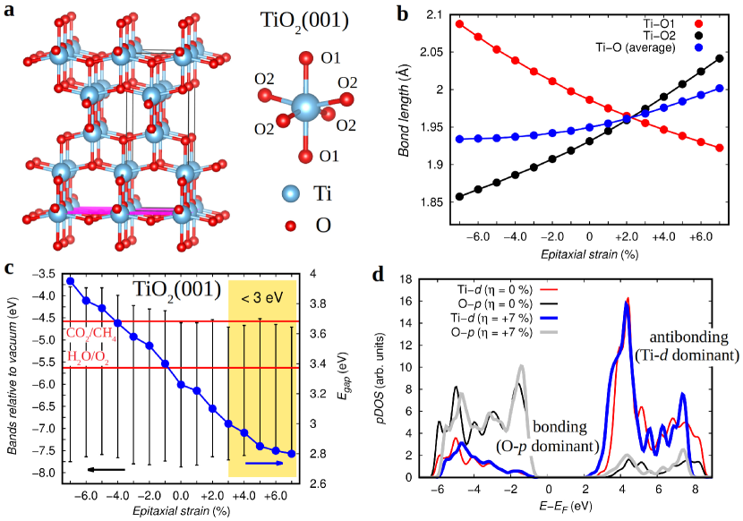
Bulk TiO2 is generally found in the rutile, anatase, or brookite phase. The rutile and anatase polymorphs find use in major industrial applications while brookite is of little technological relevance due to its difficult synthesis yamada12 . Rutile possesses tetragonal symmetry (space group ) and a band gap of eV, and is the energetically most favorable polymorph at room temperature. Anatase also presents tetragonal symmetry (space group ) and its band gap is eV yamada12 . Although the of anatase is larger than that of rutile, the former phase typically exhibits superior photocatalytic activity owing to better positioning of the band edges and longer electron-hole recombination times batzill11 ; choi94 . Hence it is of particular interest to investigate the influence of on the band gap and band alignments of anatase, to see whether it is possible to further improve the photocatalytic performance of TiO2.
In anatase TiO2, each Ti ion is surrounded by six neighbouring oxygens and forms two characteristic bonds with them, Ti–O1 and Ti–O2, which are respectively two- and four-fold degenerate (Fig.4a). When biaxially strained in the (001) plane, the Ti–O1 bonds, which are oriented out-of-plane, become elongated under compressive strain and shortened under tensile strain (Fig.4b). Conversely, the Ti–O2 bonds, which are oriented at only a small angle to the (001) plane, are reduced under and stretched under (Fig.4b). Consequently, as in most oxide semiconductors cazorla17 ; bousquet10 , the average metal-oxygen bond length decreases under compressive strain (by % of the equilibrium value at %) and increases under tensile strain (by % at %).
Concerning the electronic properties, at zero biaxial strain we estimate eV, which is in good agreement with the experimental value of eV yamada12 . Under compressive strain, the band gap increases almost linearly, achieving a maximum value of eV at % (Fig.4c). Under tensile strain, however, the band gap decreases steadily and becomes smaller than eV at %. A minimum band gap of eV is estimated at the largest tensile distortion considered in this study (Fig.4c). We note that remains indirect regardless of (Supplementary Figure 5).
Such a regular variation driven by biaxial strain across the entire range of strain values is in contrast to what was found for both the (111) and (001) orientations of CeO2, and can be explained in terms of the concurrent VB and CB edge shifts (Fig.4c). In bulk anatase, the top of the VB is principally composed of oxygen orbitals that form a bonding state with Ti orbitals while the bottom of the CB is mostly composed of Ti orbitals that form an antibonding state with O orbitals (Fig.4d). Compressive strain has little effect on the position of the VB edge, due to a compensation effect between enhancement of bonding interactions (which tends to lower the VB) and increase in kinetic energy (which tends to increase the VB), whereas tensile strain tends to bring it higher in energy, owing to frustration of the bonding state (which dominates over the decrease in kinetic energy). Meanwhile, the position of the CB edge moves significantly higher in energy under compressive strain, due to a dominant increase in the kinetic energy (since the localization of the unoccupied Ti orbitals appears to decrease slightly at , Supplementary Figure 6). Under tensile strain, the CB edge remains more or less constant owing to a small increase in the localization of the unoccupied Ti orbitals at (Fig.4d) that is counterbalanced by a decrease in the kinetic energy. We note that, in analogy to CeO2 thim films, the shifts induced by do not appear to be directly or exclusively correlated with the accompanying structural changes (i.e., the band gap variation is almost linear across the entire range of values, Fig.4c, whereas the structural fluctuations are most prominent under tensile strain, Fig.4b).
The band alignments in anatase TiO2 (001) are greatly affected by biaxial strain (Fig.4c). In the absence of planar stress, our calculations render a VB edge at eV and CB at eV relative to the vacuum level, which are in reasonable agreement with the available experimental data ( eV and eV batzill11 ). Under tensile strains of %, the band gap becomes smaller than eV, the corresponding VB edge gets closer to the H2O oxidation potential (for instance, at %, is eV), and the CB edge remains more or less constant around the value eV. At these biaxial strain conditions, the energy of the CB edge is around the reduction potential of CO2 (Fig.4c), hence tensilely strained anatase is predicted to be a suitable photocatalyst for driving the conversion of carbon dioxide into methane (CH4) in aqueous environment under visible light xie16 . Given the proximity of the CO2 and water reduction potentials, it is likely that biaxially strained anatase TiO2 () is also a suitable material for driving the production of hydrogen fuel from H2O under visible light.
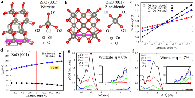
III.4 Zinc-blende and wurtzite ZnO (001)
ZnO thin films are used in a wide variety of optoelectronic applications due to the relative abundance of their elements and direct band gap of eV ozgur05 . The two common ZnO polymorphs are wurtzite (hexagonal symmetry, space group ) and zinc-blende (cubic symmetry, space group ), which are shown in Figs.5a-b. In wurtzite ZnO, each metal ion is coordinated to four neighboring oxygens and forms two characteristic metal-oxygen bond lengths, Zn–O1 and Zn–O2 (Fig.5a), which are single and three-fold degenerate, respectively. The evolution of the Zn–O1 and Zn–O2 distances as induced by in the (001) plane are shown in Fig.5c. The Zn–O1 bond length is oriented out-of-plane and displays an anomalous behavior in the sense that it contracts under compressive biaxial strain and expands under tensile biaxial strain. Such an anomalous behavior, which is not observed in the Zn–O2 case (Fig.5c), probably is related to the negative thermal expansion observed in bulk ZnO wang13 . On average, however, the mechanical behavior of wurtzite ZnO thin films is normal, namely, volume contraction at and volume expansion at relative to the unstrained reference system. Meanwhile, the zinc-blende structure, in which there is only one type of bond length, Zn–O1 (Fig.5b), presents a quite typical deformation behavior when biaxially strained in the (001) plane.
Figure 5d shows the band gaps of (001)–oriented ZnO thin films as a function of biaxial strain for the two crystal structures. In the absence of any strain, we estimate an of eV for the wurtzite phase and eV for the zinc-blende phase. These results, in contrast to the systems analyzed previously, are not in good agreement with the experimental value of eV choi18 . A possible explanation for such a large band gap discrepancy may be the very low density of electronic states found at the bottom of the CB (Fig.5e), which may complicate the estimation of both at the experimental and theoretical levels.
We find that the impact of on the band gap of ZnO thin films is practically negligible (at least in comparison to the CeO2 and TiO2 cases), which is consistent with previous experimental observations choi18 . For instance, according to our first-principles calculations, for the wurtzite phase increases by just % at % and decreases by % at %; in comparison, a reduction of % was obtained at % in experimental work choi18 . Meanwhile, the band gap for the zinc-blende phase is changed by even smaller amounts, with only a % reduction at % and a % increase at % (note the opposite sign in the strain-driven change as compared to the wurtzite case, Fig.5d). We note that the band gap of ZnO remains direct for all (Supplementary Figure 7).
The reason behind the marginal effects of biaxial strain on the of ZnO thin films seems to be related to the fact that the majority of electronic states forming both the top of the VB and the bottom of the CB are oxygen orbitals (Figs.5e-f and Supplementary Figure 8). As a consequence of such an electronic band-structure symmetry the VB and CB edges are shifted very similarly when the crystal is subjected to external stress, thus leaving practically invariant.
III.5 Explanation of the observed trends using a simple model
In previous sections we have demonstrated by means of computational first-principles methods that biaxial strain can be used to alter substantially the optoelectronic and photocatalytic properties of some binary oxide semiconductors. However, the influence of on the electronic band structure properties of binary oxide materials appears to be non-systematic and consequently difficult to predict. For instance, compressive biaxial strain hardly has any effect on the band gap of (001) CeO2 thin films whereas it induces a large increase in both (111) CeO2 and (001) TiO2 (Secs.III.1–III.3). On the other hand, the effects of on the structural properties of binary oxides (provided that are stable and do not undergo phase transitions) are quite regular and relatively easy to foresee. Essentially, the metal-oxygen bond lengths for all the analyzed oxides are stretched by an average value of % under moderate tensile biaxial strains and reduced by roughly the same amount under compressive biaxial strains. These outcomes suggest that the origins of the optoelectronic and photocatalytic variations induced by biaxial strain cannot be explained uniquely in terms of simple structural changes yin10 ; zhou14 ; wagner02 . In fact, a more sophisticated and general understanding of how photocatalytic activity can be tuned through is highly desirable for improving the design and computational screening of potential energy materials.
According to well-established theories omar75 , the band gap of a material is influenced by the first Fourier coefficient of the crystal field, which results from the superposition of atomic potentials within the solid. The crystal field essentially depends on the interatomic distances, dielectric screening (or, alternatively, quantity of charge in the atomic environment), and density of atoms in the solid sun01 . By shortening the atomic distances and/or weakening the dielectric screening, the crystal field is enhanced and as a result the band gap is widened. Conversely, by increasing the bond lengths and/or enhancing the dielectric screening the crystal field is depleted and the band gap is reduced. Therefore, there are two possible ways of modifying the crystal field along with the band gap in a structurally stable solid – changing its lattice parameters and/or its dielectric properties sun01 .
By combining deformation potential theory (, where represents mechanical stress) yin10 ; wei99 and the Kramers-Kroning relation (, where represents the dielectric susceptibility of the material) sun01 ; lu15 , we have deduced a simple analytical model that is able to describe qualitatively the band gap variations induced by biaxial strain on binary oxide semiconductors. Specifically, we express the -driven relative variations of the band gap as:
| (1) |
where the dependence of each term on biaxial strain is explicitly noted (for instance, “(0)” denotes unstrained), , represents the average metal-oxygen bond length, and the stress-strain relationship has been used (the minus sign accounts for the fact that negative biaxial strains correspond to positive stresses and vice versa). Our model treats the effects of structural and dielectric fluctuations on the band gap as independent quantities, that is, where and are the two functions specified above; because of this, the model cannot be quantitatively exact. Nevertheless, in spite of its limitations, this model provides a general and physically intuitive understanding of the results reported in the previous sections for binary oxides without the need to consider the details of the specific band structure of each material.
Table I shows the values obtained for biaxially strained CeO2, TiO2, and ZnO thin films at the largest ’s considered in this study using both DFT methods (exact) and the analytical model expressed in Eq.(1) (approximate). The corresponding and values are also reported in Table I. The dielectric susceptibility is calculated with the formula , where represents the ion-clamped dielectric constant of the material (estimated with perturbation DFT techniques) cazorla15 . In the case of CeO2 and TiO2 thin films Eq.(1) reproduces the relative band gap variations induced by biaxial strain correctly (albeit only at the qualitative level). For example, the analytical model predicts a reduction (increase) in under tensile (compressive) strain and the largest band gap variation is found for (001)–oriented CeO2 thin films at . On the other hand, the values estimated with Eq.(1) are systematically lower in magnitude than those calculated directly with DFT techniques by roughly a factor of . In the case of ZnO thin films, the analytical model consistently predicts band gap variations similar in magnitude to those obtained with DFT methods; however, the corresponding signs are reversed in most cases. This comparison indicates that the limitations of Eq.(1) become more pronounced when trying to reproduce small values (as expected, given the qualitative nature of the model).
The data shown in Table I along with the analytical model in Eq.(1) allow us to understand better the origins of the non-systematic trends found in binary oxides under biaxial strain. As mentioned earlier, the changes induced by are systematic and general to most materials, but the variations are not. For example, for (001)–oriented CeO2 thin films, the dielectric susceptibility always increases with increasing magnitude of biaxial strain, irrespective of whether it is tensile or compressive. In contrast, for (001)–oriented TiO2 anatase thin films, compressive (tensile) strain produces a reduction (increase) in . Consequently, according to Eq.(1) and the data in Table I, the changes induced by on the dielectric properties of each material are ultimately responsible for the irregular behavior observed in . For instance, the large band gap changes found for (001)–oriented CeO2 thin films under and for (001)–oriented TiO2 anatase thin films under can be traced to the and terms having the same sign and hence being additive (Table I). Likewise, the small band gap changes found for (111)–oriented CeO2 thin films under and for wurtzite (001)–oriented ZnO thin films either under or can be traced to the and terms having opposite signs (Table I). The new insights presented in this section in terms of the role of dielectric susceptibility changes can be useful for better understanding the electronic behavior of binary oxide semiconductors subjected to biaxial strain, and for improving the design of potential photocatalytic materials.
IV Conclusions
In this study we have demonstrated by means of first-principles methods that biaxial strain can be used to tune the optoelectronic and photocatalytic properties of binary oxide semiconductors in a substantial and predictable manner. The changes caused by on the band gap of simple oxides can be understood in terms of structural and dielectric susceptibility variations that alter the crystal field and thus the bonding–antibonding splitting. The structural changes induced by biaxial strain on binary oxides are quite general and regular, but the accompanying changes in electronic screening are not systematic. As a result of those two distinct and sometimes opposing contributions, we find that the biaxial strain has different effects on the band gap of different oxides – the band gaps of stoichiometric CeO2 and anatase TiO2 can be reduced below eV under moderate tensile strains of % and %, respectively, whereas the band gap of ZnO is only marginally affected (namely, %) by ’s as large as %. We have also shown that has a significant influence on the band gap of non-stoichiometric and metal-doped binary oxide semiconductors. Furthermore, biaxial strain can alter significantly the energy levels of the valence and conduction band edges. In particular, we find that under tensile strain –oriented CeO2 and –oriented TiO2 thin films become suitable photocatalysts for driving the splitting of H2O into H2 and O2 and the reduction of CO2 into CH4, respectively, in aqueous environment under sunlight. Strain engineering, therefore, offers a systematic design tool for achieving improved photocatalytic activity in binary oxide semiconductors, either on its own or in combination with other nanostructuring approaches.
ACKNOWLEDGMENTS
Computational resources and technical assistance were provided by the Australian Government and the Government of Western Australia through the National Computational Infrastructure (NCI) and Magnus under the National Computational Merit Allocation Scheme and The Pawsey Supercomputing Centre.
References
- (1) Fajrina, N. Tahir, M. A critical review in strategies to improve photocatalytic water splitting towards hydrogen production. Int. J. Hydrog. Energy 44, 540 (2019).
- (2) Xie, S., Zhang, Q., Liu, G. Wang, Y. Photocatalytic and photoelectrocatalytic reduction of CO2 using heterogeneous catalysts with controlled nanostructures. Chem. Commun. 52, 35 (2016).
- (3) Shenoy, J., Hart, J. N., Grau-Crespo, R., Allan, N. L. Cazorla, C. Mixing Thermodynamics and Photocatalytic Properties of GaP-ZnS solid solutions. Adv. Theory Simul. 2, 1800146 (2019).
- (4) Park, H., Kim, H.-I., Moon, G.-H. Wonyong, C. Photoinduced charge transfer processes in solar photocatalysis based on modified TiO2. Energy Environ. Sci. 9, 411 (2016).
- (5) Rahimi, N., Pax, R. A. Gray, E. M. Review of functional titanium oxides. I: TiO2 and its modifications. Prog. Solid State Ch. 44, 86 (2016).
- (6) Castano, C. E., O’Keefe, M. J. Farenholtz, W. G. Cerium-based oxide coatings. Curr. Opin. Solid St. M. 19, 69 (2015).
- (7) Montini, T., Melchionna, M., Monai, M. Fornasiero, P. Fundamentals and catalytic applications of CeO2‐-based materials. Chem. Rev. 116, 5987 (2016).
- (8) Kowalsa, E., Remita, H., Colbeau-Justin, C., Hupka, J. Belloni, J. Modification of titanium dioxide with platinum ions and clusters: Application in photocatalysis. J. Phys. Chem. C 112, 1124 (2008).
- (9) Asahi, R., Morikawa, T., Ohwaki, T., Aoki, K. Taga, Y. Visible-light photocatalysis in nitrogen-doped titanium oxides. Science 293, 269 (2001).
- (10) Mitsudome, T., Mikami, Y., Matoba, M., Mizugaki, T., Jitsukawa, K. Kaneda, K. Design of a silver-cerium dioxide core-shell nanocomposite catalyst for chemoselective reduction reactions. Angew Chem. Int. Ed. 51, 136 (2012).
- (11) Takanabe, K. Photocatalytic water splitting: Quantitative approaches toward photocatalyst by design. ACS Catal. 7, 8006 (2017).
- (12) Hu, S., Cazorla, C., Xiang, F., Ma, H., Wang, J., Wang, J., Wang, X., Ulrich, C., Chen, L. Seidel, J. Strain control of giant magnetic anisotropy in metallic perovskite SrCoO3-δ thin films. ACS Appl. Mater. Interfaces 10, 22348 (2018).
- (13) Heo, Y., Hu, S., Sharma, P., Kim, K.-E., Jang, B.-K, Cazorla, C., Yang, C.-H., Seidel, J. Impact of isovalent and aliovalent doping on mechanical properties of mixed phase BiFeO3. ACS Nano 11, 2805 (2017).
- (14) Gopal, C. B. et al. Equilibrium oxygen storage capacity of ultrathin CeO depends non-monotonically on large biaxial strain. Nat. Commun. 8, 15360 (2017).
- (15) Benson, E. E. et al. Semiconductor-to-metal transition in rutile TiO2 induced by tensile strain. Chem. Mater. 29, 2173 (2017).
- (16) Choi, H.-J., Jang, W., Mohanty, B. C., Jung, Y.S., Soon, A. Cho, Y.-S. Origin of prestress-driven optical modulations of flexible ZnO thin films processed in stretching mode. J. Phys. Chem. Lett. 9, 5934 (2018).
- (17) Yin, W.-J., Che, S., Yang, J.-H., Gong, X.-G., Yan, Y. Wei, S.-H. Effective band gap narrowing of anatase TiO2 by strain along a soft crystal direction. Appl. Phys. Lett. 96, 221901 (2010).
- (18) Kelaidis, N., Kordatos, A., Christopoulos, S.-R.G. Chroneos, A. A roadmap of strain in doped anatase TiO2. Sci. Rep. 8, 12790 (2018).
- (19) Zhou, W., Liu, Y., Yang, Y. Wu, P. Band gap engineering of SnO2 by epitaxial strain: Experimental and theoretical investigations. J. Phys. Chem. C 118, 6448 (2014).
- (20) Yan, Q. M., Rinke, P., Winkelnkemper, M., Qteish, A., Bimberg, D., Scheffler, M. Van de Walle, C. G. Strain effects and band parameters in MgO, ZnO, and CdO. Appl. Phys. Lett. 101, 152105 (2012).
- (21) Wagner, J.-M. Bechstedt, F. Properties of strained wurtzite GaN and AlN: Ab initio studies. Phys. Rev. B 66, 115202 (2002).
- (22) Cazorla, C. The role of density functional theory methods in the prediction of nanostructured gas-adsorbent materials. Coord. Chem. Rev. 300, 142 (2015).
- (23) Cazorla, C., Rojas-Cervellera, V. Rovira, C. Calcium-based functionalization of carbon nanostructures for peptide immobilization in aqueous media. J. Mater. Chem. 22, 19684 (2012).
- (24) Cazorla, C. Boronat, B. Simulation and understanding of atomic and molecular quantum crystals. Rev. Mod. Phys. 89, 035003 (2017).
- (25) Perdew, J. P., Ruzsinszky, A., Csonka, G. I, Vydrov, O. A, Scuseria, G. E., Constantin, L. A., Zhou, X. Burke, K. Restoring the density-gradient expansion for exchange in solids and surfaces. Phys. Rev. Lett. 100, 136406 (2008).
- (26) Kresse, G. Fürthmuller, J. Efficient iterative schemes for ab initio total-energy calculations using a plane-wave basis set. Phys. Rev. B 54, 11169 (1996); Kresse, G. Joubert, D. From ultrasoft pseudopotentials to the projector augmented-wave method. Phys. Rev. B 59, 1758 (1999).
- (27) Dudarev, S. L., Botton, G. A., Savrasov, S. Y., Humphreys, C. J. Sutton, A. P. Electron-energy-loss spectra and the structural stability of nickel oxide: An LSDA+U study. Phys. Rev. B 57, 1505 (1998).
- (28) Blöchl P. E. Projector augmented-wave method. Phys. Rev. B 50, 17953 (1994).
- (29) Monkhorst, H. J. Pack, J. D. Special points for Brillouin-zone integrations. Phys. Rev. B 13, 5188 (1976).
- (30) Cazorla, C. Stengel, M. Electrostatic engineering of strained ferroelectric perovskites from first-principles. Phys. Rev. B 92, 214108 (2015).
- (31) Cazorla, C. Lattice effects on the formation of oxygen vacancies in perovskite thin films. Phys. Rev. Appl. 7, 044025 (2017).
- (32) Cazorla, C., Diéguez, O. iguez, J. Multiple structural transitions driven by spin-phonon couplings in a perovskite oxide. Sci. Adv. 3, e1700288 (2017).
- (33) Cazorla, C. Íñiguez J. Giant direct and inverse electrocaloric effects in multiferroic thin films. Phys. Rev. B 98, 174105 (2018).
- (34) Krukau, A. V., Vydrov, O. A., Izmaylov, A. F. Scuseria, G. E. Influence of the exchange screening parameter on the performance of screened hybrid functionals. J. Chem. Phys. 125, 224106 (2006).
- (35) Moses, P. G., Miao, M., Yan, Q., Van de Walle, C. G. Hybrid functional investigations of band gaps and band alignments for AlN, GaN, InN, and InGaN. J. Chem. Phys. 134, 084703 (2011).
- (36) Baldereschi, A., Baroni, S. Resta, R. Band offsets in lattice-matched heterojunctions: A model and first-principles calculations for GaAs/AlAs. Phys. Rev. Lett. 61, 734 (1988).
- (37) Cazorla, C. Stengel, M. First-principles modeling of Pt/LaAlO3/SrTiO3 capacitors under an external bias potential. Phys. Rev. B 85, 075426 (2012).
- (38) Goubin, F., Rocquefelte, X., Whangbo, M.-H., Montardi, Y., Brec, R. Jobic, S. Experimental and theoretical characterization of the optical properties of CeO2, SrCeO3, and Sr2CeO4 containing Ce4+ () ions. Chem. Mater. 16, 662 (2004).
- (39) Wen, X.-J., Niu, C.-G., Zhang, L., Liang, C. Zeng, G.-M. A novel Ag2O/CeO2 heterojunction photocatalysts for photocatalytic degradation of enrofloxacin: possible degradation pathways, mineralization activity and an in depth mechanism insight. Appl. Catal. B-Environ. 221, 701 (2018).
- (40) Wei, S.-H. Zunger, A. Predicted band-gap pressure coefficients of all diamond and zinc-blende semiconductors: Chemical trends. Phys. Rev. B 60, 5404 (1999).
- (41) Mofarah, S. S., Adabifiroozjaei, E., Webster, R., Koshy, P., Nekouei, R. K., Lim, S., Yao, Y., Cazorla, C., Liu, Z., Lambropoulos, N. Sorrell, C. C. Proton-assisted creation of controllable volumetric oxygen vacancy in ultrathin ceria for pseudo-capacitive energy storage applications. Nat. Commun. 10, 2594 (2019).
- (42) Korobko, R., Patlolla, A., Kossoy, A., Wachtel, E., Tuller, H. L., Frenkel, A. I. Lubomirsky, I. Giant electrostriction in Gd-Doped ceria. Adv. Mater. 24, 5857 (2012).
- (43) Yamada, Y. Kanemitsu, Y. Determination of electron and hole lifetimes of rutile and anatase TiO2 single crystals. Appl. Phys. Lett. 101, 133907 (2012).
- (44) Batzill, M. Fundamental aspects of surface engineering of transition metal oxide photocatalysts. Energy Environ. Sci. 4, 3275 (2011).
- (45) Choi, W., Termin, A. Hoffmann, M. R. The role of metal ion dopants in quantum-sized TiO2: Correlation between photoreactivity and charge carrier recombination dynamics. J. Phys. Chem. C 98, 13669 (1994).
- (46) Bousquet, E., Spaldin, N. A. Ghosez, P. Strain-induced ferroelectricity in simple rocksalt binary oxides. Phys. Rev. Lett. 104, 037601 (2010).
- (47) Ozgur, U., Alivov, Y. I., Liu, C., Teke, A., Reshchikov, M. A., Dogan, S., Avrutin, V., Cho, S.-J. Morkoc, H. A comprehensive review of ZnO materials and devices. J. Appl. Phys. 98, 041301 (2005).
- (48) Wang, Z., Wang, F., Wang, L., Jia, Y. Sun, Q. First-principles study of negative thermal expansion in zinc oxide. J. Appl. Phys. 114, 063508 (2013).
- (49) Omar, M. A. Elementary Solid State Physics: Principles and Applications (New York: Addison-Wesley, 1975).
- (50) Sun, C. Q., Sun, X. W., Tay, B. K., Lau, S. P., Huang, H. T. Li, S. Dielectric suppression and its effect on photoabsorption of nanometric semiconductors. J. Phys. D: Appl. Phys. 34, 2359 (2001).
- (51) Haiming, L. Meng, X. Correlation between band gap, dielectric constant, Young’s modulus and melting temperature of GaN nanocrystals and their size and shape dependences. Sci. Rep. 5, 16939 (2015).