Modular Hybrid Plasmonic Integrated Circuit –
Rotation, Nanofocusing and Nonlinear Enhancement
Abstract
We introduce a modular approach for efficiently interfacing photonic integrated circuits with deep-sub-wavelength hybrid plasmonic functionality. We demonstrate that an off-the-shelf silicon-on-insulator waveguide can be post-processed into an integrated hybrid plasmonic circuit by evaporating a silica and gold nanolayer. The circuit consists of a plasmonic rotator and a nanofocusser module, which together result in nano-scale, nonlinear wavelength conversion. We experimentally characterize each module, and demonstrate an intensity enhancement of in a calculated mode area of 50 nm2 at using second harmonic generation. This work opens the door to customized plasmonic functionalities on industry-standard waveguides, bridging conventional integrated photonic circuits with hybrid plasmonic devices. This approach promises convenient access to nanometre-scale quantum information processing, nonlinear plasmonics, and single-molecule sensing.
Introduction
Chip-based nanophotonic waveguides that incorporate photonic and electronic functionality on a compact, monolithic platform Chrostowski and Hochberg (2015) promise to revolutionize communications, sensing, and metrology Dong et al. (2014); Estevez et al. (2012); Marpaung et al. (2019). The most promising approach being pursued relies on expanding existing silicon-on-insulator (SOI) technologies from the electronic to the optical domain, to produce photonic integrated circuits (PICs) exhibiting superior performance in terms bandwidth and speed Lipson (2005); Chen et al. (2009). The quest for optical miniaturization is ultimately limited by diffraction – which in silicon corresponds to a maximum achievable spatial confinement of approximately at telecommunication wavelengths. One of the most promising approaches for beating the diffraction limit by several orders of magnitude relies on nano-plasmonic structures Zia et al. (2006), which harness metals to compress light down to the molecular, and even atomic scale Taylor and Zijlstra (2017); Lee et al. (2019). Moreover, the giant intensity enhancement provided by plasmonic nanofocusing – typically times Gramotnev and Bozhevolnyi (2010) – has attracted interest for ultrafast, high-bandwidth, low-power nonlinear optics applications Kauranen and Zayats (2012); Li et al. (2018), e.g., for nano-scale sensing Kravtsov et al. (2016) and all-optical wavelength conversion Nielsen et al. (2017). Plasmonics can be harnessed for nanoscale second- and third- harmonic generation, which respectively relied on either the large surface or bulk of the metal itself de Hoogh et al. (2016); Celebrano et al. (2015); Lassiter et al. (2014), or on the large intensity enhancement within a dielectric at a plasmonic nanofocus Nielsen et al. (2017). This has mainly been demonstrated in planar structures that cannot be efficiently interfaced to PICs Butet et al. (2015).
Interfacing waveguide-based PICs with plasmonic nanostructures is challenging: typically, the latter are hindered by large losses (due to metallic absorption) and low coupling efficiency (due to extreme differences in the participating mode profiles). PICs and plasmonics can be married using hybrid plasmonic waveguides (HPWGs) containing a low-index buffer layer between the metal and the high-index waveguide, enabling relatively low propagation loss without sacrificing plasmonic confinement, and providing a convenient intermediate interface for coupling between photonic and plasmonic waveguides Oulton et al. (2008); Alam et al. (2014). Whereas the efficient energy transfer between PIC-compatbile photonic- and plasmonic- structures has been under intense experimental investigation with a diverse range of functionality Briggs et al. (2010); Delacour et al. (2010); Lin et al. (2012); Melikyan et al. (2014); Haffner et al. (2018), including HPWG experiments demonstrating tight confinement and low propagation losses Kim et al. (2010); Sorger et al. (2011); Luo et al. (2015), nonlinear experiments using this platform have been limited Diaz et al. (2016).
While a number of simple HPWGs have been reported, the next challenge is to incorporate them into a more complex circuit with multiple modular, functional elements – analogously to conventional PICs Chrostowski and Hochberg (2015). Ideally, such structures would be entirely chip-based, and be accessible using standard, industry-norm photonic components, thus simplifying the integration with more conventional technologies. Here we present, for the first time, the design, fabrication, and characterization of such a circuit, operating at . It consists of two modules: a mode converter that efficiently transforms an incoming photonic transverse electric (TE) mode into a hybrid-plasmonic transverse magnetic (TM) mode, followed by a plasmonic nanofocuser that functions as a nonlinear wavelength converter. We note that standard solutions exist for the coupling of light into the TE photonic waveguide, which here is achieved by using a grating with an incident free-space Gaussian beam. In this way, our device thus represents a fully integrated chip by which a free-space Gaussian beam is focussed to a cross-section that is almost two orders of magnitude below the diffraction limit in silicon, with a concomitant increase in intensity. To demonstrate that this increased intensity is due to the focuser, we fabricate and characterize two similar devices: one with a partial focuser and one with no focusing element at all.
Note that while preliminary reports of both a TE-to-TM rotator Caspers et al. (2013) and directional-coupling-based TM-nano-focusser Luo et al. (2015) have been reported separately, this is the first proposal and demonstration of combining these two modular elements into a monolithic PIC-compatible plasmonic integrated circuit. This approach has clear advantages in terms of both design flexibility (enabling an industry-standard TE-waveguide input to achieve plasmonic nano-focusing), and wider bandwidth (enabled by the adiabatic modal evolution).
Results
Circuit Design
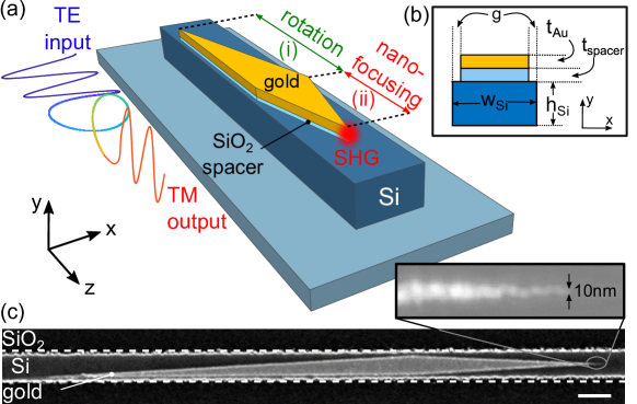
Our on-chip hybrid plasmonic integrated circuit (HPIC) is formed by two in-series plasmonic elements on a SOI waveguide (WG): a mode converter and a focusser. The latter combines a taper and a sharp tip, which functions as a nonlinear nanoscale light source. In our particular demonstration we probe second harmonic generation (SHG) in the visible from a near-infrared pump. Figure 1(a) shows a schematic of the HPIC. The first component (i) is formed by a polarization rotator Caspers et al. (2013) (also operating as a TE-photonic to TM-plasmonic mode converter Kim and Qi (2015)); the second (ii) is a nanofocusing gold tip Gramotnev and Bozhevolnyi (2010) resulting in SHG due to the intense nanoscale localization of the optical field, combined with the large surface of gold Butet et al. (2015). Figure 1(c) shows an electron micrograph of a fabricated HPIC on a SOI waveguide, highlighting the 10 nm tip sharpness, which is limited only by the gold grains generated during the evaporation process Doron-Mor et al. (2004).
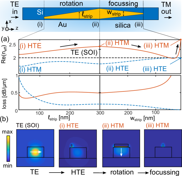
To analyze our circuit we first consider the relevant HPIC modes during propagation. Figure 2(a) shows the result of 2D finite element (FE) simulations (COMSOL) of the modal evolution along the HPIC. Figure 2(a) also shows a top-view schematic of Fig. 1 for clarity. In first instance, a gold film Johnson and Christy (1972) () with a spacer underneath Malitson (1965) () gradually extends on a silicon waveguide (, ) until complete coverage (here, ). The red line in Figure 2(a) shows how the hybrid-TE (HTE) mode evolves within the waveguide, in terms of the real effective index and loss. The input is the fundamental TE-SOI mode of the bare waveguide, which excites the HTE mode (i) that rotates into a hybrid-TM mode (HTM) (ii). The HTM mode is then converted to a deep-subwavelength HTM plasmonic mode (iii) Lafone et al. (2014) by reducing the gold strip width (). The Poynting vector associated with each participating mode is shown in Fig. 2(b), and presents the salient features of the evolution of TE-SOI mode after it couples to the HTE mode. The modal evolution of the equivalent HTM mode is shown as the blue curve in Fig. 2(a) for completeness. The TE-SOI waveguide mode excites both the HTE and HTM hybrid plasmonic eigenmodes in location (i), each evolving in a non-trivial way along the device.
We next calculate the performance of the full device using full 3D FE simulations. Due to the many parameters, materials, and functionalities involved, the optimization of the complete device is challenging: first, a suitable compromise between adiabaticity (requiring a slow modal transition, i.e., a long device length) and loss (requiring short device lengths) is required; secondly, small changes in geometric parameters, alignment, and surface roughness can have significant impact on the conversion efficiency. However, this process can be significantly simplified by using the modularity, which enables us to consider each element separately. In line with previous designs Caspers et al. (2013); Lafone et al. (2014) and to demonstrate a proof of concept, we have chosen the rotator length to be , and the focusser length to be , which by no means represent a fully optimized structure.
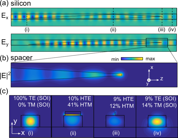
We model the fabricated structure shown in Fig. 1(c). The cross-section of the and field components in the middle of the Si-WG are shown in Fig. 3(a). Note in particular the polarization rotation in the spacer, manifesting as a vanishing component and an emerging component. A detailed plot of the electric field intensity within the spacer near the tip is shown in Fig. 3(b), showing a strong local enhancement at the tip apex. We calculate a intensity enhancement at the gold surface with with respect to the peak intensity in the silicon for the TE-SOI input. Figure 3(c) shows the power in each cross section as indicated by the dashed lines in Fig. 3(a)(i)–(iv). We calculate the conversion efficiency between the incoming TE-SOI mode and each of the participating modes in the full device by performing overlap integrals between the calculated 3D fields of Fig. 3(c) and the 2D modes of Fig. 2, as outlined in Ref. Kim and Qi (2015). We obtain a TE-to-HTM (rotator) conversion efficiency of 41 %, comparable to previous reports Caspers et al. (2013)), and a TE-to-HTM (nanofocus) conversion efficiency of , also comparable to the state of the art for plasmonic nanofocusing Nielsen et al. (2017). Note that 9% of the TE mode remains in the WG at output, which can be improved, for example, by more sophisticated multi-section rotator designs Chang and Feng (2017).
Fabrication and Linear Experiments
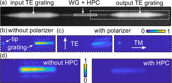
With an eye on the potential for modular approach to enhance off-the-shelf photonic waveguides with tailored plasmonic functionality, we purposefully choose to integrate our HPICs on previously fabricated SOI-WGs with standard electron-beam lithography and evaporation techniques. Figure 4 shows a microscope image of an example bare SOI-WG with length : light is coupled in- and out- of the waveguide with shallow gratings optimized for TE polarization. For further details of the bare SOI-WG design and characterization, see Methods and Supplementary Material. The HPIC nanostructures, shown in Fig. 1(c), were deposited on the WG in a subsequent step via combination of electron-beam lithography, /gold evaporation, and lift-off – note in particular the excellent quality of the gold film, the sharp tip obtained, and the high alignment precision ( resolution). The details of the HPIC fabrication procedure are presented in the Methods and in Supplementary Material. Preliminary experimental waveguide characterization in the near-infrared (NIR) was performed by coupling light from free space () onto the waveguide input grating coupler using a near-infrared microscope objective (NA = 0.85 - Olympus) and observing the light scattered by the device using a InGaAs camera (NIRvana, Princeton Instruments) (see Methods and Supplementary Material). The resulting measurement is shown in Fig. 4(b): we observe a diffraction-limited nanospot at the expected location of the gold nanotip, as well as residual TE light contained within the waveguide (in agreement with the simulations, see Fig. 3(a)(iv)), originating from the output grating. Figure 4(c) shows the same measurement when inserting a polarizer between the sample and camera with different orientations: we measure that the diffraction-limited spot is longitudinally (TM) polarized Tuniz et al. (2017), confirming polarization rotation and that light exiting the grating is TE polarized. As further confirmation, Fig. 4(d) shows a direct comparison of the amount of light exiting the grating in the presence of the HPIC, with respect to an adjacent control sample without the HPIC. From the ratio of the total power scattered by each TE grating under comparable input conditions (see Supplementary Material), we conclude that the residual light in the TE waveguide in the presence of the HPIC, relative to the bare SOI waveguide, is (, in agreement with 3D simulations (see Fig. 3(c)(iv)).
Nanofocusing and Nonlinear Enhancement
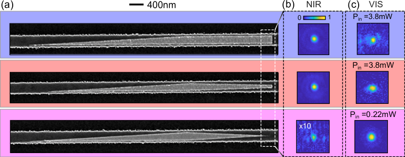
Plasmonic nanofocusing leads to spot sizes that are well below the diffraction limit, so that far-field linear optical experiments are inherently incapable of characterizing the focusing performance of our HPIC. Here we harness the high field intensities at the apex of the gold tip to estimate the field enhancement via nonlinear SHG experiments. Ultrashort pump pulses (, 200 fs, 80 MHz Diaz et al. (2016)) are coupled into the TE mode of the photonic waveguide via a grating coupler. They then enter one of three HPIC-enhanced WGs, each possessing incrementally sharper tips: the three HPIC considered here are shown in Fig. 5(a). Scattered light images by each HPIC captured using near-infrared (NIR) and visible (VIS) cameras (PIXIS – Princeton Instruments) are shown in Fig. 5(b) and 5(c), respectively. While nonlinear generation/scattering occurs during propagation across the entire HPIC de Hoogh et al. (2016), due the large absorption of silicon (approximately over at 660 nm Aspnes and Studna (1983)), the absence of phase matching, and the wavelength-scale propagation lengths considered, we can attribute the measured nonlinear signal only to the localized intensity at the edge of the gold tip from which the NIR light emerges. The spectra of the NIR pump and the visible radiation are shown in the inset of Fig. 6(a). The figure confirms that the visible radiation indeed is the second harmonic of the pump since . We observe that the sharpest tip causes the least amount of NIR scattering, consistent with 3D simulations (see Supplementary Material). In contrast, this tip also causes the strongest visible light emission (see Fig. 5(b),(c), magenta), even though the incident power is an order of magnitude smaller than in the other two cases – a preliminary indicator of nonlinear enhancement. In this case the input power is reduced by 10 times in order to avoid damaging the sharp due to the high field strength.
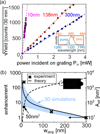
To quantify the nonlinear response of each tip, we measure the raw spectral yield versus incident power at the SHG wavelength, as shown in Fig. 6(a) (circles). The linear relationship between the square root of the yield and the average power incident on the sample (corresponding to a quadratic input power dependence, ), further confirms the mechanism of SHG. As a first conclusion we note the dramatic increase in SHG intensity for the sharpest tip, which indicates that nano-focusing was achieved. We compare the slopes of the three curves quantitatively via a linear fit to the experiment, as shown in the dashed lines of Fig. 6(a), and infer the relative intensity enhancement with respect to the strip. The results are summarized in Fig. 6(b), which shows the intensity enhancement as a function of the tip width obtained using different approaches. Black crosses show the measured enhancement, obtained by taking the square of the slopes in (Fig. 6(a)), normalized to . We experimentally observe a maximum intensity enhancement of for the sharpest gold tip relative to the gold strip. The theoretical enhancement at the tip is shown as a solid line in Fig. 6(b) (left axis), and was calculated using an adiabatic Eikonal approach Lafone et al. (2014), in excellent agreement with both the experiment and the range of intensity enhancements at the tip predicted by full 3D simulations (light blue region – see Supplementary Material for further details). Based on these results, the inferred effective mode area is Aspnes and Studna (1983) (black square).
Finally, we estimate the SHG conversion efficiency. After taking into account the effect of all optical elements, we conclude that the maximum SHG power is emitted by the sample for the sharpest nanotip (Fig. 6(a), magenta) is 2.3 fW for an incident power of 0.22 mW, corresponding to a net conversion efficiency of . Taking into account the coupling efficiency into the waveguide (14%, see Supplementary Material), this corresponds to of the power in the waveguide before the plasmonic rotator, and of the inferred power in the TM mode at the tip (cfr. Fig. 2(d)(ii)). Though these values are comparable to optimized nonlinear plasmonic SHG geometries Zhang et al. (2011); Butet et al. (2015), our geometry has the significant advantage of being on a PIC-compatible platform. It is worth noting that only of the power generated by a TM point source on the surface of a silicon waveguide radiates upwards, whereas the great majority of the SHG light is scattered into (and absorbed by) the silicon waveguide (see Supplementary Material). Future work will focus on new strategies to make use of the generated SHG, e.g., using hydrogenated amorphous silicon with low absorption at visible wavelengths, which will enable measurements of the SHG signal captured by the photonic waveguide Chen et al. (2017).
Discussion
The conversion efficiency could be further improved by optimizing the individual modular elements. Separate calculations for each module predict a peak rotator conversion efficiency of 58% for a rotator length of , and of 34% for a focusser length of (keeping all other parameters constant), resulting in a compound conversion efficiency of 20%. This in good agreement with equivalent calculations for the full device, predicting a maximum conversion efficiency of 24% for the same rotator- and focusser lengths of and , respectively. Thus, we estimate that through modest changes of the device parameters (e.g., increasing the gold thickness or with multi-section tapers Chang and Feng (2017) with up to 95% conversion efficiency), the pump TE-to-TM efficiency could be improved by approximately , which would lead to a 80-fold increase in nonlinear conversion efficiency. Further improvements may be achieved either by incorporating 2D materials on the waveguide surface, which possess a that is at least one order magnitude greater than gold surfaces Chen et al. (2017). Additionally, nonlinear effects such as third harmonic generation and four-wave-mixing may be accessed by placing highly nonlinear materials at the nanofocus Nielsen et al. (2017). Further enhancement may be achieved with additional plasmonic modules, such as a bowtie nanoantenna Peyskens et al. (2015) adjacent to the tip, or additional focuser and rotator modules which couple light back into the photonic waveguide.
This experiment represents the first PIC-compatible, integrated nonlinear-plasmonic-SHG nanoscale light source, that makes use of two, in-series hybrid-plasmonic circuit elements. This design, fabrication, and characterization represents the first TM plasmonic nano-focusser that is monolithically interfaced with an industry-standard TE-input SOI waveguide, and which can be coupled into by a conventional grating coupler. This work opens the door to the development of modular plasmonic circuit elements that can be seamlessly integrated on off-the-shelf photonic waveguides. This approach will facilitate access to efficient PIC-compatible deep-subwavelength field enhancements for on-chip quantum photonics and spectroscopy Tame et al. (2013), nonlinear Kravtsov et al. (2016) and atomic-scale Lee et al. (2019) sensing, and nanoscale terahertz sources and detectors Salamin et al. (2015).
Methods
Photonic waveguide grating design and characterization
The waveguide gratings were designed in-house using a 2D solver CAMFR Taillaert et al. (2006), with infinite air cladding and silicon substrate layer, a box layer if 2 thick, and a silicon waveguide layer of 220 nm, presenting grooves with an etching depth of and a period of . Here, and period , resulting in a high coupling efficiency (), and wide bandwidth centered in , low reflection (), and a selective in-coupling angle (). From images of the optimized coupling to the waveguide, referenced to a mirror, we obtain a grating coupling efficiency of 14%, assuming that the loss due to each grating is equal. Waveguide losses without the HPIC are measured to be 0.12 dB/ using waveguides of different lengths. See Supplementary Material for further details of the calculations, the calculated bandwidth, and experimental measurements of coupling- and propagation- losses.
Hybric plasmonic integrated circuit fabrication
The plasmonic HPICs are integrated on the SOI waveguides as follows. First, the silicon waveguides are spin-coated with PMMA resist, and the HPIC structures are written with standard electron-beam lithography (EBL) and developed with Methyl isobutyl ketone. 20 nm silica and 50 nm gold are subsequently coated with electron-beam evaporation. Finally, a lift-off step (Methyl-isobutyl-ketone) removes the resist. The alignment precision () is obtained using local gold markers, placed in the immediate vicinity of our off-the-shelf waveguides. See Supplementary Material for a schematic of the fabrication procedure and alignment markers used.
Experimental setup
A detailed schematic of the experimental setup is shown in Supplementary Material. The source is an Optical Parametric Oscillator (OPO) (, FWHM: 200 fs; repetition rate: 80 MHz). The power incident on the sample is controlled via a motorized half-waveplate (HWP) placed before a polarizer. The beam is spatially shaped using a beam expander, telescope, and elliptical lens, so that its profile matches that of the input waveguide grating. A beamsplitter (BSPM) and powermeter (PM) monitor the input power. A microscope holds the WGs and HPICs. Light is delivered and collected to the sample via a NIR microscope objective (Olympus, NA = 0.85) and BS. A short-pass filter (850 nm) is included in SHG experiments to filter out the NIR light. The scattered light is measured with an imaging spectrometer, using NIR (NIRvana) and VIS (PIXIS) cameras. An additonal NIR camera at a second output monitors alignment.
References
- Chrostowski and Hochberg (2015) L. Chrostowski and M. Hochberg, Silicon photonics design: from devices to systems (Cambridge U. Press, 2015).
- Dong et al. (2014) P. Dong, X. Liu, S. Chandrasekhar, L. L. Buhl, R. Aroca, and Y.-K. Chen, IEEE Journal of Selected Topics in Quantum Electronics 20, 150 (2014).
- Estevez et al. (2012) M. C. Estevez, M. Alvarez, and L. M. Lechuga, Laser & Photonics Reviews 6, 463 (2012).
- Marpaung et al. (2019) D. Marpaung, J. Yao, and J. Capmany, Nature Photonics 13, 80 (2019).
- Lipson (2005) M. Lipson, Journal of Lightwave Technology 23, 4222 (2005).
- Chen et al. (2009) L. Chen, K. Preston, S. Manipatruni, and M. Lipson, Optics Express 17, 15248 (2009).
- Zia et al. (2006) R. Zia, J. A. Schuller, A. Chandran, and M. L. Brongersma, Materials Today 9, 20 (2006).
- Taylor and Zijlstra (2017) A. B. Taylor and P. Zijlstra, ACS Sensors 2, 1103 (2017).
- Lee et al. (2019) J. Lee, K. T. Crampton, N. Tallarida, and V. A. Apkarian, Nature 568, 78 (2019).
- Gramotnev and Bozhevolnyi (2010) D. K. Gramotnev and S. I. Bozhevolnyi, Nature Photonics 4, 83 (2010).
- Kauranen and Zayats (2012) M. Kauranen and A. V. Zayats, Nature Photonics 6, 737 (2012).
- Li et al. (2018) G. Li, C. M. de Sterke, and S. Palomba, ACS Photonics 5, 1034 (2018).
- Kravtsov et al. (2016) V. Kravtsov, R. Ulbricht, J. M. Atkin, and M. B. Raschke, Nature Nanotechnology 11, 459 (2016).
- Nielsen et al. (2017) M. P. Nielsen, X. Shi, P. Dichtl, S. A. Maier, and R. F. Oulton, Science 358, 1179 (2017).
- de Hoogh et al. (2016) A. de Hoogh, A. Opheij, M. Wulf, N. Rotenberg, and L. Kuipers, ACS Photonics 3, 1446 (2016).
- Celebrano et al. (2015) M. Celebrano, X. Wu, M. Baselli, S. Großmann, P. Biagioni, A. Locatelli, C. De Angelis, G. Cerullo, R. Osellame, B. Hecht, et al., Nature Nanotechnology 10, 412 (2015).
- Lassiter et al. (2014) J. B. Lassiter, X. Chen, X. Liu, C. Ciracì, T. B. Hoang, S. Larouche, S.-H. Oh, M. H. Mikkelsen, and D. R. Smith, ACS Photonics 1, 1212 (2014).
- Butet et al. (2015) J. Butet, P.-F. Brevet, and O. J. Martin, ACS Nano 9, 10545 (2015).
- Oulton et al. (2008) R. F. Oulton, V. J. Sorger, D. Genov, D. Pile, and X. Zhang, Nature Photonics 2, 496 (2008).
- Alam et al. (2014) M. Z. Alam, J. S. Aitchison, and M. Mojahedi, Laser & Photonics Reviews 8, 394 (2014).
- Briggs et al. (2010) R. M. Briggs, J. Grandidier, S. P. Burgos, E. Feigenbaum, and H. A. Atwater, Nano Letters 10, 4851 (2010).
- Delacour et al. (2010) C. Delacour, S. Blaize, P. Grosse, J. M. Fedeli, A. Bruyant, R. Salas-Montiel, G. Lerondel, and A. Chelnokov, Nano Letters 10, 2922 (2010).
- Lin et al. (2012) C. Lin, H. M. K. Wong, B. Lau, M. A. Swilam, and A. S. Helmy, Applied Physics Letters 101, 123115:1 (2012).
- Melikyan et al. (2014) A. Melikyan, L. Alloatti, A. Muslija, D. Hillerkuss, P. C. Schindler, J. Li, R. Palmer, D. Korn, S. Muehlbrandt, D. Van Thourhout, et al., Nature Photonics 8, 229 (2014).
- Haffner et al. (2018) C. Haffner, D. Chelladurai, Y. Fedoryshyn, A. Josten, B. Baeuerle, W. Heni, T. Watanabe, T. Cui, B. Cheng, S. Saha, et al., Nature 556, 483 (2018).
- Kim et al. (2010) J. T. Kim, J. J. Ju, S. Park, M.-s. Kim, S. K. Park, and S.-Y. Shin, Optics Express 18, 2808 (2010).
- Sorger et al. (2011) V. J. Sorger, Z. Ye, R. F. Oulton, Y. Wang, G. Bartal, X. Yin, and X. Zhang, Nature Communications 2, 331 (2011).
- Luo et al. (2015) Y. Luo, M. Chamanzar, A. Apuzzo, R. Salas-Montiel, K. N. Nguyen, S. Blaize, and A. Adibi, Nano Letters 15, 849 (2015).
- Diaz et al. (2016) F. Diaz, T. Hatakeyama, J. Rho, Y. Wang, K. O’Brien, X. Zhang, C. M. de Sterke, B. Kuhlmey, and S. Palomba, Optics Express 24, 545 (2016).
- Caspers et al. (2013) J. N. Caspers, J. S. Aitchison, and M. Mojahedi, Optics Letters 38, 4054 (2013).
- Kim and Qi (2015) S. Kim and M. Qi, Optics Express 23, 9968 (2015).
- Doron-Mor et al. (2004) I. Doron-Mor, Z. Barkay, N. Filip-Granit, A. Vaskevich, and I. Rubinstein, Chemistry of Materials 16, 3476 (2004).
- Johnson and Christy (1972) P. D. Johnson and R. W. Christy, Physical Review B 6, 4370 (1972).
- Malitson (1965) I. Malitson, Journal of the Optical Society of America 55, 1205 (1965).
- Lafone et al. (2014) L. Lafone, T. P. Sidiropoulos, and R. F. Oulton, Optics Letters 39, 4356 (2014).
- Chang and Feng (2017) Y.-J. Chang and R.-W. Feng, Applied Optics 56, 5501 (2017).
- Tuniz et al. (2017) A. Tuniz, M. Chemnitz, J. Dellith, S. Weidlich, and M. A. Schmidt, Nano Letters 17, 631 (2017).
- Aspnes and Studna (1983) D. E. Aspnes and A. Studna, Physical Review B 27, 985 (1983).
- Zhang et al. (2011) Y. Zhang, N. K. Grady, C. Ayala-Orozco, and N. J. Halas, Nano Letters 11, 5519 (2011).
- Chen et al. (2017) H. Chen, V. Corboliou, A. S. Solntsev, D.-Y. Choi, M. A. Vincenti, D. De Ceglia, C. De Angelis, Y. Lu, and D. N. Neshev, Light: Science & Applications 6, e17060 (2017).
- Peyskens et al. (2015) F. Peyskens, A. Dhakal, P. Van Dorpe, N. Le Thomas, and R. Baets, ACS Photonics 3, 102 (2015).
- Tame et al. (2013) M. S. Tame, K. McEnery, Ş. Özdemir, J. Lee, S. Maier, and M. Kim, Nature Physics 9, 329 (2013).
- Salamin et al. (2015) Y. Salamin, W. Heni, C. Haffner, Y. Fedoryshyn, C. Hoessbacher, R. Bonjour, M. Zahner, D. Hillerkuss, P. Leuchtmann, D. L. Elder, et al., Nano Letters 15, 8342 (2015).
- Taillaert et al. (2006) D. Taillaert, F. Van Laere, M. Ayre, W. Bogaerts, D. Van Thourhout, P. Bienstman, and R. Baets, Japanese Journal of Applied Physics 45, 6071 (2006).
Acknowledgments
A.T. acknowledges support from the University of Sydney Fellowship Scheme. S.K. acknowledges support by the German Research Foundation (DFG) under Germany’s Excellence Strategy – EXC-2123/1. This work was performed in part at the NSW node of the Australian National Fabrication Facility (ANFF).
Author Contributions
A.T. conceived the idea and designed the experiment with input from S.P. and C.M.d.S. A.T. performed the simulations, experiments, and fabrication of the hybrid plasmonic circuit. O.B. designed the plasmonic device and fabricated the alignment markers. F.J.D. designed the bare silicon waveguides and the experimental setup. T.K., S.K. and E-B.K. fabricated the bare waveguides. A.T. and C.M.d.S wrote the manuscript with input from S.P. A.T., C.M.d.S. and S.P. directed the project.