Field-Effect Transistor based on Surface Negative Refraction in Weyl Nanowires
Abstract
Weyl semimetals are characterized by their bulk Weyl points – conical band touching points that carry a topological monopole charge – and Fermi arc states that span between the Weyl points on the surface of the material. Recently, significant progress has been made towards understanding and measuring the physical properties of Weyl semimetals. Yet, potential applications remain relatively sparse. Here, we propose Weyl semimetal nanowires as field-effect transistors, dubbed WEYLFETs. Specifically, applying gradient gate voltage along the nanowire, an electrical field is generated that effectively tilts the open surfaces, thus, varying the relative orientation between Fermi arcs on different surfaces. As a result, perfect negative refraction between adjacent surfaces can occur and longitudinal conductance along the wire is suppressed. The WEYLFET offers a high on/off ratio with low power consumption. Adverse effects due to dispersive Fermi arcs and surface disorder are studied.
Field-effect transistors (FETs) are electronic devices that use an electric field to control the flow of current through the device Galup-Montoro et al. (2007). There is a wide variety of materials and platforms used for various use cases of FETs; the majority thereof rely on semiconductor devices where the conduction channel can be switched off using an external gate. The conduction channel lies in the bulk of the semiconductor and early challenges in FET production concerned with surface passivation in order to overcome surface effects that prevented the gating from reaching the bulk Galup-Montoro et al. (2007). In parallel, low-power FETs’ applications are in constant development where new materials and reduced dimensionality of the conduction channel play a crucial role Javey et al. (2003); Schwierz (2010). Most recently, the progress of topological materials has opened a new avenue towards this goal based on the dissipationless chiral edge channels of the quantum anomalous Hall effect Haldane (1988); Liu et al. (2008); Yu et al. (2010); Hasan and Kane (2010); Qi and Zhang (2011); Chang et al. (2013); Liu et al. (2016); Chen et al. (2019a).
Weyl semimetals are a class of 3D materials with conduction and valence bands that linearly touch at isolated points of the bulk spectrum Wan et al. (2011); Murakami (2007); Burkov and Balents (2011); Wang et al. (2013); Weng et al. (2015); Huang et al. (2015). The touching points are so-called Weyl points, around which the electronic states can be effectively described by the Weyl equation Wan et al. (2011). Each Weyl point carries a monopole charge of Berry curvature, thus splitting momentum space into different regions of gapped spectra with different topology Wan et al. (2011); Yang et al. (2011). These unique bulk properties lead to electron chirality that offers potential applications as a bulk photovoltaic effect Chan et al. (2017); Osterhoudt et al. (2019).
In parallel, the nontrivial bulk topology has a corresponding boundary effect in the form of Fermi arcs that appear in the surface Brillouin zone Wan et al. (2011), which were recently observed experimentally Lv et al. (2015a); Xu et al. (2015a, b, c, 2016); Deng et al. (2016); Yang et al. (2015); Huang et al. (2016); Tamai et al. (2016); Jiang et al. (2017); Belopolski et al. (2016); Lv et al. (2015b). These arcs have an open cut at the chemical potential, leading to directional transport on the surface. Furthermore, depending on the orientation of the surface, the Fermi arcs are projected from the bulk Weyl points differently Chen et al. (2019b). This can lead to tunable surface configurations where negative refraction may occur between different surfaces of the material He et al. (2018).
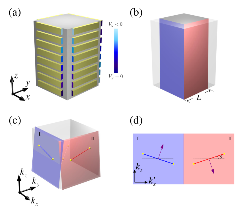
In this letter, we propose a new type of FET based on field-controlled surface negative refraction in a Weyl nanowire, or in short a WEYLFET. We consider a Weyl semimetal nanowire covered by isolated metal gates on top of each surface, see Fig. 1(a). By imposing a slanted electric potential along the nanowire, the redistribution of the electrons in the nanowire adjusts the bearings of the open surfaces, see Fig. 1(b). For nanowires with properly chosen surface bearings relative to the orientation of the bulk Weyl nodes, the electric potential results in an effective tilting of the Fermi arc in each surface Brillouin zone, see Fig. 1(c). Such relative tilting of Fermi arcs in the surface Brillouin zone can lead to perfect negative refraction between adjacent surfaces He et al. (2018); Chen et al. (2019b), see Fig. 1(d). The surface negative refraction considerably suppresses the conduction of electrons along the nanowire, i.e., for linear Fermi arcs, this effect produces a sharp electrically-tunable on/off switch of the conductance. We analyze the adverse impact of dispersive Fermi arcs, and the influence of surface disorder. Our proposal offers (i) a robust surface effect that does not necessitate passivation, (ii) reduced dissipation due to the backscattering-free channels, and (iii) a tunable sharp on/off switch, all of which make our proposed device a promising candidate for a low-power (WEYL-)FET.
In order to realize a WEYLFET with high on/off ratio, it is essential to have ideal Weyl semimetals Ruan et al. (2016a, b), in which the Fermi energy crosses both Weyl points and the transport is dominated by surface electrons. Furthermore, we consider sufficiently small tilting angles, such that reduction of the cross-section area of the nanowire is negligible. Hence, the main effect of the slanted gate voltage is the tilting of the orientation of the Fermi arcs, and the WEYLFET is controlled by the modulated surface transport.
Instead of studying nanowires with various surface bearings, we focus on the bulk Weyl nanowire with a general orientation of Weyl points, while retaining the same termination configuration of the nanowire. This approach is beneficial for the numerical study of the surface states Chen et al. (2019b). More concretely, we consider the minimal inversion ()-symmetric Weyl semimetal with two generally orientated Weyl points Chen et al. (2013). We start with a Weyl semimetal with two Weyl points at :
| (1) |
where , and are parameters, is the wave vector, and are Pauli matrices acting on the pseudospin space. The general orientation of Weyl points is achieved using the rotational transformation to the effective Hamiltonian , e.g., the rotation by an angle around the axis yields two Weyl points located at . We consider a nanowire along the -direction with a square cross section with side length , cf. Fig. 1(b). We take as the starting point in the absence of applied gate voltage . The gating results in rotation of the Weyl points with angle . It corresponds to a tilting of the Fermi arcs by an angle in the surface Brillouin zone Chen et al. (2019b) [Fig. 1(d)].
For convenience, we unfold the four open surfaces into the plane and label the longitudinal (transverse) momentum by (), see Fig. 1(d). The Fermi arcs on surfaces I and II can be described by the effective Hamiltonian
| (2) |
where is the in-plane momentum, is the velocity of the surface states, and “” corresponds to surfaces I and II, respectively. is the dispersion term, which introduces finite curvature to the Fermi arcs as in real materials. When , the straight Fermi arcs defined by have end points at for surface I, and at for surface II Chen et al. (2019b). The two Fermi arcs have opposite tilting, see Figs. 1(c) and (d). For a finite tilting angle (), the velocity in the -direction is inverted as the electrons transfer through the boundary between surfaces I and II, leading to negative refraction, see Fig. 1(d). This results in full suppression of electrons’ flow along the -direction. This is the key mechanism behind the WEYLFET, i.e., even infinitesimal gating should lead to an on/off control of the electronic transport.
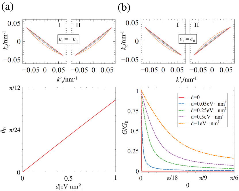
More realistically, Weyl semimetals exhibit dispersive Fermi arcs that depend on both bulk and surface details. Here, we consider a parabolic dispersion , where the overall sign of the dispersive correction on each surface can change. By tuning the dispersion strength , the Fermi arcs become curved [cf. Figs. 2(a) and (b)], as observed in real materials. Correspondingly, the electronic group velocities for the two surface states become k-dependent. The zero-energy single-spin conductance along the wire can be evaluated quasi-classically by
| (3) |
with
| (4) |
where the integral is taken over the incident states of surface I and the velocity is determined by the conservation of during the negative refraction. In the above expressions, is the surface density of states per unit area, is the average velocity in the -direction, and are the component of the Weyl points.
For the case of straight Fermi arcs () with , the conductance reduces to . As the Fermi arcs are tilted by a finite angle , we have and , which results in perfect negative refraction [cf. Fig. 1(d)]. As a result, the conductance is completely switched off by the gradient gate voltage, thus realizing a WEYLFET. This result also holds true when finite dispersion is added in the form of . In this case, due to the existence of reflection, the negative refraction is imperfect for small , and results in a finite switch-off angle , see Fig 2(a)ano .
We also investigate the case with equal dispersion, i.e., . In this case, the conductance becomes a function of the tilting angle , see Fig. 2(b)foo . decreases with , indicating the suppression of transport by negative refraction. Whereas for straight Fermi arcs, exhibits a sharp switch-off, as the dispersion strength increases, the current carried by refracted electrons cannot cancel out the incident current, resulting in a net current, which reduces the on/off ratio of the transistor for small .
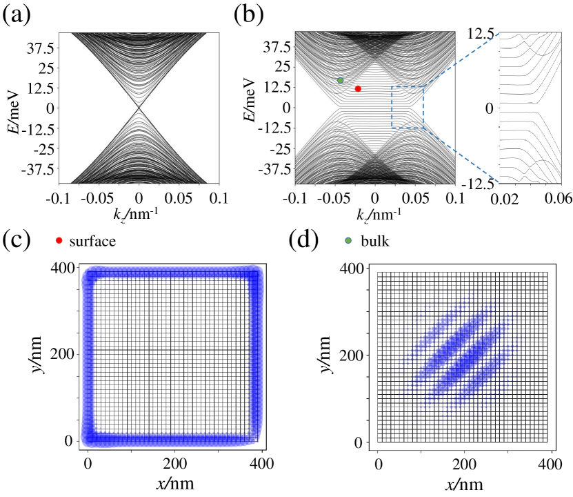
Complementary to the 2D surface negative refraction analysis above, the on/off switch of the WEYLFET conductance can be understood by studying the 1D band structure of the nanowire. We map the Hamiltonian (1) onto a cubic lattice through the substitutions , with being the lattice constant. We can then solve the model and plot its energy bands using KWANT Groth et al. (2014). In Fig. 3, we compare the resulting band structures with and without the tilt of the Fermi arcs. For , the energy bands contributed by the surface states are gapless, indicating a metallic phase. For finite tilting angle , a gap opening occurs for the surface states, and the conduction is switched off for small bias voltages. Therefore, under a small bias voltage, the WEYLFET corresponds to a gate-tunable gap closing and opening in the 1D picture, which is consistent with the 2D picture of negative refraction, cf. Fig. 1(d).
Next, we numerically calculate the conductance through the nanowire based on the cubic lattice model Groth et al. (2014). We introduce surface dispersion using an on-site potential on the surface layer; because the surface states have a k-dependent spatial distribution perpendicular to the surface, the on-site potential leads to a k-dependent potential, or equivalently to an effective dispersion of the Fermi arcs. The conductance along the nanowire as a function of the tilting angle of the Fermi arcs is shown in Figs. 4(a) and (b). In Fig. 4(a), the onsite potential takes opposite values on adjacent surfaces. Therefore, the dispersion on adjacent surfaces also takes opposite values, i.e., , and the on/off effect is confirmed. The angle at which the conductance is completely switched off increases with the onsite potential , because curved Fermi arcs imply that reflection processes exist in addition to negative refraction for small . Hence, in order to realize perfect negative refraction, the tilting angle must exceed a critical value, cf. Fig. 2(a). In Fig. 4(b), the onsite potential takes the same value on all surfaces, and the dispersions on the surfaces also become the same, i.e., . As a result, the on/off ratio is reduced as increases, which is in good agreement with the results in Fig. 2(b). Note that, here too, the surface dispersion has an adverse effect on the WEYLFET performance, which reduces the on/off ratio of the device. Therefore, in order to make a WEYLFET with high efficiency, it is preferable to use Weyl semimetals with weak and opposite surface dispersion. Recent experiments have realized Fermi arc manipulation by surface decoration Yang et al. (2019); Morali et al. (2019), which paves the way to realize our proposal.
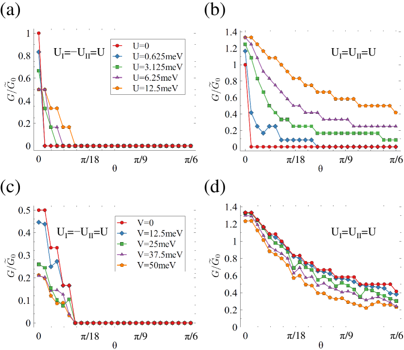
In real materials, surface roughness is unavoidable, and we simulate this effect by including surface disorder. For -symmetric Weyl semimetals, the corresponding chiral surface states imply that electronic transport is immune to surface disorder, i.e., the functionality of the WEYLFET should be robust to disorder. In Figs. 4(c) and (d), we present the calculated device conductance under different surface disorder strength for both dispersion configurations (). In both cases, the conductance decreases as surface disorder becomes stronger. This stems from the enhancement of backscattering that is induced by the disorder. However, the surface disorder has no effect on the switch-off region in Fig. 4(c), where perfect negative refraction occurs. In other words, the surface disorder has little effect on the functionality of the WEYLFET and the on/off ratio remains almost the same.
So far, we have solely analyzed a minimal -symmetric Weyl semimetal containing two Weyl points. Onto this minimal model, we have introduced the general principle of gate tunable Fermi arc tilting that can lead to negative refraction. Nevertheless, further work will analyze even more realistic situations, including (i) Weyl semimetals with multiple pairs of Weyl points, as in most of the materials Lv et al. (2015a); Xu et al. (2015a, b, c, 2016); Deng et al. (2016); Yang et al. (2015); Huang et al. (2016); Tamai et al. (2016); Jiang et al. (2017); Belopolski et al. (2016); Lv et al. (2015b); here the geometry of the nanowire should be properly chosen such that the overlap between the projections of different Fermi arcs to the -axis is minimized. Otherwise, the reflection at the boundary between different surfaces reduces the potency of negative refraction, and accordingly the on/off ratio of the WEYLFET. (ii) For time-reversal symmetric Weyl semimetals, the Fermi arc states are not chiral, leading to enhanced backscattering. In this case, we expect that surface disorder will have a stronger impact, and will reduce the on/off ratio of the WEYLFET. Hence, for the time-reversal symmetric Weyl semimetal, a nanowire with a clean surface is required for a high-efficiency WEYLFET. (iii) Another adverse effect can arise from the deviation of the Fermi level from the bulk Weyl points. In this case, bulk electrons participate in the transport and contribute an overall background to the conductance, which reduces the on/off ratio of the WEYLFET. At the same time, multiple scattering may occur in the bulk states, which also increases the dissipation of the WEYLFET. Furthermore, the finite bulk density of states also brings considerable screening effect, which reduces the efficiency of the slanted gate voltage. Based on these observations, ideal Weyl semimetals are needed for efficient WEYLFETs Ruan et al. (2016a, b), similar to their vital role in measuring other properties of Weyl semimetals. (iv) Finally, in many Weyl semimetals, the Fermi arcs’ dispersion is complex, making these surface states not much different from 2D normal metals, which cannot be used for WEYLFETs. Consequently, the material candidate for the WEYLFET should contain short Fermi arcs with small curvature Li et al. (2019); Wang et al. (2019); Soh et al. (2019).
In summary, we have explored a possible application of Weyl semimetal as a field-effect transistor (WEYLFET) that is based on electronic negative refraction between Fermi arcs on the surface of the device. By using the gradient gate along the Weyl nanowire, an on/off switch of the conductance can be achieved with a high ratio. Ideal Weyl semimetals with vanishing bulk density of states, chiral surface channels and small Fermi arc curvature can serve as good candidates for such high-efficiency WEYLFET with low-power consumption.
Acknowledgements.
We acknowledge financial support from the Swiss National Science Foundation (SNSF) through Division II and the Careers Division.References
- Galup-Montoro et al. (2007) Carlos Galup-Montoro et al., MOSFET modeling for circuit analysis and design (World scientific, 2007).
- Javey et al. (2003) Ali Javey, Jing Guo, Qian Wang, Mark Lundstrom, and Hongjie Dai, “Ballistic carbon nanotube field-effect transistors,” nature 424, 654 (2003).
- Schwierz (2010) Frank Schwierz, “Graphene transistors,” Nature nanotechnology 5, 487 (2010).
- Haldane (1988) F. D. M. Haldane, “Model for a quantum hall effect without landau levels: Condensed-matter realization of the ”parity anomaly”,” Phys. Rev. Lett. 61, 2015–2018 (1988).
- Liu et al. (2008) Chao-Xing Liu, Xiao-Liang Qi, Xi Dai, Zhong Fang, and Shou-Cheng Zhang, “Quantum anomalous hall effect in quantum wells,” Phys. Rev. Lett. 101, 146802 (2008).
- Yu et al. (2010) R. Yu, W. Zhang, H.-J. Zhang, S.-C. Zhang, X. Dai, and Z. Fang, “Quantized anomalous hall effect in magnetic topological insulators,” Science 329, 61–64 (2010).
- Hasan and Kane (2010) M Zahid Hasan and Charles L Kane, “Colloquium: topological insulators,” Reviews of modern physics 82, 3045 (2010).
- Qi and Zhang (2011) Xiao-Liang Qi and Shou-Cheng Zhang, “Topological insulators and superconductors,” Reviews of Modern Physics 83, 1057 (2011).
- Chang et al. (2013) C.-Z. Chang, J. Zhang, X. Feng, J. Shen, Z. Zhang, M. Guo, K. Li, Y. Ou, P. Wei, L.-L. Wang, Z.-Q. Ji, Y. Feng, S. Ji, X. Chen, J. Jia, X. Dai, Z. Fang, S.-C. Zhang, K. He, Y. Wang, L. Lu, X.-C. Ma, and Q.-K. Xue, “Experimental observation of the quantum anomalous hall effect in a magnetic topological insulator,” Science 340, 167–170 (2013).
- Liu et al. (2016) Chao-Xing Liu, Shou-Cheng Zhang, and Xiao-Liang Qi, “The quantum anomalous hall effect: Theory and experiment,” Annual Review of Condensed Matter Physics 7, 301–321 (2016).
- Chen et al. (2019a) Xi-Rong Chen, Wei Chen, L. B. Shao, and D. Y. Xing, “Engineering chiral edge states in two-dimensional topological insulator/ferromagnetic insulator heterostructures,” Phys. Rev. B 99, 085417 (2019a).
- Wan et al. (2011) Xiangang Wan, Ari M Turner, Ashvin Vishwanath, and Sergey Y Savrasov, “Topological semimetal and fermi-arc surface states in the electronic structure of pyrochlore iridates,” Physical Review B 83, 205101 (2011).
- Murakami (2007) Shuichi Murakami, “Phase transition between the quantum spin hall and insulator phases in 3d: emergence of a topological gapless phase,” New Journal of Physics 9, 356 (2007).
- Burkov and Balents (2011) A. A. Burkov and Leon Balents, “Weyl semimetal in a topological insulator multilayer,” Phys. Rev. Lett. 107, 127205 (2011).
- Wang et al. (2013) Zhijun Wang, Hongming Weng, Quansheng Wu, Xi Dai, and Zhong Fang, “Three-dimensional dirac semimetal and quantum transport in cd 3 as 2,” Physical Review B 88, 125427 (2013).
- Weng et al. (2015) Hongming Weng, Chen Fang, Zhong Fang, B. Andrei Bernevig, and Xi Dai, “Weyl semimetal phase in noncentrosymmetric transition-metal monophosphides,” Phys. Rev. X 5, 011029 (2015).
- Huang et al. (2015) Shin-Ming Huang, Su-Yang Xu, Ilya Belopolski, Chi-Cheng Lee, Guoqing Chang, BaoKai Wang, Nasser Alidoust, Guang Bian, Madhab Neupane, Chenglong Zhang, et al., “A weyl fermion semimetal with surface fermi arcs in the transition metal monopnictide taas class,” Nature communications 6, 7373 (2015).
- Yang et al. (2011) Kai-Yu Yang, Yuan-Ming Lu, and Ying Ran, “Quantum hall effects in a weyl semimetal: Possible application in pyrochlore iridates,” Phys. Rev. B 84, 075129 (2011).
- Chan et al. (2017) Ching-Kit Chan, Netanel H. Lindner, Gil Refael, and Patrick A. Lee, “Photocurrents in weyl semimetals,” Phys. Rev. B 95, 041104 (2017).
- Osterhoudt et al. (2019) Gavin B Osterhoudt, Laura K Diebel, Mason J Gray, Xu Yang, John Stanco, Xiangwei Huang, Bing Shen, Ni Ni, Philip JW Moll, Ying Ran, et al., “Colossal mid-infrared bulk photovoltaic effect in a type-i weyl semimetal,” Nature materials 18, 471 (2019).
- Lv et al. (2015a) BQ Lv, HM Weng, BB Fu, XP Wang, Hu Miao, Junzhang Ma, P Richard, XC Huang, LX Zhao, GF Chen, et al., “Experimental discovery of weyl semimetal taas,” Physical Review X 5, 031013 (2015a).
- Xu et al. (2015a) Su-Yang Xu, Ilya Belopolski, Nasser Alidoust, Madhab Neupane, Guang Bian, Chenglong Zhang, Raman Sankar, Guoqing Chang, Zhujun Yuan, Chi-Cheng Lee, et al., “Discovery of a weyl fermion semimetal and topological fermi arcs,” Science 349, 613–617 (2015a).
- Xu et al. (2015b) Su-Yang Xu, Nasser Alidoust, Ilya Belopolski, Zhujun Yuan, Guang Bian, Tay-Rong Chang, Hao Zheng, Vladimir N Strocov, Daniel S Sanchez, Guoqing Chang, et al., “Discovery of a weyl fermion state with fermi arcs in niobium arsenide,” Nature Physics 11, 748 (2015b).
- Xu et al. (2015c) Su-Yang Xu, Ilya Belopolski, Daniel S Sanchez, Chenglong Zhang, Guoqing Chang, Cheng Guo, Guang Bian, Zhujun Yuan, Hong Lu, Tay-Rong Chang, et al., “Experimental discovery of a topological weyl semimetal state in tap,” Science advances 1, e1501092 (2015c).
- Xu et al. (2016) Nan Xu, HM Weng, BQ Lv, Christian E Matt, Jihwey Park, Federico Bisti, Vladimir N Strocov, Dariusz Gawryluk, Ekaterina Pomjakushina, Kazimierz Conder, et al., “Observation of weyl nodes and fermi arcs in tantalum phosphide,” Nature communications 7, 11006 (2016).
- Deng et al. (2016) Ke Deng, Guoliang Wan, Peng Deng, Kenan Zhang, Shijie Ding, Eryin Wang, Mingzhe Yan, Huaqing Huang, Hongyun Zhang, Zhilin Xu, et al., “Experimental observation of topological fermi arcs in type-ii weyl semimetal mote 2,” Nature Physics 12, 1105 (2016).
- Yang et al. (2015) LX Yang, ZK Liu, Yan Sun, Han Peng, HF Yang, Teng Zhang, Bo Zhou, Yi Zhang, YF Guo, Marein Rahn, et al., “Weyl semimetal phase in the non-centrosymmetric compound taas,” Nature physics 11, 728 (2015).
- Huang et al. (2016) Lunan Huang, Timothy M McCormick, Masayuki Ochi, Zhiying Zhao, Michi-To Suzuki, Ryotaro Arita, Yun Wu, Daixiang Mou, Huibo Cao, Jiaqiang Yan, et al., “Spectroscopic evidence for a type ii weyl semimetallic state in mote 2,” Nature materials 15, 1155 (2016).
- Tamai et al. (2016) Anna Tamai, QS Wu, Irène Cucchi, Flavio Yair Bruno, Sara Riccò, TK Kim, M Hoesch, Céline Barreteau, Enrico Giannini, Céline Besnard, et al., “Fermi arcs and their topological character in the candidate type-ii weyl semimetal mote 2,” Physical Review X 6, 031021 (2016).
- Jiang et al. (2017) Juan Jiang, ZK Liu, Y Sun, HF Yang, CR Rajamathi, YP Qi, LX Yang, C Chen, H Peng, CC Hwang, et al., “Signature of type-ii weyl semimetal phase in mote 2,” Nature communications 8, 13973 (2017).
- Belopolski et al. (2016) Ilya Belopolski, Daniel S Sanchez, Yukiaki Ishida, Xingchen Pan, Peng Yu, Su-Yang Xu, Guoqing Chang, Tay-Rong Chang, Hao Zheng, Nasser Alidoust, et al., “Discovery of a new type of topological weyl fermion semimetal state in mo x w 1- x te 2,” Nature communications 7, 13643 (2016).
- Lv et al. (2015b) BQ Lv, N Xu, HM Weng, JZ Ma, P Richard, XC Huang, LX Zhao, GF Chen, CE Matt, F Bisti, et al., “Observation of weyl nodes in taas,” Nature Physics 11, 724 (2015b).
- Chen et al. (2019b) Guangze Chen, Wei Chen, and Oded Zilberberg, “Negative refraction in fermi arc surface states of weyl semimetals,” in preparation (2019b).
- He et al. (2018) Hailong He, Chunyin Qiu, Liping Ye, Xiangxi Cai, Xiying Fan, Manzhu Ke, Fan Zhang, and Zhengyou Liu, “Topological negative refraction of surface acoustic waves in a weyl phononic crystal,” Nature 560, 61 (2018).
- Ruan et al. (2016a) Jiawei Ruan, Shao-Kai Jian, Hong Yao, Haijun Zhang, Shou-Cheng Zhang, and Dingyu Xing, “Symmetry-protected ideal weyl semimetal in hgte-class materials,” Nature communications 7, 11136 (2016a).
- Ruan et al. (2016b) Jiawei Ruan, Shao-Kai Jian, Dongqin Zhang, Hong Yao, Haijun Zhang, Shou-Cheng Zhang, and Dingyu Xing, “Ideal weyl semimetals in the chalcopyrites , , , and ,” Phys. Rev. Lett. 116, 226801 (2016b).
- Chen et al. (2013) Wei Chen, Liang Jiang, R Shen, L Sheng, BG Wang, and DY Xing, “Specular andreev reflection in inversion-symmetric weyl semimetals,” EPL (Europhysics Letters) 103, 27006 (2013).
- (38) The switch-off angle is given by for the effective Hamiltonian Eq.(2).
- (39) For curved Fermi arcs and small , there exist reflection processes in addition to the negative refraction. Here, the reflection does not change , and we calculate by , where seperates the Fermi arc into two segments which lead to negative refraction and reflection, respectively.
- Groth et al. (2014) Christoph W Groth, Michael Wimmer, Anton R Akhmerov, and Xavier Waintal, “Kwant: a software package for quantum transport,” New Journal of Physics 16, 063065 (2014).
- Yang et al. (2019) HF Yang, LX Yang, ZK Liu, Y Sun, C Chen, H Peng, M Schmidt, D Prabhakaran, BA Bernevig, C Felser, et al., “Topological lifshitz transitions and fermi arc manipulation in weyl semimetal nbas,” Nature communications 10, 1–7 (2019).
- Morali et al. (2019) Noam Morali, Rajib Batabyal, Pranab Kumar Nag, Enke Liu, Qiunan Xu, Yan Sun, Binghai Yan, Claudia Felser, Nurit Avraham, and Haim Beidenkopf, “Fermi-arc diversity on surface terminations of the magnetic weyl semimetal co3sn2s2,” arXiv preprint arXiv:1903.00509 (2019).
- Li et al. (2019) Jiaheng Li, Yang Li, Shiqiao Du, Zun Wang, Bing-Lin Gu, Shou-Cheng Zhang, Ke He, Wenhui Duan, and Yong Xu, “Intrinsic magnetic topological insulators in van der waals layered mnbi2te4-family materials,” Science Advances 5, eaaw5685 (2019).
- Wang et al. (2019) Lin-Lin Wang, Na Hyun Jo, Brinda Kuthanazhi, Yun Wu, Robert J. McQueeney, Adam Kaminski, and Paul C. Canfield, “Single pair of weyl fermions in the half-metallic semimetal ,” Phys. Rev. B 99, 245147 (2019).
- Soh et al. (2019) J-R Soh, F de Juan, MG Vergniory, NBM Schröter, MC Rahn, DY Yan, M Bristow, PA Reiss, JN Blandy, YF Guo, et al., “An ideal weyl semimetal induced by magnetic exchange,” arXiv preprint arXiv:1901.10022 (2019).