First-principles study of point defects in LiGaO2
Abstract
The native point defects are studied in LiGaO2 using hybrid functional calculations. We find that the relative energy of formation of the cation vacancies and the cation antisite defects depends strongly on the chemical potential conditions. The lowest energy defect is found to be the Ga donor. It is compensated mostly by and in part by Li in the more Li-rich conditions. The equilibrium carrier concentrations are found to be negligible because the Fermi level is pinned deep in the gap and this is consistent with insulating behavior in pure LiGaO2. The has high energy under all reasonable conditions. Both the GaLi and the are found to be negative centers with deep transition levels.
I Introduction
Recently, there has been an interest in ultra-wide-band-gap semiconductors such as -Ga2O3 because of their potential in pushing high-power transitions to the next level of performance.Sasaki et al. (2013); Green et al. (2016) An important figure of merit for such applications is the breakdown field and the latter is directly correlated with the band gap. Here we draw attention to an even higher band gap material, LiGaO2. LiGaO2 has a wurtzite-derived crystal structureMarezio (1965); Ishii, Tazoh, and Miyazawa (1998) and band gap of 5.3-5.6 eV (at room temperature) based on optical absorptionWolan and Hoflund (1998); Johnson, McLeod, and Moewes (2011); Ohkubo et al. (2002); Chen et al. (2014) but potentially even as large as 6.25 eV (at ) based on quasi-particle self-consistent (QS) calculations,Boonchun and Lambrecht (2011a) with the one-particle Green’s function and the screened Coulomb potential. It can be thought of as a I-III-VI2 ternary analog of wurtzite ZnO, in which each group II Zn atom is replaced by either a group-I Li or a group III-Ga in a specific ordered pattern with the spacegroup. In this structure the octetrule is satisfied because each O is surrounded tetrahedrally by two Li and two Ga. The prototype for this crystal structure is -NaFeO2. LiGaO2 can be grown in bulk form by the Czochralsky methodMarezio (1965) and because of its good lattice match has been explored as a substrate for GaN. It can also be grown by epitaxial methods on ZnO and vice versa. Mixed ZnO-LiGaO2 alloys have been reported.Omata et al. (2008, 2011) It has been considered for piezoelectric properties,Nanamatsu, Doi, and Takahashi (1972); Gupta et al. (1976); Boonchun and Lambrecht (2010) and is naturally considered as a wide gap insulator. However, Boonchun and Lambrecht Boonchun and Lambrecht (2011b) suggested it might be worthwhile considering as a semiconductor electronic material and showed in particular that it could possibly be n-type doped by Ge. That study only used the 16 atom primitive unit cell of LiGaO2 and thus considered rather high (25 %) GeGa doping or MgLi doping. It did not study the site competition or native defect compensation issues. Here we study the native point defects by means of hybrid functional supercell calculations.
II Computational Method
Our study is based on density functional calculations using the Heyd-Scuseria-Ernzerhof (HSE) hybrid functional.Heyd, Scuseria, and Ernzerhof (2003, 2006) The calculations are performed using the Vienna Ab-Initio Simulation Package (VASP). VAS ; Kresse and Furthmiiller (1996) The electron ion interactions are described by means of the Projector Augmented Wave (PAW) method.Blöchl (1994); Kresse and Joubert (1999) We use a well-converged energy cut-off of 500 eV for the projector augmented plane waves. We performed the calculations with a supercell size of 128 atoms (which corresponds to the primitive unit cell) and a single k-point shifted away from is employed for the Brillouin zone integration. The valence configurations used were for Li, for Ga and for O. In the HSE functional, the Coulomb potential in the exchange energy is divided into short-range and long-range parts with a screening length of 10 Å and only the short-range part of the exact Hartree-Fock non-local exchange is included by mixing it with the generalized gradient Perdew-Burke-Enrzerhof (PBE) potential with a mixing fraction . The band gap obtained in this way ( eV) is still slightly lower than the experimental value.
III Results
The energy of formation of the defect in charge state is given by
| (1) |
where is the total energy of the supercell containing the defect and is the total energy of the perfect crystal supercell. The chemical potentials represent the energy for adding or removing atoms from the crystal to a reservoir in the process of making the defect. The is the change in number of atoms of species . Likewise the chemical potential of the electron determining its charge state is with the energy of an electron at the valence band maximum (VBM) relative to the average electrostatic potential in bulk and the Fermi energy in the gap measured from the VBM. The alignment potential represents the alignment of the average electrostatic potential in the supercell far away from the defect relative to that in the bulk. This is calculated using the Freysoldt et al. approach.Freysoldt, Neugebauer, and Van de Walle (2009); Freysoldt et al. (2014) The final term is the image charge correction term which corrects for the Madelung energy of the periodic array of net defect point charges in the uniform background that is added to ensure overall charge neutrality when considering a locally charged defect state. It is closely related to the alignment potential and including these corrections allows one to extrapolate the energy of formation to the dilute limit of an infinitely large supercell.
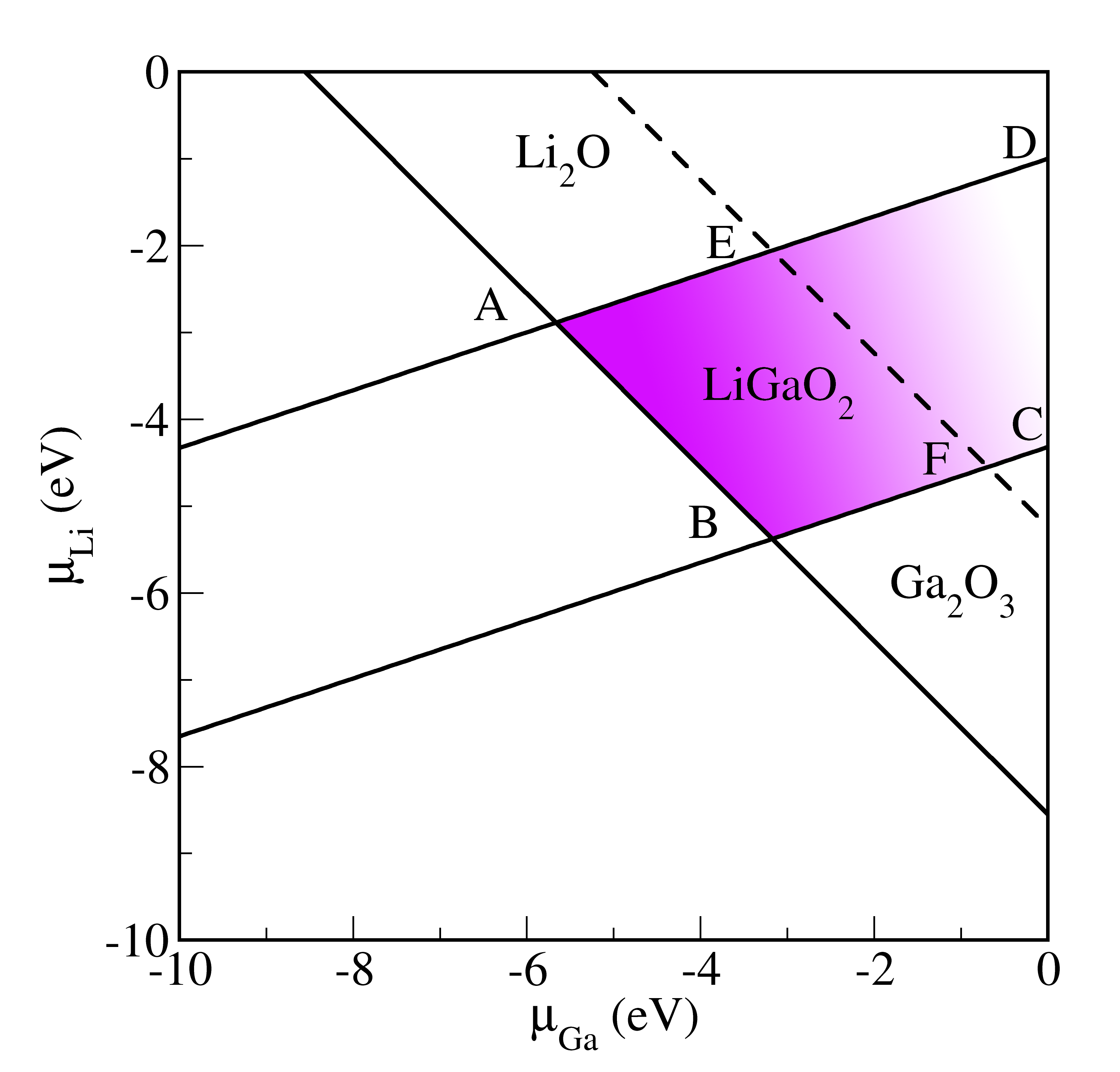
The chemical potentials , where are the chemical potentials of each species in its reference state, namely the phase it occurs in at standard pressure and room temperature, and are the excess chemical potentials. The latter are viewed as a tunable parameter reflecting the growth conditions but must obey certain restrictions based on thermodynamic equilibrium. These include
| (2) |
where is the energy of formation of LiGaO2, which we calculated to be eV. Each of the excess chemical potentials on the left must be less than zero in order to avoid precipitation of the bulk elements Li and Ga or evolving O2 gas. For example, corresponds to metallic body-centered-cubic Li and thus corresponds to the assumption that the crystal with the defect is in equilibrium with bulk metallic Li as reservoir. Similarly corresponds to equilibrium with metallic bulk Ga and corresponds to O in the O2 molecule. However, we need to also consider further restrictions imposed by competing binary compounds Ga2O3 and Li2O.
| (3) |
These restrictions determine the region of chemical potentials in which LiGaO2 is stable relative to the competing binaries and elements. They are bounded by
| (4) |
with eV and eV.
It is represented in the phase diagram shown in Fig. 1. The points correspond respectively to (A) Li-rich, Ga-poor, (B) Li-poor as well as relative Ga-poor, (C) Ga-rich, Li-poor and (D) Ga-rich and Li-rich but O-poor. The shading of the color is darker the higher the chemical potential of O and the line corresponds to the O-rich limit . In addition to the extreme chemical potential conditions (Ga-rich and Li-rich), we consider an intermediate oxygen chemical potential corresponding to a realistic growth condition during the annealing of LiGaO2. The oxygen chemical potential is a function of temperature and oxygen partial pressure, as described by Reuter et al. Reuter and Scheffler (2001)
| (5) |
where is the oxygen chemical potential at the standard pressure atm, is Boltzmann’s constant, and is the temperature in Kelvin. In the growth experiment of Ref. Chen et al., 2014, the mixed and powders were compressed into tablets and then calcined at 1200 for 20 h in air.Chen et al. (2014) We therefore choose an annealing temperature of 1200 and an oxygen partial pressure of 0.21 atm which represents the ratio of oxygen gas in ambient environment. The growth conditions at annealing temperature of 1200 and oxygen partial pressure of 0.21 atm is represented by the dashed line in Fig. 1.
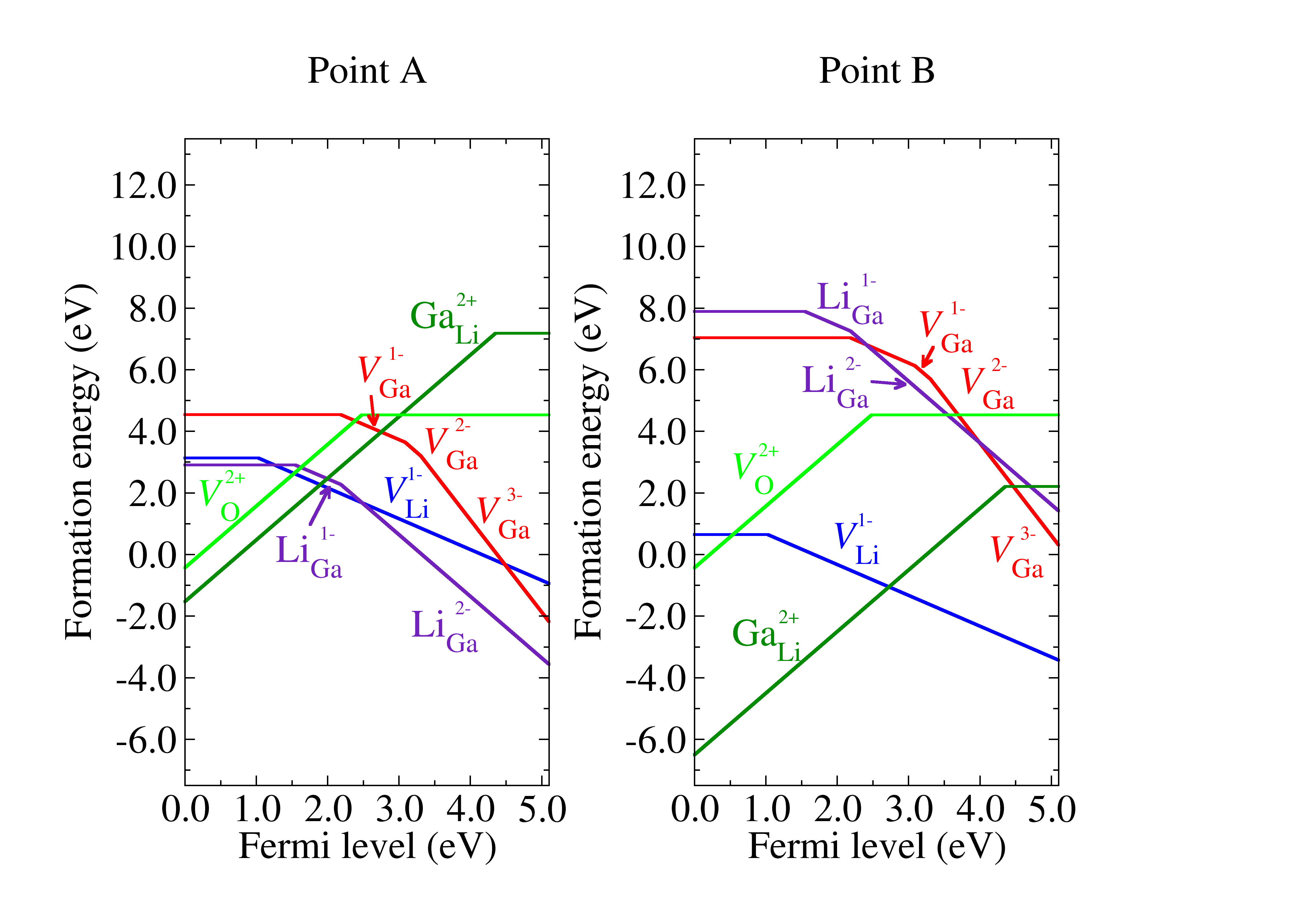
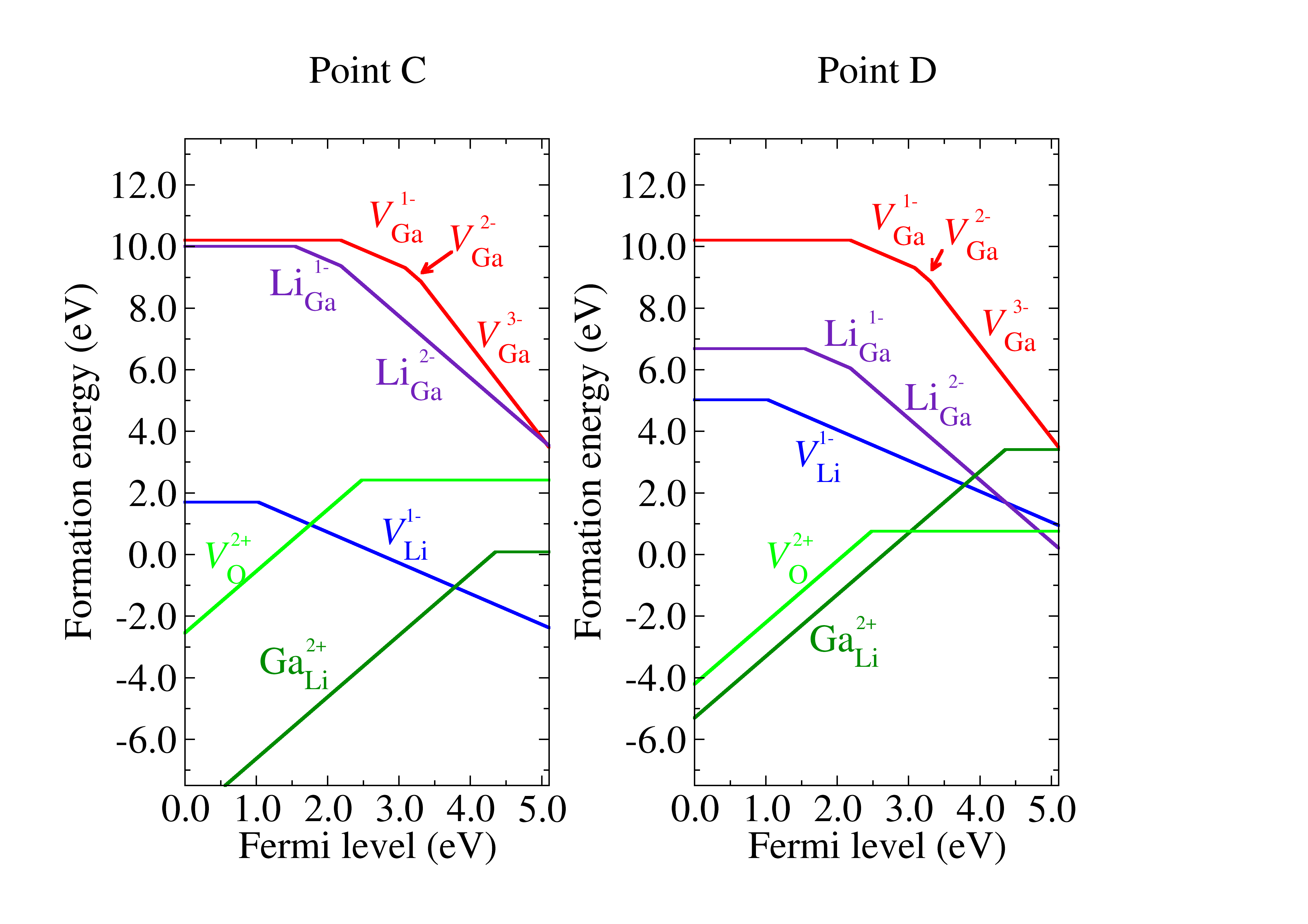
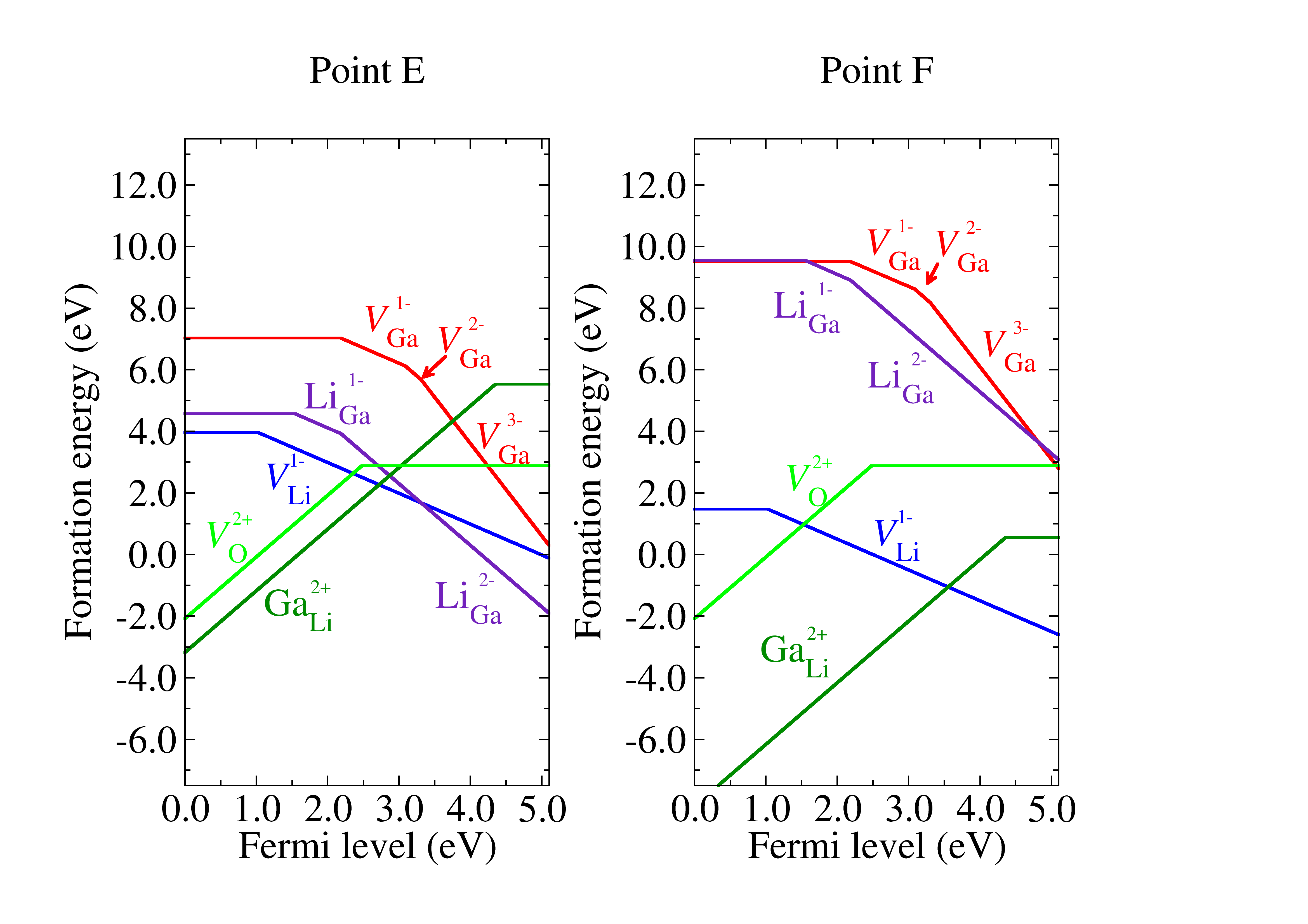
The defects considered are the vacancies , and and the antisites LiGa and GaLi. The effects of spin polarization were included for cases with unpaired electrons in defect levels. Interstitial defects will be considered in the future but comparison with II-IV-N2 semiconductors suggest that they would be of high energy.Skachkov et al. (2016); Skachkov and Lambrecht (2017) The defect energies of formation are shown for the six chemical potential points and in Fig. 2.
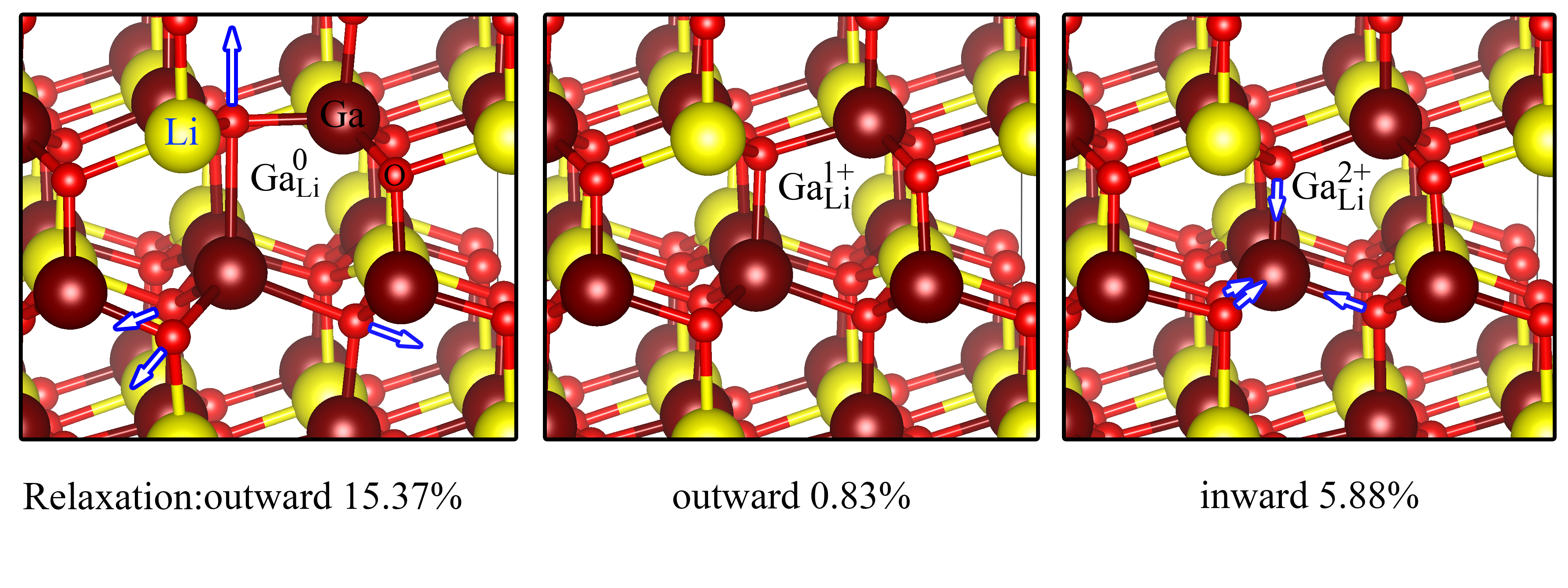
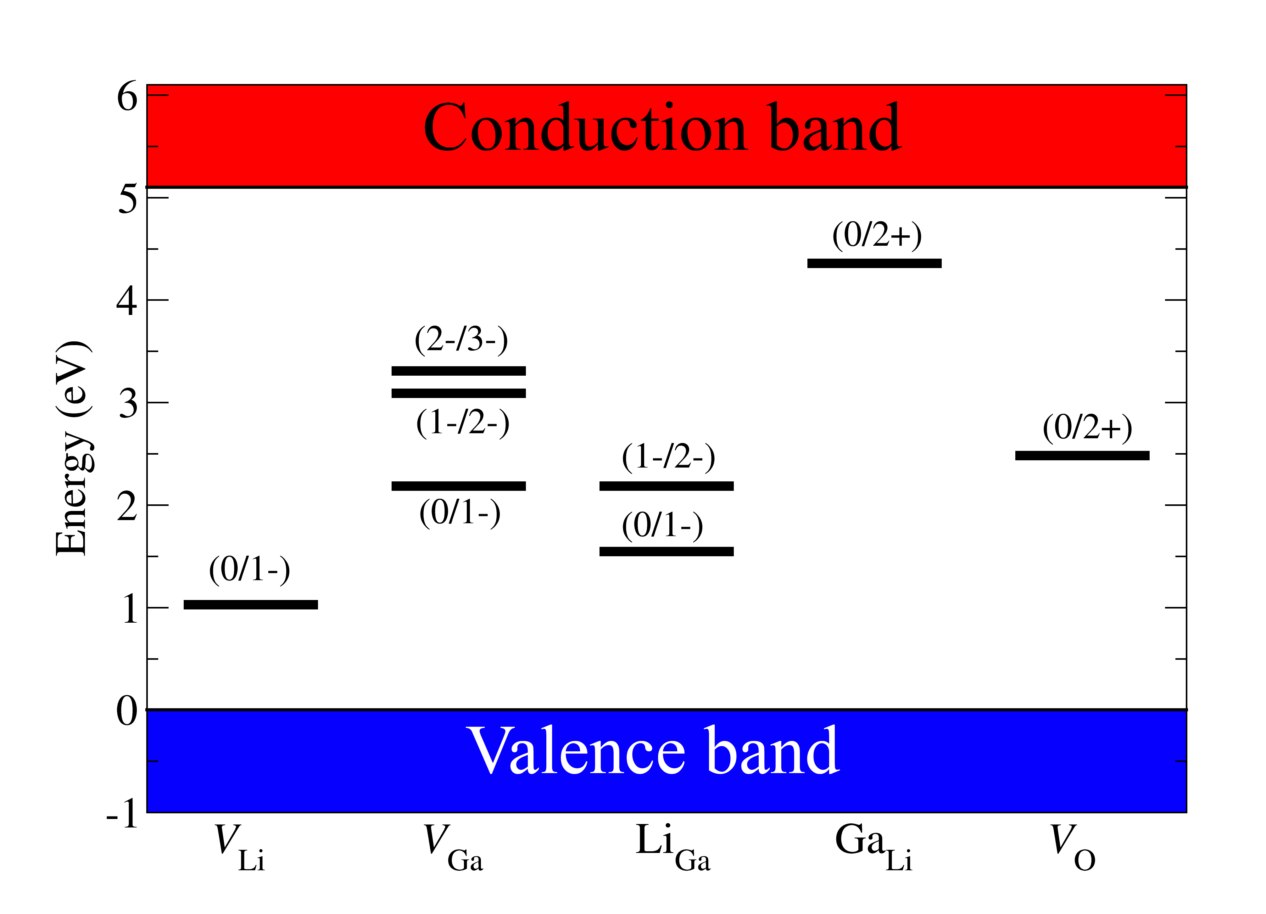
First we see that GaLi is the lowest energy defect for in all cases. It is a double donor, which is in the charge state over most of the gap. Still, it has a well-defined transition making it a negative system. In Fig. 3 we can see that while for the neutral charge state, the O around GaLi move outward, they move inward for the charge state with an in-between outward relaxation for the state. The additional stabilization by outward motion of the O when adding two electrons rather than one causes the negative behavior where the charge state is never the lowest energy one for any Fermi level position. It is thus not behaving like a simple shallow donor, consistent with the relatively deep donor binding energy of 0.74 eV below the conduction band minimum (CBM). We thus do not expect it to be an effective n-type dopant. We can see that this defect has negative energy of formation at in most cases. This reflects that even in the most Ga-poor case, this defect is hard to avoid because we cannot make the system poor enough in Ga without reaching the stability limit imposed by Li2O. On the other hand, a Fermi level is not expected to be realistic as discussed later.
The LiGa antisite on the other hand is a double acceptor which can occur in charge states. It is the lowest energy defect in its charge state near the CBM in cases , and . These are the cases richest in Li.
As for the vacancies, occurs in charge states, while occurs in charge states. We can see that has a high energy of formation in all cases. Although its negative charge states have significantly lower energy for close to the CBM, it never becomes the lowest energy defect and therefore does not play a role in determining the Fermi level. The is more interesting. Although it has high energy in the Li-rich case (which is somewhat unrealistic and O-poor) it has low energy in the Li-poor cases, . Even in case , its intersection with the Ga occurs close to that of the intersection of the latter with Li. We thus expect that both these acceptors may play a role in compensating the Ga.
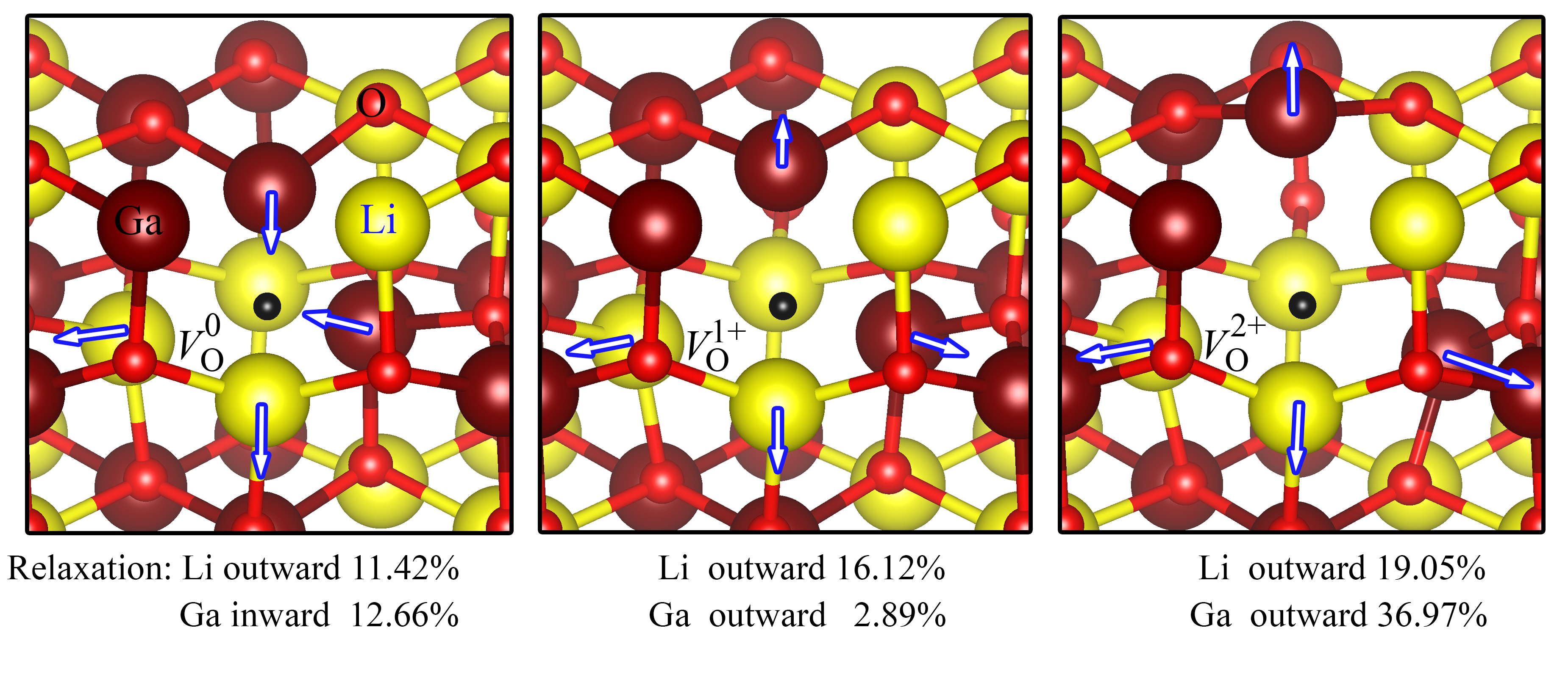
Turning now to the O-vacancies, there are two non-equivalent sites for the oxygen in LiGaO2: on top of Li (O1) or on top of Ga (O2). We find that both and are only stable in the neutral and charge states (with slightly lower in energy than ) with the transition level (2+/0) at 2.48 eV above the VBM or 2.62 eV below the CBM. This is a quite deep donor level and indicates that the vacancy is also a negative center. In Fig. 4 one can see that also in this case the relaxations are strongly charge-state dependent. This figure shows the relaxations near a but similar results hold for . In the neutral charge state, the Ga move inward, while the Li move outward. In the state both move strongly outward. This is similar to the in ZnOBoonchun and Lambrecht (2011b, 2013) although the level is here even deeper and close to mid gap. We find that the energy of formation is negative for Fermi levels close to the VBM for points . They become positive for the O-rich limits (, ). Its energy of formation is always higher than that of the Ga and thus it is not expected to play a significant role in the charge balance.
Using the charge neutrality condition between free electron concentration , free hole concentration and the various defect concentrations,
| (6) |
where is the number of available sites per cm3 and a degeneracy factor depending on the charge state, we can find the equilibrium Fermi level and the defect concentrations for a given temperature following the procedure of Ref.Skachkov et al., 2016. For the electron and hole concentrations we use a parabolic band with effective density of states masses and (as obtained from the calculate hybrid functional band structure and averaging over directons.) For a temperature of K close to the growth temperature, we find that under chemical potential conditions , the equilibrium Fermi level is eV, close to the intersection of the and Ga. The electron concentration cm-3 but the cm-3 are unrealistically high. This is related to the energies of formation of the main defects GaLi and being negative for the equilibrium Fermi level. For point , the equilibrium Fermi level position is closer to mid gap, eV with , and cm-3, cm-3. So, in this case the concentrations of defects are much smaller and the Ga is still mostly compensated by but partially also by Li. The electron concentration at cm-3 is then only slightly higher than the hole concentration cm-3 but both free carrier concentrations are in fact negligible under both chemical potential conditions considered. Even under the most Ga-poor conditions (point ), Ga is the dominant defect and is compensated mostly by . In this case, eV is closest to the VBM and the material would then be slightly -type with cm-3.
| Defect | ||
|---|---|---|
| (0/1-) | 1.0270 | |
| (0/1-) | 2.1843 | |
| (1-/2-) | 3.0899 | |
| (2-/3-) | 3.3088 | |
| (0/1-) | 1.5464 | |
| (1-/2-) | 2.1855 | |
| (0/2+) | 4.3569 | |
| (0/2+) | 2.4831 |
It is instructive to compare the defect physics in this system to that in II-IV-N2 semiconductors like ZnGeN2,Skachkov et al. (2016). The similarity is that in both cases, the antisites play a crucial role. However, the dependence on chemical potentials of the elements is more important here because a wider region of stability occurs. Furthermore the GaLi antisite is here not a shallow but a deep donor and is thus not expected to lead to unintentional n-type doping. This is consistent with the insulating behavior of LiGaO2. However, it does not exclude the possibility of n-type doping by Si or Ge or Sn which will be studied separately.
IV Conclusions
In this paper we have studied the native defects in LiGaO2. We find that the relative energy of formation of vacancies and antisites depends strongly on the chemical potential conditions. The GaLi antisite is a dominant donor defect. However, it has a rather deep donor level and is a negative center. It is thus not expected to lead to significant n-type doping. It furthermore becomes compensated mostly by and in part by Li depending on how rich the system is in Li. The is found to be an even deeper double donor negative center. The defect transition levels are all relatively deep in to the gap with no truly shallow levels.
Acknowledgements.
The work at CWRU was supported by the U.S. National Science Foundation under grant No. 1755479. The work at Kasetsart was supported by Kasetsart University Research and Development Institute (KURDI).References
- Sasaki et al. (2013) K. Sasaki, M. Higashiwaki, A. Kuramata, T. Masui, and S. Yamakoshi, “”{MBE} grown ga2o3 and its power device applications ”,” J. Cryst. Growth 378, 591 – 595 (2013), the 17th International Conference on Molecular Beam Epitaxy.
- Green et al. (2016) A. J. Green, K. D. Chabak, E. R. Heller, R. C. Fitch, M. Baldini, A. Fiedler, K. Irmscher, G. Wagner, Z. Galazka, S. E. Tetlak, A. Crespo, K. Leedy, and G. H. Jessen, “3.8-MV/cm Breakdown Strength of MOVPE-Grown Sn-Doped -Ga2O3 MOSFETs,” IEEE Electron Device Letters 37, 902–905 (2016).
- Marezio (1965) M. Marezio, “The crystal structure of LiGaO2,” Acta Crystallographica 18, 481–484 (1965).
- Ishii, Tazoh, and Miyazawa (1998) T. Ishii, Y. Tazoh, and S. Miyazawa, “Single-crystal growth of LiGaO2 for a substrate of GaN thin films,” J. Crystal Growth 186, 409 – 419 (1998).
- Wolan and Hoflund (1998) J. T. Wolan and G. B. Hoflund, “Chemical alteration of the native oxide layer on ligao2(001) by exposure to hyperthermal atomic hydrogen,” J. Vac. Sci. Tech. A 16, 3414–3419 (1998).
- Johnson, McLeod, and Moewes (2011) N. W. Johnson, J. A. McLeod, and A. Moewes, “The electronic structure of lithium metagallate,” Journal of Physics: Condensed Matter 23, 445501 (2011).
- Ohkubo et al. (2002) I. Ohkubo, C. Hirose, K. Tamura, J. Nishii, H. Saito, H. Koinuma, P. Ahemt, T. Chikyow, T. Ishii, S. Miyazawa, Y. Segawa, T. Fukumura, and M. Kawasaki, “Heteroepitaxial growth of β-ligao2 thin films on zno,” Journal of Applied Physics 92, 5587–5589 (2002).
- Chen et al. (2014) C. Chen, C.-A. Li, S.-H. Yu, and M. M. Chou, “Growth and characterization of -LiGaO2 single crystal,” Journal of Crystal Growth 402, 325 – 329 (2014).
- Boonchun and Lambrecht (2011a) A. Boonchun and W. R. L. Lambrecht, “Electronic structure, doping, and lattice dynamics of LiGaO2,” in Oxide-based Materials and Devices II, Proceedings of SPIE, Vol. 7940, edited by F. H. Terani, D. C. Look, and D. J. Rogers (2011) p. 79400N.
- Omata et al. (2008) T. Omata, K. Tanaka, A. Tazuke, K. Nose, and S. Otsuka-Yao-Matsuo, “Wide band gap semiconductor alloy: x(LiGaO2)1â2â(1âx)ZnO,” J. Appl. Phys. 103, 083706 (2008).
- Omata et al. (2011) T. Omata, M. Kita, K. Nose, K. Tachibana, and S. Otsuka-Yao-Matsuo, “Zn2LiGaO4, Wurtzite-Derived Wide Band Gap Oxide,” Jpn. J. Appl. Phys. 50, 031102 (2011).
- Nanamatsu, Doi, and Takahashi (1972) S. Nanamatsu, K. Doi, and M. Takahashi, “Piezoelectric, elastic and dielectric properties of LiGaO2,” Japanese Journal of Applied Physics 11, 816–822 (1972).
- Gupta et al. (1976) S. N. Gupta, J. F. Vetelino, V. B. Jipson, and J. C. Field, “Surface acoustic wave properties of lithium gallium oxide,” Journal of Applied Physics 47, 858–860 (1976).
- Boonchun and Lambrecht (2010) A. Boonchun and W. R. L. Lambrecht, “First-principles study of the elasticity, piezoelectricity, and vibrational modes in compared with zno and gan,” Phys. Rev. B 81, 235214 (2010).
- Boonchun and Lambrecht (2011b) A. Boonchun and W. R. L. Lambrecht, “Critical evaluation of the LDARU approach for band gap corrections in point defect calculations: The oxygen vacancy in ZnO case study,” Phys. Stat. Solidi (b) 248, 1043–1051 (2011b).
- Heyd, Scuseria, and Ernzerhof (2003) J. Heyd, G. E. Scuseria, and M. Ernzerhof, “Hybrid functionals based on a screened coulomb potential,” J. Chem. Phys. 118, 8207–8215 (2003).
- Heyd, Scuseria, and Ernzerhof (2006) J. Heyd, G. E. Scuseria, and M. Ernzerhof, “Erratum: “hybrid functionals based on a screened coulomb potential” [j. chem. phys. [bold 118], 8207 (2003)],” J. Chem. Phys. 124, 219906 (2006).
- (18) https://www.vasp.at/.
- Kresse and Furthmiiller (1996) G. Kresse and J. Furthmiiller, “Efficiency of ab-initio total energy calculations for metals and semiconductors using a plane-wave basis set,” Computational Materials Science 6, 15–50 (1996).
- Blöchl (1994) P. E. Blöchl, “Projector augmented-wave method,” Phys. Rev. B 50, 17953–17979 (1994).
- Kresse and Joubert (1999) G. Kresse and D. Joubert, “From ultrasoft pseudopotentials to the projector augmented-wave method,” Phys. Rev. B 59, 1758–1775 (1999).
- Freysoldt, Neugebauer, and Van de Walle (2009) C. Freysoldt, J. Neugebauer, and C. G. Van de Walle, “Fully Ab Initio finite-size corrections for charged-defect supercell calculations,” Phys. Rev. Lett. 102, 016402 (2009).
- Freysoldt et al. (2014) C. Freysoldt, B. Grabowski, T. Hickel, J. Neugebauer, G. Kresse, A. Janotti, and C. G. Van de Walle, “First-principles calculations for point defects in solids,” Rev. Mod. Phys. 86, 253–305 (2014).
- Reuter and Scheffler (2001) K. Reuter and M. Scheffler, “Composition, structure, and stability of as a function of oxygen pressure,” Phys. Rev. B 65, 035406 (2001).
- Skachkov et al. (2016) D. Skachkov, A. Punya Jaroenjittichai, L.-y. Huang, and W. R. L. Lambrecht, “Native point defects and doping in ,” Phys. Rev. B 93, 155202 (2016).
- Skachkov and Lambrecht (2017) D. Skachkov and W. R. L. Lambrecht, “Native interstitial defects in ,” Phys. Rev. Materials 1, 054604 (2017).
- Boonchun and Lambrecht (2013) A. Boonchun and W. R. L. Lambrecht, “Electronic structure of defects and doping in ZnO: Oxygen vacancy and nitrogen doping,” Phys. Stat. Solidi (b) 250, 2091–2101 (2013).