Layer-by-layer growth of complex-shaped three-dimensional nanostructures with focused electron beams
Abstract
The fabrication of three-dimensional (3D) nanostructures is of great interest to many areas of nanotechnology currently challenged by fundamental limitations of conventional lithography. One of the most promising direct-write methods for 3D nanofabrication is focused electron beam-induced deposition (FEBID), owing to its high spatial resolution and versatility. Here we extend FEBID to the growth of complex-shaped 3D nanostructures by combining the layer-by-layer approach of conventional macroscopic 3D printers and the proximity effect correction of electron beam lithography. This framework is based on the continuum FEBID model and is capable of adjusting for a wide range of effects present during deposition, including beam-induced heating, defocussing and gas flux anisotropies. We demonstrate the capabilities of our platform by fabricating free-standing nanowires, surfaces with varying curvatures and topologies, and general 3D objects, directly from standard stereolithography (STL) files and using different precursors. Real 3D nanoprinting as demonstrated here opens up exciting avenues for the study and exploitation of 3D nanoscale phenomena.
keywords:
3D nanoprinting, FEBID, additive manufacturing, nanofabrication, layer-by-layerCambridge]Cavendish Laboratory, University of Cambridge, CB3 0HE, JJ Thomson Avenue, UK Cambridge]Cavendish Laboratory, University of Cambridge, CB3 0HE, JJ Thomson Avenue, UK Cambridge]Cavendish Laboratory, University of Cambridge, CB3 0HE, JJ Thomson Avenue, UK Cambridge]Cavendish Laboratory, University of Cambridge, CB3 0HE, JJ Thomson Avenue, UK Vienna]Faculty of Mathematics , University of Vienna, Oskar-Morgenstern-Platz 1, 1090 Vienna, Austria \alsoaffiliation[Cambridge]Cavendish Laboratory, University of Cambridge, CB3 0HE, JJ Thomson Avenue, UK Glasgow]SUPA, School of Physics & Astronomy, Kelvin Building, G12 8QQ, University of Glasgow, Scotland, UK
1 Introduction
The realization of three-dimensional (3D) nanoscale systems is expected to play a key role for the future progress in many areas of nanotechnology such as biology1, nanomagnetism2, metamaterials3, and micro-electro-mechanical systems (MEMS)4. However, conventional lithography methods that excel in planar patterning are not well suited for complex 3D nanofabrication. The development of advanced direct-write micro- and nano-scale fabrication techniques is a possible solution to this problem currently under intense investigation. These include two-photon lithography, 5, 6 direct ink writing, 7 laser assisted methods, 8, 9 local dispensing of ions in liquid, 10, 11 and focused electron and ion beam-induced deposition (FEBID and FIBID). 12, 13
The rapid prototyping of functional geometries with sub-micrometer features is particularly important for applications in areas such as magnetism, superconductivity and metamaterials which are ruled by characteristic length scales typically in the ten to hundred nanometer range. 2, 14, 15, 16, 17. When it comes to fabricating these geometries, FEBID has demonstrated a number of advantages18, 19, including resolution of a few tens of nanometers, and vertical growth rates in hundreds of nanometers per second 20. A large number of available precursors allows for the deposition of metallic, organic, semiconducting, magnetic and superconducting materials. 21, 22. Although traditionally FEBID-fabricated materials contain a significant proportion of organic impurities, deposition of highly-pure materials has been demonstrated via different strategies, including synthesis of new precursors23, 24, 25, optimization of growth conditions, 26, 27, 28 introduction of reactive gases during growth,29 and post-deposition purification. 30, 31, 32.
These advances have already led to a number of important fundamental studies in plasmonics33, 14, photonic crystals 34, and magnetic nanowires and lattices35, 36, 37, 38, 39. Beyond nano-prototyping, a substantial increase in throughput for this technique could be accomplished by orders-of-magnitude increases in deposition rates through optimizations of gas injection systems (GIS) 40 and deposition at cryogenic temperatures 41, and even parallelizing via multiple beams in next-generation tools42.
The application of FEBID for 3D nanofabrication has progressed significantly in recent years by evolving from a trial-and-error approach to systematic generation of electron beam instructions via CAD software solutions 43, 44. These works make an important step towards controllable nanoscale 3D printing of networks of nanowires, correcting effectively for various phenomena present in FEBID when growing pseudo-1D elements using different approaches12. To exploit the full potential of FEBID as a 3D fabrication tool, however, the nanoprinting protocol needs to be redefined in order to generalize it to more complex geometries.
In this article, we have developed a general layer-by-layer framework for the additive manufacturing of 3D nanoscale objects by focused electron beams based on the FEBID continuum model, offering a new level of control over the fabrication of three-dimensional nanosystems. We present an algorithm capable of creating beam scanning patterns adjusted for proximity effects directly from conventional 3D printing stereolithography (STL) file formats. We further show that the model can take account of a range of phenomena, including beam-induced heating, defocussing and gas flux anisotropy. We demonstrate the effectiveness of the model by fabricating geometrically complex 3D structures with high fidelity and with different precursors. This work represents a significant step forward in the capabilities for 3D fabrication at the nanoscale, as well as in the simplification of the nanostructure-design process.
2 Theoretical description of growth model
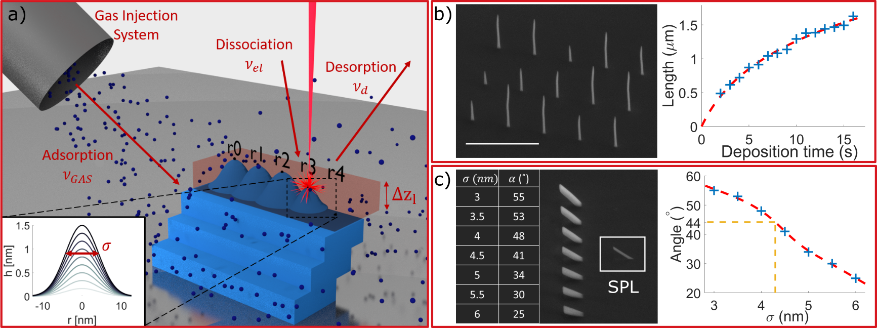
FEBID deposition is inherently a stochastic process where each electron beam dwell induces the deposition of a small number of precursor molecules. However, when averaged over the characteristic deposition times (usually in the order of a few seconds to tens of minutes), a good approximation can be achieved by describing the height of the evolving deposit as a continuous function of dwell time and radial distance from the beam center 45. Overlapping a large number of such deposits produces out of plane growth.
We develop a framework where, similar to conventional 3D printing, structures are grown via the deposition of thin slices/layers. In each layer, a series of deposits is made at beam scanning positions with dwell times , creating deposits (see Figure 1a).
Provided that the lateral separation between layers is low and that the individual deposits are small and closely spaced, the total height increment at any is the sum over all neighboring deposits. For consistent growth, this needs to be equal to the height of a layer , , resulting in a set of equations for each layer depending on the inter-point distances and dwell times:
| (1) |
where is the set of all deposits of a layer in the proximity of (referred to as neighboring points), and is the dwell time associated to each point of the layer.
In general, these equations form a non-linear optimization problem which is computationally expensive to solve. However, under the assumption that the deposit evolution can be well approximated by a separable function of time and space , we can reduce Equation 1 to a matrix equation that is numerically efficiently solvable:
| (2) |
where is a symmetric matrix, here referred to as the intra-layer proximity matrix. The dwell time values needed for consistent growth can then be calculated numerically by solving this matrix equation and inverting . This framework allows us to adjust for inter-deposit proximity effects within a layer of a 3D object, similarly to “self-consistent” dose correction algorithms employed in electron beam lithography 46, 47. Here we treat each slice of a 3D object separately, reducing the hard problem of a general 3D growth to a set of 2D consistency equations, significantly reducing the calculation complexity.
To use the above framework for the realistic modeling of a FEBID deposition, an accurate expression for is needed. In the following, we determine this function for the Langmuir FEBID model under equilibrium conditions. 45 Using the compact notation based on the characteristic FEBID frequencies that we previously developed 48, the dynamics of fractional surface molecule coverage under no diffusion can be described as a competition between the characteristic frequencies of gas adsorption (), thermal desorption () and electron-induced precursor dissociation ():
| (3) |
The corresponding growth rate () is proportional to the amount of gas present and the electron dissociation frequency:
| (4) |
Equations 3 and 4 can be solved analytically, describing the depletion of gas coverage under electron beam dissociation, and subsequent growth of the induced deposit (see Supporting Information S1.1)45.
To specify the the spatial dependence of deposits, the profile of the effective flux of electrons inducing decomposition as a function of the radial distance from the electron beam is required. For focused beams, this can be approximated by a Gaussian function21:
| (5) |
where is the effective standard deviation, and the dissociation frequency in the center of the beam.
In general, the surface coverage will evolve during the beam dwell time, converging to an equilibrium distribution on the gas dynamics time scale (see Supporting Information S1.1):
| (6) |
However, when growing either under electron limited conditions where the precursor depletion is small (), or in the case when the characteristic dwell time (usually on the order of 1ms) is much longer than the time-scale for convergence to equilibrium (), we can assume that the system is at equilibrium at all times during the growth. This simplifies the expression for to:
| (7) |
In this form, is written as a separable function with no further approximations. We follow this approach in our experiments as discussed below.
To allow for an analytical solution, in the above analysis we did not consider the effect of diffusion, which may become important in FEBID under mass-transport limited conditions. 45 However, in the context of Langmuir FEBID, the addition of diffusion would only alter the relevant timescales by speeding up the gas dynamics, as shown in Supporting Information S2. The separable form of deposit evolution could also be recovered in this case, albeit with a more complex form for the spatial part s(r).
3 Experimental determination of growth parameters
For the effective implementation of the model described above, a good approximation for needs to be determined. In the following, we focus on the standard Pt-based precursor. A generalization to other precursors is discussed later.
To apply our model experimentally, key deposition parameters need to be determined for the given experimental conditions. Although in recent years a significant effort has been made towards determining these both through experiment 49, 50, 51, 52, 21, 20 and simulations 53, 54, 55, 56, 57, the size of the parameter space still prevents confident ab-initio growth predictions. Here we demonstrate a set of experiments (Figures 1b and 1c) designed to find the minimal set of parameters which represent our growth conditions, enabling a simple calibration and preventing overfitting.
We measure the growth parameters by building a set of standardized structures, isolating the dependence of the growth rate to particular factors. Firstly, to determine growth rate at the center of the beam, a set of spot depositions is built in parallel with different total deposition times (Figure 1b). The resulting lengths of the vertical nanowires are measured and plotted against the deposition times.
Under the experimental conditions used in this paper (see Experimental), we have observed no more than 7% variation in the average growth rate when varying the dwell and refresh times used in 3D FEBID deposition (see Supporting Information S3). Therefore, we can safely assume that Equation 7 provides a good approximation of the deposition.
The sublinear dependence of nanowire length on the deposition times can thus be understood via the enhancement of thermal desorption due to beam-induced heating 55. The absolute changes in local temperature during deposition are not expected to be large compared to room temperature, being usually in the order of 10K 55, 58. We can thus expand the desorption temperature dependence to first order:
| (8) |
where is the desorption attempt frequency, is the base deposition temperature, is the change in temperature due to electron beam heating, is the desorption at , and .
The significant effect of local temperature, together with low equilibrium precursor coverage in Pt FEBID 59, implies a strong dependence of the growth rates on desorption. Therefore, even though in general we allow for the full form of the equilibrium growth rate (Equation 7) in our model, we have found that the desorption dominated regime ()48 results in the best fit to our experimental conditions.
Under the assumption that the incident beam heating rate is the same at all dwell points and that the characteristic thermal transport time scale is expected to be short relative to the dwell times55, a quasi-steady-state temperature can be assumed for every dwell. Hence, the temperature variation during deposition is fully captured by a geometrical factor , giving account for the resistance of the 3D structure to heat transport at the point of scanning ()55.
Considering the effect of beam heating in the desorption-dominated regime, Equation 7 gives a Gaussian deposit (see inset in Figure 1a):
| (9) |
where the growth rate in the center of the beam at a base deposition temperature , thermal resistance scaling factor , and the standard deviation of the deposit are parameters that need to be determined. The exponential temperature dependence for desorption (Equation 8) is expressed here through the geometry-dependent factor . For details about the implementation of the resistance model and the derivation of Equation 9 can be found in Supporting Information S4.2.
This experiment, involving vertical deposits, allows us to remove the potential influence of the geometry of the structure and proximity effects on the resulting growth. We extract the expected dependence of lengths on deposition times based on Equation 9, with as their width, and growth rate and resistance scaling factor as fitting parameters (see Supporting Information S4.3 for the full derivation):
| (10) |
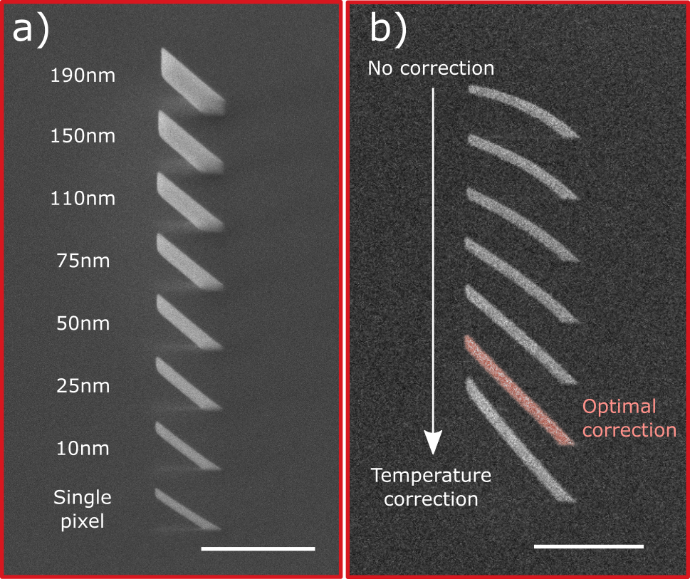
A second experiment (Figure 1c) is designed to obtain a value for . For this, a set of nominally 150nm wide straight nanowires tilted at 45∘ is built using the algorithm, while varying the value of in the model with the goal of matching the angle of a single pixel thin nanowire built with the same conditions. For the Pt precursor, we find -nms-1, and -nm, depending on the SEM system and the conditions inside the microscope chamber, such as temperature, base pressure, and precursor flux.
This two-step calibration procedure allows us to uniquely determine all growth parameters required for implementing an algorithm to pattern 3D complex structures. We further tested the validity of the calibration protocol by growing two sets of additional test structures: nanowires with constant out-of-plane angle and variable controllable width (Figure 2a), and nominally-straight nanowires, where the value obtained by the fit in Figure 1b leads to the growth of a straight structure (see "Optimal correction" in Figure 2b).
Apart from temperature, we studied other potentially-relevant effects such as electron beam defocussing and gas flux anisotropy. These have been found to have a relatively small effect for our experimental conditions, but can be important for very fine growth in certain structures and deposition regimes. If required, further corrections of this type can be easily implemented in our model at the expense of introducing additional parameters that require independent calibration (see Supporting Information S5).
4 3D printing algorithm
We have implemented the layer-by-layer growth model explained above in a three-step algorithm designed to generate beam scanning patterns for FEBID deposition of 3D arbitrary geometries. The algorithm creates deposition sequences directly from STL files that can be designed in any standard 3D CAD software, the same approach followed by standard 3D printers. This approach, in combination with the model described above, is a significant improvement with respect to recent FEBID works 43, 44, simplifying the design and enabling the fabrication of complex 3D nano-objects. In this section we give an outline of the algorithm and demonstrate its effectiveness and flexibility.
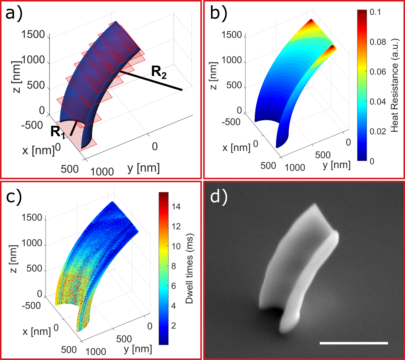
The workflow of the algorithm is described using the example of a free-standing concave surface (Figure 3a-c), with an SEM image of the fabricated nanostructure given in Figure 3d. Firstly, a geometry is defined with an STL file which is sliced using constant-z planes, defining the layers of the structure (Figure 3a). In all experiments performed here, a maximum layer height of nm is set, to guarantee that the approximation of thin layers remains valid. Additionally, an adaptive slicing procedure has been implemented, adjusting the slice thickness based on the local angle of a structure. In this way, low hanging features are more finely defined, and a low lateral displacement between layers is maintained. From each slice, a dense mesh of dwell points is created, with points separated by a lateral “pitch” distance. We set both the displacement between layers, and the pitch to be 3nm. This value has been determined from dedicated experiments (see Supporting Information S7), where single nanowires were found to be widely independent of point pitch, for pitch values below 4nm, in agreement with literature.20
In a second step, geometry-dependent factors affecting the growth are calculated, and included as growth parameters for each dwell point. Specifically, the previously discussed resistance-based model for beam-induced heating is implemented, as displayed in Figure 3b. Further corrections for second-order effects such as beam defocussing and gas flux anisotropy are also possible, but only applied to objects where the added complexity is essential for successful deposition (see Supporting Information S5). We anticipate that this second step of the algorithm could be expanded further by including additional factors relevant in other conditions and geometries, such as diffusion 55 and the dependence of secondary electron emission with local geometry. 52 These, together with the measured calibration parameters, would redefine the model for deposition, , at every dwell point.
Thirdly, we implement the per-layer dwell time solver. Inter-point distances are computed and, together with the growth model, result in the intra-layer proximity matrix . The optimization problem for finding the appropriate dwell times at each point (as per Equation 2) is then solved using a non-negative linear-least squares solver. The colormap of Figure 3c represents the resulting dwell times at each position.
Finally, the beam scanning pattern is generated out of the computed dwells. In each layer, the beam is set to make multiple passes, reversing its direction from layer to layer in a “serpentine” pattern36, to avoid exceeding a set maximum dwell time (5ms) and improving the smoothness of the deposition. The generated pattern is deposited, resulting in the SEM image shown in Figure 3d.
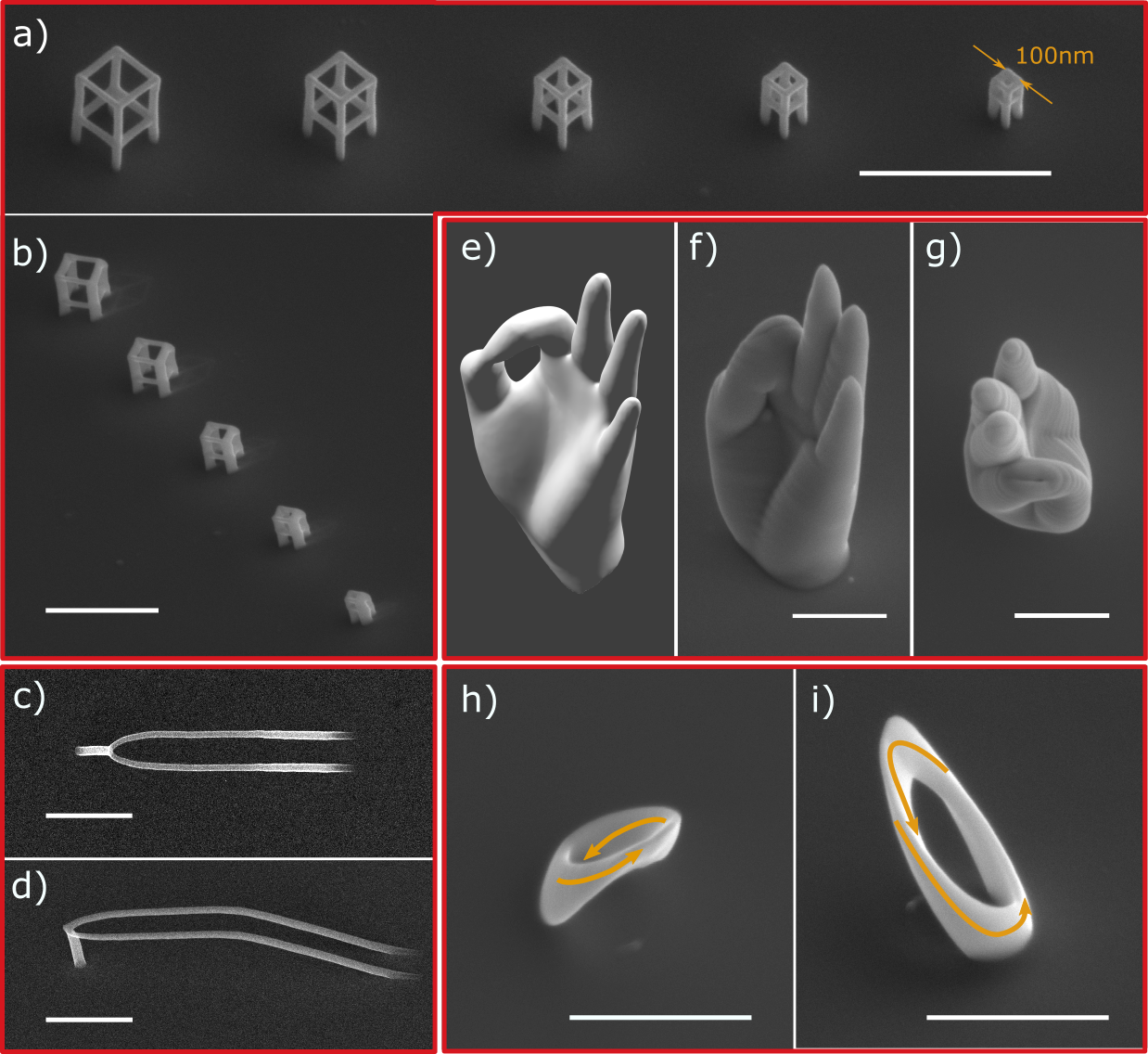
In what follows, we demonstrate the capabilities of the algorithm by patterning a range of geometries using two different (Pt- and Co-based) precursors. We first show that the fabrication of networks of straight nanowires can be reproduced, similar to the existing FEBID algorithms,43, 44 by building a sequence of nanocubes of different sizes with half-pitch down to 50nm (see Figure 4a-b and Supporting Information S8 for further details). Secondly, expanding recent achievements in nanowire device fabrication 35, 36, in Figure 4c-d we create a free-standing looped nanowire circuit formed by segments at different angles. The high quality and smoothness of the connections achieved here show the potential of our method to nano-prototype advanced 3D nanoelectronic devices. 35.
Finally, the main advantage of our approach is the capability to fabricate arbitrary three-dimensional architectures out of 3D CAD files. As an example, we have fabricated a nanoscale human hand replica (Figure 4e-g) and a Möbius strip (Figure 4h-i). These example structures present a wide range of features at different scales which are accurately replicated in experiments. In particular, Figure 4h-i shows the potential of this approach where, as far as we are aware, the smallest realization of a magnetic Möbius strip has been fabricated. See the video in Supporting Information for a full characterization of this structure at multiple angles, and comparison with the corresponding model file.
We note though, that the thickening of some features is observed for the built structure with respect to the model, e.g. the hand (Figure 4f) and the associated STL file (Figure 4e). This edge thickening effect is expected when creating a volumetric object via FEBID due to the penetration of the primary electron beam through the structure, and subsequent generation of backscattered electrons and type II secondary electrons. In order to correct for this additional precursor dissociation, a “shape-dimension adjustment technique”47 as the one employed in electron beam lithography could be implemented.
Another point to remark is that the model has been primarily developed using the standard Pt precursor due to its fast growth rate (of the order of 100nms-1), low dependence on refresh times, and a well-known mechanism for decomposition under focused electron beams60. Figure 4h-i demonstrate the algorithm’s robustness when applied to other precursors. The Co-based precursor used to build this structure has a significantly more complex chemical behavior, including autocatalytic effects 61, 62. We attribute the transferability of our algorithm to complex gases to the ability of the basic Gaussian deposit model with a constant vertical growth rate, with no temperature correction:
| (11) |
to capture the effective average of deposition and give satisfactory first-order results for most regimes. This is especially true for wide structures (as opposed to single-pixel nanowires) because scanning along their width introduces a natural refresh rate. Moreover, beam heating effects are greatly reduced due to the higher heat conductivity provided by a larger volume, leading to more consistent growth rates (see Supporting Information S4.2).
5 Conclusion
We present a framework that makes possible high-fidelity layer-by-layer growth of complex-shaped 3D nanostructures using focused electron beams. Based on a layer-by-layer growth implemented in combination with the FEBID continuum model and proximity effect corrections, we can effectively account for a variety of effects, including beam-induced heating, defocussing, and gas anisotropy. These effects have been studied for the Pt precursor, where we demonstrate how a large number of fundamental parameters can be reduced to only three, which are capable of effectively modeling the 3D deposition process.
The framework has been implemented computationally to generate beam scanning patterns from STL files created by any standard 3D CAD software. Using this approach, a wide range of nanogeometries which were until now inaccessible has been fabricated. These include surfaces with curvature along arbitrary directions, a Möbius strip and a replica of a human hand. We have successfully tested our platform in three SEM systems and using two precursors with different physical and chemical properties, thus demonstrating the robustness and applicability of the technique.
This work paves the way for the advanced nano-manufacturing of 3D objects in a wide range of nanotechnology areas, making a fundamental step towards the study of advanced effects and their future exploitation.
6 Experimental
Three different dual-beam microscope systems were used for FEBID experiments: Helios 600 at the Wolfson Electron Microscopy Suite of University of Cambridge, FEI Nova 200, and Helios 660 NanoLab at the Kelvin Nanocharacterisation Centre of University of Glasgow. Helios 600 and Nova 200 were used for deposition of \chMeCpPt(Me)3, while Helios 660 was used with \chCo2(CO)8 precursor.
All depositions were performed on p-doped Si substrates under 21pA, 30kV electron beams. The algorithm for computing dwell points and corresponding dwell times was implemented in MATLAB using the built-in Optimization Toolbox. Computation times for all structures were in the order of s on most modern desktop computers, with the exception of the hand (Figure 4e-g) which took several minutes. The algorithm was in some cases supplemented with stage tilting to build features at various angles. In particular, this was exploited for the structures on Figure 4a-b(c-d) by building at 45∘(30∘) tilt in order to realize nanowires parallel to the substrate. The fabrication times ranged from 2s for the shortest pillar in Figure 1b, 1min for the largest cube (Figure 4a-b), and up to 65min and 75min for the Möbius and hand respectively (Figure 4e-g). For more information about the access to the software used in this paper, please contact the corresponding authors.
This work was supported by the EPSRC Cambridge NanoDTC EP/L015978/1, an EPSRC Early Career Fellowship EP/M008517/1, and the Winton Program for the Physics of Suistanability. L. Skoric acknowledges support from St Johns College of the University of Cambridge. C.Donnelly was supported by the Leverhulme Trust (ECF-2018-016), the Isaac Newton Trust (18-08) and the L’Oréal-UNESCO UK and Ireland Fellowship For Women In Science. Sara Merino-Aceituno was supported by the Vienna Research Groups grant number VRG17-014 by the Vienna Science and Technology Fund. Dédalo Sanz-Hernández acknowledges a Girton College Pfeiffer Scholarship.
The authors thank the staff of the Wolfson Electron Microscopy Suite of University of Cambridge and the Kelvin Nanocharacterisation Centre of University of Glasgow for technical support. We thank Jason D. Fowlkes, A. Hierro-Rodriguez and A. Welbourne for helpful discussions.
-
•
Experimental and technical details (PDF)
-
•
Video showing the Möbius strip from different angles compared to the corresponding 3D model (AVI)
References
- Qian and Wang 2010 Qian, T.; Wang, Y. Micro/Nano-Fabrication Technologies for Cell Biology. Med Biol Eng Comput 2010, 48, 1023–1032
- Fernández-Pacheco et al. 2017 Fernández-Pacheco, A.; Streubel, R.; Fruchart, O.; Hertel, R.; Fischer, P.; Cowburn, R. P. Three-Dimensional Nanomagnetism. Nat. Commun. 2017, 8, 15756
- Kadic et al. 2019 Kadic, M.; Milton, G. W.; van Hecke, M.; Wegener, M. 3D Metamaterials. Nat Rev Phys 2019, 1, 198–210
- Vavassori et al. 2016 Vavassori, P.; Pancaldi, M.; Perez-Roldan, M. J.; Chuvilin, A.; Berger, A. Remote Magnetomechanical Nanoactuation. Small 2016, 12, 1013–1023
- Maruo et al. 1997 Maruo, S.; Nakamura, O.; Kawata, S. Three-Dimensional Microfabrication with Two-Photon-Absorbed Photopolymerization. Opt. Lett., OL 1997, 22, 132–134
- Seniutinas et al. 2018 Seniutinas, G.; Weber, A.; Padeste, C.; Sakellari, I.; Farsari, M.; David, C. Beyond 100 nm Resolution in 3D Laser Lithography — Post Processing Solutions. Microelectronic Engineering 2018, 191, 25–31
- Lewis 2006 Lewis, J. A. Direct Ink Writing of 3D Functional Materials. Advanced Functional Materials 2006, 16, 2193–2204
- Lewis et al. 2017 Lewis, B. B.; Winkler, R.; Sang, X.; Pudasaini, P. R.; Stanford, M. G.; Plank, H.; Unocic, R. R.; Fowlkes, J. D.; Rack, P. D. 3D Nanoprinting via Laser-Assisted Electron Beam Induced Deposition: Growth Kinetics, Enhanced Purity, and Electrical Resistivity. Beilstein J Nanotechnol 2017, 8, 801–812
- Takai et al. 2014 Takai, T.; Nakao, H.; Iwata, F. Three-Dimensional Microfabrication Using Local Electrophoresis Deposition and a Laser Trapping Technique. Opt. Express, OE 2014, 22, 28109–28117
- Hirt et al. 2016 Hirt, L.; Ihle, S.; Pan, Z.; Dorwling-Carter, L.; Reiser, A.; Wheeler, J. M.; Spolenak, R.; Vörös, J.; Zambelli, T. Template-Free 3D Microprinting of Metals Using a Force-Controlled Nanopipette for Layer-by-Layer Electrodeposition. Adv. Mater. 2016, 28, 2311–2315
- Momotenko et al. 2016 Momotenko, D.; Page, A.; Adobes-Vidal, M.; Unwin, P. R. Write–Read 3D Patterning with a Dual-Channel Nanopipette. ACS Nano 2016, 10, 8871–8878
- Winkler et al. 2019 Winkler, R.; Fowlkes, J. D.; Rack, P. D.; Plank, H. 3D Nanoprinting via Focused Electron Beams. Journal of Applied Physics 2019, 125, 210901
- Matsui 2012 Matsui, S. In Encyclopedia of Nanotechnology; Bhushan, B., Ed.; Springer Netherlands: Dordrecht, 2012; pp 866–876
- Esposito et al. 2015 Esposito, M.; Tasco, V.; Cuscunà, M.; Todisco, F.; Benedetti, A.; Tarantini, I.; Giorgi, M. D.; Sanvitto, D.; Passaseo, A. Nanoscale 3D Chiral Plasmonic Helices with Circular Dichroism at Visible Frequencies. ACS Photonics 2015, 2, 105–114
- Bezryadin et al. 2000 Bezryadin, A.; Lau, C. N.; Tinkham, M. Quantum Suppression of Superconductivity in Ultrathin Nanowires. Nature 2000, 404, 971
- Belkin et al. 2015 Belkin, A.; Belkin, M.; Vakaryuk, V.; Khlebnikov, S.; Bezryadin, A. Formation of Quantum Phase Slip Pairs in Superconducting Nanowires. Phys. Rev. X 2015, 5, 021023
- Zhu et al. 2018 Zhu, D.; Zhao, Q.-Y.; Choi, H.; Lu, T.-J.; Dane, A. E.; Englund, D.; Berggren, K. K. A Scalable Multi-Photon Coincidence Detector Based on Superconducting Nanowires. Nature Nanotech 2018, 13, 596–601
- Hirt et al. 2017 Hirt, L.; Reiser, A.; Spolenak, R.; Zambelli, T. Additive Manufacturing of Metal Structures at the Micrometer Scale. Advanced Materials 2017, 29, 1604211
- Jesse et al. 2016 Jesse, S.; Borisevich, A. Y.; Fowlkes, J. D.; Lupini, A. R.; Rack, P. D.; Unocic, R. R.; Sumpter, B. G.; Kalinin, S. V.; Belianinov, A.; Ovchinnikova, O. S. Directing Matter: Toward Atomic-Scale 3D Nanofabrication. ACS Nano 2016, 10, 5600–5618
- Winkler et al. 2018 Winkler, R.; Lewis, B.; Fowlkes, J.; Rack, P.; Plank, H. High-Fidelity 3D-Nanoprinting via Focused Electron Beams: Growth Fundamentals. ACS Appl. Nano Mater. 2018, 1, 1014–1027
- Utke et al. 2008 Utke, I.; Hoffmann, P.; Melngailis, J. Gas-Assisted Focused Electron Beam and Ion Beam Processing and Fabrication. J. Vac. Sci. Technol. B Microelectron. Nanometer Struct. Process. Meas. Phenom. 2008, 26, 1197–1276
- Huth et al. 2018 Huth, M.; Porrati, F.; Dobrovolskiy, O. V. Focused Electron Beam Induced Deposition Meets Materials Science. Microelectronic Engineering 2018, 185-186, 9–28
- Porrati et al. 2015 Porrati, F.; Pohlit, M.; Müller, J.; Barth, S.; Biegger, F.; Gspan, C.; Plank, H.; Huth, M. Direct Writing of CoFe Alloy Nanostructures by Focused Electron Beam Induced Deposition from a Heteronuclear Precursor. Nanotechnology 2015, 26, 475701
- Makise et al. 2014 Makise, K.; Mitsuishi, K.; Shimojo, M.; Shinozaki, B. Microstructural Analysis and Transport Properties of MoO and MoC Nanostructures Prepared by Focused Electron Beam-Induced Deposition. Sci. Rep. 2014, 4, 5740
- Winhold et al. 2014 Winhold, M.; Weirich, P. M.; Schwalb, C. H.; Huth, M. Superconductivity and Metallic Behavior in PbxCyO Structures Prepared by Focused Electron Beam Induced Deposition. Appl. Phys. Lett. 2014, 105, 162603
- Pablo-Navarro et al. 2017 Pablo-Navarro, J.; Sanz-Hernández, D.; Magén, C.; Fernández-Pacheco, A.; de Teresa, J. M. Tuning Shape, Composition and Magnetization of 3D Cobalt Nanowires Grown by Focused Electron Beam Induced Deposition (FEBID). J. Phys. D: Appl. Phys. 2017, 50, 18LT01
- Bernau et al. 2010 Bernau, L.; Gabureac, M.; Erni, R.; Utke, I. Tunable Nanosynthesis of Composite Materials by Electron-Impact Reaction. Angew. Chem. Int. Ed. 2010, 49, 8880–8884
- Ke et al. 2013 Ke, X.; Bittencourt, C.; Bals, S.; Tendeloo, G. V. Low-Dose Patterning of Platinum Nanoclusters on Carbon Nanotubes by Focused-Electron-Beam-Induced Deposition as Studied by TEM. Beilstein J. Nanotechnol. 2013, 4, 77–86
- Shawrav et al. 2016 Shawrav, M. M.; Taus, P.; Wanzenboeck, H. D.; Schinnerl, M.; Stöger-Pollach, M.; Schwarz, S.; Steiger-Thirsfeld, A.; Bertagnolli, E. Highly Conductive and Pure Gold Nanostructures Grown by Electron Beam Induced Deposition. Sci Rep 2016, 6
- Serrano-Ramón et al. 2013 Serrano-Ramón, L.; Fernández-Pacheco, A.; Córdoba, R.; Magén, C.; Rodríguez, L. A.; Petit, D.; Cowburn, R. P.; Ibarra, M. R.; Teresa, J. M. D. Improvement of Domain Wall Conduit Properties in Cobalt Nanowires by Global Gallium Irradiation. Nanotechnology 2013, 24, 345703
- Botman et al. 2006 Botman, A.; Mulders, J. J. L.; Weemaes, R.; Mentink, S. Purification of Platinum and Gold Structures after Electron-Beam-Induced Deposition. Nanotechnology 2006, 17, 3779–3785
- Botman et al. 2009 Botman, A.; Mulders, J. J. L.; Hagen, C. W. Creating Pure Nanostructures from Electron-Beam-Induced Deposition Using Purification Techniques: A Technology Perspective. Nanotechnology 2009, 20, 372001
- Winkler et al. 2017 Winkler, R.; Schmidt, F.-P.; Haselmann, U.; Fowlkes, J. D.; Lewis, B. B.; Kothleitner, G.; Rack, P. D.; Plank, H. Direct-Write 3D Nanoprinting of Plasmonic Structures. ACS Appl. Mater. Interfaces 2017, 9, 8233–8240
- Koops et al. 2001 Koops, H. W. P.; Hoinkis, O. E.; Honsberg, M. E. W.; Schmidt, R.; Blum, R.; Böttger, G.; Kuligk, A.; Liguda, C.; Eich, M. Two-Dimensional Photonic Crystals Produced by Additive Nanolithography with Electron Beam-Induced Deposition Act as Filters in the Infrared. Microelectronic Engineering 2001, 57-58, 995–1001
- Sanz-Hernández et al. 2017 Sanz-Hernández, D.; Hamans, R. F.; Liao, J.-W.; Welbourne, A.; Lavrijsen, R.; Fernández-Pacheco, A. Fabrication, Detection, and Operation of a Three-Dimensional Nanomagnetic Conduit. ACS Nano 2017, 11, 11066–11073
- Sanz-Hernández et al. 2018 Sanz-Hernández, D.; Hamans, R. F.; Osterrieth, J.; Liao, J.-W.; Skoric, L.; Fowlkes, J. D.; Rack, P. D.; Lippert, A.; Lee, S. F.; Lavrijsen, R.; Fernández-Pacheco, A. Fabrication of Scaffold-Based 3D Magnetic Nanowires for Domain Wall Applications. Nanomaterials 2018, 8, 483
- Fernández-Pacheco et al. 2009 Fernández-Pacheco, A.; Teresa, J. M. D.; Córdoba, R.; Ibarra, M. R. Magnetotransport Properties of High-Quality Cobalt Nanowires Grown by Focused-Electron-Beam-Induced Deposition. J. Phys. D: Appl. Phys. 2009, 42, 055005
- Wartelle et al. 2017 Wartelle, A.; Pablo-Navarro, J.; Staňo, M.; Bochmann, S.; Pairis, S.; Rioult, M.; Thirion, C.; Belkhou, R.; de Teresa, J. M.; Magén, C.; Fruchart, O. Transmission XMCD-PEEM Imaging of an Engineered Vertical FEBID Cobalt Nanowire with a Domain Wall. Nanotechnology 2017, 29, 045704
- Keller et al. 2018 Keller, L.; Mamoori, M. K. I. A.; Pieper, J.; Gspan, C.; Stockem, I.; Schröder, C.; Barth, S.; Winkler, R.; Plank, H.; Pohlit, M.; Müller, J.; Huth, M. Direct-Write of Free-Form Building Blocks for Artificial Magnetic 3D Lattices. Sci. Rep. 2018, 8, 6160
- Friedli and Utke 2009 Friedli, V.; Utke, I. Optimized Molecule Supply from Nozzle-Based Gas Injection Systems for Focused Electron- and Ion-Beam Induced Deposition and Etching: Simulation and Experiment. J. Phys. D: Appl. Phys. 2009, 42, 125305
- Bresin et al. 2013 Bresin, M.; Toth, M.; Dunn, K. A. Direct-Write 3D Nanolithography at Cryogenic Temperatures. Nanotechnology 2013, 24, 035301
- Riedesel et al. 2019 Riedesel, C.; Müller, I.; Kaufmann, N.; Adolf, A.; Kämmer, N.; Fritz, H.; Eberle, A. L.; Zeidler, D. First Demonstration of a 331-Beam SEM. Metrology, Inspection, and Process Control for Microlithography XXXIII. 2019; p 1095931
- Fowlkes et al. 2018 Fowlkes, J. D.; Winkler, R.; Lewis, B. B.; Fernández-Pacheco, A.; Skoric, L.; Sanz-Hernández, D.; Stanford, M. G.; Mutunga, E.; Rack, P. D.; Plank, H. High-Fidelity 3D-Nanoprinting via Focused Electron Beams: Computer-Aided Design (3BID). ACS Appl. Nano Mater. 2018, 1, 1028–1041
- Keller and Huth 2018 Keller, L.; Huth, M. Pattern Generation for Direct-Write Three-Dimensional Nanoscale Structures via Focused Electron Beam Induced Deposition. Beilstein J. Nanotechnol. 2018, 9, 2581–2598
- Toth et al. 2015 Toth, M.; Lobo, C.; Friedli, V.; Szkudlarek, A.; Utke, I. Continuum Models of Focused Electron Beam Induced Processing. Beilstein J Nanotechnol 2015, 6, 1518–1540
- Owen 1990 Owen, G. Methods for Proximity Effect Correction in Electron Lithography. J. Vac. Sci. Technol. B 1990, 8, 1889
- Parikh 1979 Parikh, M. Corrections to Proximity Effects in Electron Beam Lithography. I. Theory. Journal of Applied Physics 1979, 50, 4371–4377
- Sanz-Hernández and Fernández-Pacheco 2017 Sanz-Hernández, D.; Fernández-Pacheco, A. Modelling Focused Electron Beam Induced Deposition beyond Langmuir Adsorption. Beilstein J. Nanotechnol. 2017, 8, 2151–2161
- van Dorp et al. 2009 van Dorp, W. F.; Wnuk, J. D.; Gorham, J. M.; Fairbrother, D. H.; Madey, T. E.; Hagen, C. W. Electron Induced Dissociation of Trimethyl (Methylcyclopentadienyl) Platinum (IV): Total Cross Section as a Function of Incident Electron Energy. Journal of Applied Physics 2009, 106, 074903
- Wnuk et al. 2009 Wnuk, J. D.; Gorham, J. M.; Rosenberg, S. G.; van Dorp, W. F.; Madey, T. E.; Hagen, C. W.; Fairbrother, D. H. Electron Induced Surface Reactions of the Organometallic Precursor Trimethyl(Methylcyclopentadienyl)Platinum(IV). J. Phys. Chem. C 2009, 113, 2487–2496
- Yang et al. 2017 Yang, C.; Winkler, R.; Dukic, M.; Zhao, J.; Plank, H.; Fantner, G. E. Probing the Morphology and Evolving Dynamics of 3D Printed Nanostructures Using High-Speed Atomic Force Microscopy. ACS Appl. Mater. Interfaces 2017, 9, 24456–24461
- Fowlkes and Rack 2010 Fowlkes, J. D.; Rack, P. D. Fundamental Electron-Precursor-Solid Interactions Derived from Time-Dependent Electron-Beam-Induced Deposition Simulations and Experiments. ACS Nano 2010, 4, 1619–1629
- Smith et al. 2007 Smith, D. A.; Fowlkes, J. D.; Rack, P. D. A Nanoscale Three-Dimensional Monte Carlo Simulation of Electron-Beam-Induced Deposition with Gas Dynamics. Nanotechnology 2007, 18, 265308
- Fowlkes et al. 2016 Fowlkes, J. D.; Winkler, R.; Lewis, B. B.; Stanford, M. G.; Plank, H.; Rack, P. D. Simulation-Guided 3D Nanomanufacturing via Focused Electron Beam Induced Deposition. ACS Nano 2016, 10, 6163–6172
- Mutunga et al. 2019 Mutunga, E.; Winkler, R.; Sattelkow, J.; Rack, P. D.; Plank, H.; Fowlkes, J. D. Impact of Electron-Beam Heating during 3D Nanoprinting. ACS Nano 2019, 13, 5198–5213
- Sushko et al. 2016 Sushko, G. B.; Solov’yov, I. A.; Solov’yov, A. V. Molecular Dynamics for Irradiation Driven Chemistry: Application to the FEBID Process*. Eur. Phys. J. D 2016, 70, 217
- Shen et al. 2012 Shen, J.; Muthukumar, K.; Jeschke, H. O.; Valentí, R. Physisorption of an Organometallic Platinum Complex on Silica: Anab Initiostudy. New J. Phys. 2012, 14, 073040
- Bouscaud et al. 2012 Bouscaud, D.; Pesci, R.; Berveiller, S.; Patoor, E. Estimation of the Electron Beam-Induced Specimen Heating and the Emitted X-Rays Spatial Resolution by Kossel Microdiffraction in a Scanning Electron Microscope. Ultramicroscopy 2012, 115, 115–119
- Friedli et al. 2007 Friedli, V.; Santschi, C.; Michler, J.; Hoffmann, P.; Utke, I. Mass Sensor for in Situ Monitoring of Focused Ion and Electron Beam Induced Processes. Appl. Phys. Lett. 2007, 90, 053106
- Wnuk et al. 2011 Wnuk, J. D.; Rosenberg, S. G.; Gorham, J. M.; van Dorp, W. F.; Hagen, C. W.; Fairbrother, D. H. Electron Beam Deposition for Nanofabrication: Insights from Surface Science. Surface Science 2011, 605, 257–266
- Bishop 2019 Bishop, J. D. Fundamental Advances in Focused Electron Beam Induced Processing. Thesis, University of Technology Sydney, 2019
- Muthukumar et al. 2012 Muthukumar, K.; Jeschke, H. O.; Valentí, R.; Begun, E.; Schwenk, J.; Porrati, F.; Huth, M. Spontaneous Dissociation of Co2(CO)8 and Autocatalytic Growth of Co on SiO2: A Combined Experimental and Theoretical Investigation. Beilstein J. Nanotechnol. 2012, 3, 546–555