Filtering the photoluminescence spectra of atomically thin semiconductors with graphene
Abstract
Atomically thin semiconductors made from transition metal dichalcogenides (TMDs) are model systems for investigations of strong light-matter interactions and applications in nanophotonics, opto-electronics and valley-tronics. However, the photoluminescence spectra of TMD monolayers display a large number of features that are particularly challenging to decipher. On a practical level, monochromatic TMD-based emitters would be beneficial for low-dimensional devices but this challenge is yet to be resolved. Here, we show that graphene, directly stacked onto TMD monolayers enables single and narrow-line photoluminescence arising solely from TMD neutral excitons. This filtering effect stems from complete neutralization of the TMD by graphene combined with selective non-radiative transfer of long-lived excitonic species to graphene. Our approach is applied to four tungsten and molybdenum-based TMDs and establishes TMD/graphene heterostructures as a unique set of opto-electronic building blocks, suitable for electroluminescent systems emitting visible and near-infrared photons at near THz rate with linewidths approaching the lifetime limit.
TMD monolayers (thereafter simply denoted TMD), such as MoS2, MoSe2, WS2, WSe2 are direct-bandgap semiconductors Mak et al. (2010); Splendiani et al. (2010), featuring short Bohr radii, large exciton binding energy of hundreds of meV Wang et al. (2018); Goryca et al. (2019) and picosecond excitonic radiative lifetimes at low temperature Palummo et al. (2015); Robert et al. (2016); Fang et al. (2019), all arising from their strong 2D Coulomb interactions, reduced dielectric screening and large effective masses Wang et al. (2018); Goryca et al. (2019). Since the first investigations of light emission from TMDs, it has been clear that their low-temperature spectra is composed of at least two prominent features, stemming from bright neutral excitons () and charged excitons (trions, ) Mak et al. (2013); Ross et al. (2013); Courtade et al. (2017) endowed with a binding energy of typically 20 to 40 meV relative to . Among the vast family of TMDs, one may distinguish between so-called dark and bright materials Echeverry et al. (2016). In the case of Tungsten-based TMDs, a spin-dark state lies lower than . Conversely, in Molybdenum based-TMDs, lies below (MoSe2) or very near (MoS2) the spin-dark state, resulting in brighter emission at low temperature. As a result, and emission dominate the PL spectrum of Mo-based TMDs Ross et al. (2013), whereas the emission spectra of W-based TMDs display a complex series of lines stemming from , bi-excitons ()Barbone et al. (2018); Ye et al. (2018); Paur et al. (2019); Li et al. (2018), charged excitonic states (including Courtade et al. (2017); Vaclavkova et al. (2018) and charged biexcitons () Barbone et al. (2018); Ye et al. (2018); Paur et al. (2019); Li et al. (2018)), spin-dark excitons Robert et al. (2017); Zhou et al. (2017); Zhang et al. (2017), defect-induced emission and exciton-phonon sidebands Lindlau et al. (2018); Liu et al. (2019).
Considerable progress has been made to deterministically observe intrinsic TMD emission features. In particular, encapsulation of TMDs in hexagonal boron nitride (BN) films results in narrower neutral exciton linewidth Cadiz et al. (2017); Ajayi et al. (2017), approaching the radiative limit Fang et al. (2019); Scuri et al. (2018); Back et al. (2018), without however, getting rid of the other emission features mentioned above. Even in electrostatically gated devices tuned near the charge neutrality point, sizeable emission sidebands remain observable at energies close to the feature, suggesting residual charge inhomogeneity Courtade et al. (2017); Ross et al. (2013) or intrinsic contributions from longer-lived exciton-phonon replicas Lindlau et al. (2018); Liu et al. (2019).
The complex emission spectra of TMD stimulate lively scientific debates. Conversely, obtaining atomically-thin semiconductors with single, narrow emission lines remains an important challenge in the field. An appealing solution could consist in interfacing a TMD monolayer with graphene. Indeed, the semi-metallic character of graphene and its highly symmetric electronic structure Castro Neto et al. (2009), with its Dirac point lying within the bandgap of Mo- and W- based TMD Wilson et al. (2017), makes it an ideal electron and hole acceptor, through static charge transfer Hill et al. (2017); Froehlicher et al. (2018). Unfortunately, at room temperature, the effective lifetime is in the ns range Palummo et al. (2015); Robert et al. (2016); Froehlicher et al. (2018) and interlayer coupling between TMDs and graphene results in significant PL quenching He et al. (2014); Yuan et al. (2018); Froehlicher et al. (2018) due to picosecond energy transfer mediated by either charge tunneling (Dexter-type) or longer-range dipole-dipole interaction (Förster-type) Froehlicher et al. (2018); Selig et al. (2019); Basko et al. (1999). However, a much more favorable situation may occur at lower temperatures (typically, below 100 K), where the radiative lifetime of drastically shortens Robert et al. (2016); Palummo et al. (2015) and becomes of the same order of magnitude as the theoretically estimated energy transfer time Selig et al. (2019).
In this work, we demonstrate that W- and Mo-based TMDs coupled to a graphene monolayer exhibit only one single and narrow emission line that is assigned to radiative recombination, indicating complete neutrality. The short-lived states are minimally affected by non-radiative transfer to graphene and subsequent PL quenching, in stark contrast with longer-lived excitonic species, which are massively quenched. Graphene has been recognised as a partner material of choice to improve the opto-electronic response of TMDs Massicotte et al. (2016), whereas TMDs hold promise to improve spin transport in graphene Luo et al. (2017); Avsar et al. (2017). Our results now establish TMD/graphene heterostructures as an outstanding light-emitting system readily interfaced with a quasi-transparent conductive channel.
Bright, single-line emission in TMD/graphene heterostructures
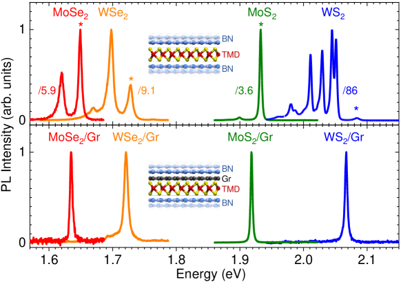
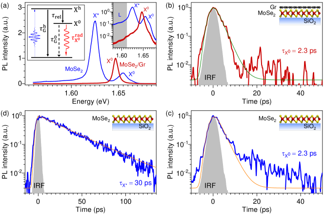
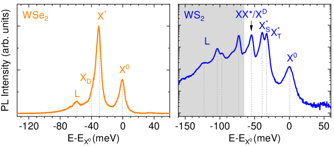
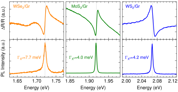
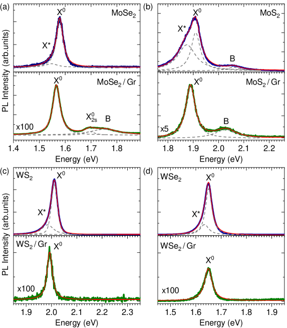
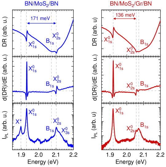
Figure 1 shows the PL spectra of van der Waals heterostructures made from monolayers of MoS2, MoSe2, WS2 and WSe2 stacked onto graphene monolayers and encapsulated in BN (lower panel). These spectra are compared to those of neighbouring BN-capped TMD regions (upper panel). All TMD/graphene spectra display one single and narrow Lorentzian emission line, with a full width at half maximum (FWHM) of typically 5 meV, suggesting minimal dephasing and disorder (see supplementary Section 1 for the fitting parameters and Section 2 for MoSe2/graphene samples with PL linewidths approaching the lieftime limit). The TMD references also display narrow emission features assigned to (see asterisks in Fig. 1, upper panel), but the latter are accompanied with the lower energy emission lines introduced above Cadiz et al. (2017); Wang et al. (2018); Vaclavkova et al. (2018); Liu et al. (2019) (see supplementary Section 3 for their assignments). The sharp PL lines in TMD/graphene are slightly redshifted (by ) with respect to in the TMD references. By measuring the temperature dependent PL spectra and the differential reflectance (DR) spectra of TMD and TMD/graphene, we can unambiguously assign these single lines to (see Fig. 2 and supplementary Section 4). Therefore, we conclude (i) that no emission is measured in TMD/graphene and (ii) that the redshift in TMD/graphene arises from dielectric screening Raja et al. (2017); Froehlicher et al. (2018). Crucially, we note that PL quenching of the line is moderate, systematically of less than one order of magnitude in all samples under study (see Fig. 1 and supplementary Section 1). The difference between PL from TMD and TMD/graphene heterostructures is particularly striking in the case of tungsten-based TMDs. In these dark materials, hot luminescence from is quite inefficient and lower lying emission lines dominate the PL spectra, especially in WS2, (see Fig. 1 and supplementary Section 3). As discussed below, all these features are much longer lived than in TMD Lagarde et al. (2014); Robert et al. (2016, 2017); Nagler et al. (2018) and are thus literally washed out in the emission spectra of TMD/graphene heterostructures due to fast non-radiative transfer to graphene.
Complete TMD neutralization
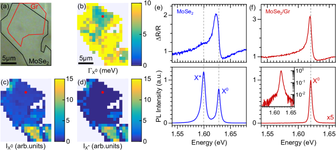
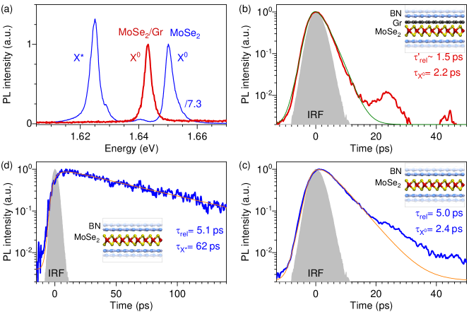
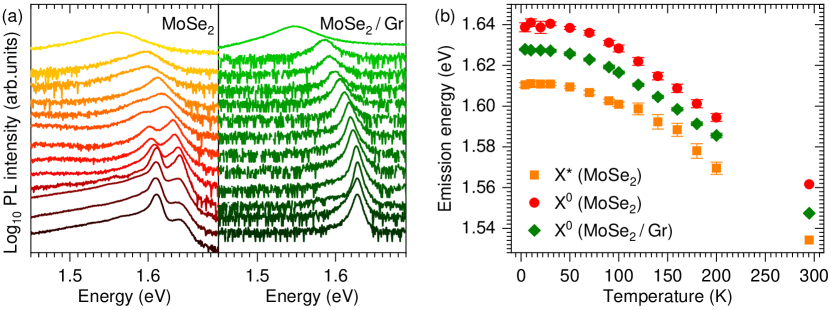
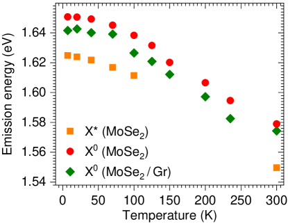
We now focus on the case of MoSe2/graphene heterostructures, with PL mapping, as well as typical DR and PL spectra shown in Fig. 2 for a BN-capped sample deposited onto a glass coverslip. The PL spectrum of BN-capped MoSe2 is composed of two lines with similar intensities, shifted by 28 meV. The high and low-energy line are assigned to and PL Ross et al. (2013), respectively. An absorption feature emerges on the DR spectrum, with an amplitude considerably smaller than that of the DR feature (Fig. 2e). In contrast, the BN-capped MoSe2/graphene region of the sample displays only absorption and emission features. As shown in Fig. 2b-d, these observations can be consistently made over the whole () area of a coupled MoSe2/graphene region. This is an important point, since TMD-based van der Waals heterostructures are known to be spatially inhomogeneous and hence, the observation of “trion-free” spectra might be accidental. In return, the absence of emission can be exploited as a reliable probe of the coupling between TMD and graphene.
We assign the absence of absorption and emission features in TMD/graphene to the transfer of all the native dopants in the TMD (either electrons or holes, with a typical density on the order of ) to graphene. Such static charge transfer leads to a slight increase of the Fermi level of graphene (typically by less than 100 meV) and to the observation of intrinsic absorption and emission. Alternate scenarii, involving residual doping in the TMD but massive quenching of formation and/or radiative recombination can safely be ruled out (see supplementary Section 5.1). TMD neutralization is corroborated by room temperature Raman scattering Froehlicher et al. (2018) and PL measurements (see supplementary Section 5.2).
Photostability and dielectric screening
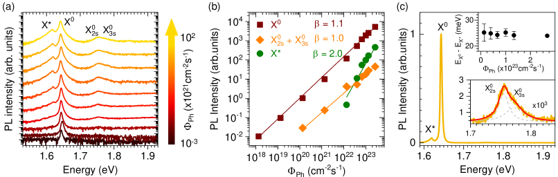
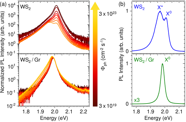
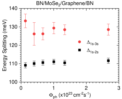
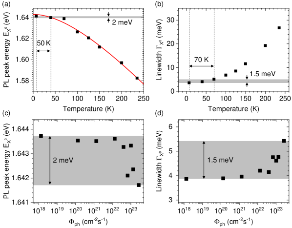
To further establish the benefits of coupling TMD to graphene, we show, in Fig. 3, the PL spectra of the BN-capped MoSe2/graphene introduced in Fig. 2 recorded under continuous wave (cw) photon fluxes (hereafter denoted ) at 2.33 eV, spanning more than five orders of magnitude, from to , i.e., . Assuming an absorptance of at 2.33 eV Li et al. (2014) and an excitonic lifetime of 2 ps in BN-capped MoSe2/graphene (see Fig. 4,5), we may estimate injected hot exciton densities ranging from up to . The PL intensity scales quasi-linearly with . We note, however, the emergence of two faint PL features. The first one is asymmetric, blueshifted by about 120 meV from and its intensity scales linearly with . We assign this feature to hot luminescence from the neutral excited excitons (at and excitons (at ). The exciton binding energy is in BN-capped MoSe2, with . Assuming for simplicity that scales proportionally to , we estimate that the presence of a graphene layer reduces down to (see supplementary Section 6). The second feature is redshifted by about , i.e., a few meV less than the line in MoSe2 (see Fig. 2c) and its intensity rises quadratically with . Therefore, this feature could tentatively be assigned to a biexciton (). However, have recently been observed in MoSe2 Hao et al. (2017) and WSe2 Barbone et al. (2018); Ye et al. (2018); Paur et al. (2019); Li et al. (2018) monolayers and display binding energies of , significantly lower than the value observed here in a system that undergoes more screening due to the presence of graphene. Thus, the lower energy feature is tentatively assigned to emission from photocreated trions with a slightly reduced binding energy. As previously reported in other low-dimensional materials (e.g.; carbon nanotubes Yuma et al. (2013)), at sufficiently large exciton densities, bimolecular exciton-exciton annihilation (EEA Mouri et al. (2014)) can create free carriers. Subsequent photon absorption leads to formation and emission. In this scenario, a quadratic scaling with is expected. Noteworthy, emission remains more than one order of magnitude brighter than emission at the highest employed here, which justifies why we do not observe a sub-linear rise of the PL intensity due to EEA. The data in Fig. 3 also reveals the outstanding photostability of TMD/graphene systems that can sustain photon fluxes above typical PL non-linearity and damage thresholds in bare TMD Cadiz et al. (2016), without significant photo-induced heating (see supplementary Sections 5 and 7).
Exciton dynamics and exciton transfer time
Let us finally consider exciton dynamics in TMD/graphene. Fig. 4 compares the time-resolved PL (TRPL) of MoSe2 and MoSe2/graphene, recorded at 14 K on another sample deposited on SiO2 and excited below the state. As shown in Fig. 4a, the filtering effect evidenced in BN-capped TMD/graphene (Fig. 1) also appears prominently samples supported by a rougher SiO2 substrate (see also supplementary Section 2). A three-level system Fang et al. (2019) considering hot excitons , such as finite momentum 1s and possibly 2s excitons, formed shortly after laser excitation Steinleitner et al. (2017), (i.e., cold 1s excitons with center of mass momentum within the light cone) and the ground state is shown in the inset of Fig. 4a. As the PL rise time lies below our time resolution for all measurements on this sample, the TRPL traces in Fig. 4 are simply fit by the convolution of the instrument response function (IRF) with an exponential decay. In keeping with previous reports, the exciton lifetime () is only in bare MoSe2, and can be assigned to the radiative lifetime Robert et al. (2016), whereas display a much longer lifetime . Remarkably, within experimental accuracy, has identical values in MoSe2/graphene and in the neighbouring MoSe2 region. This striking result suggests that , the non-radiative transfer time of cold excitons () to graphene, is longer than 2 ps. Let us note, that scales as and is thus expected to be longer in MoSe2/graphene than in the nearby MoSe2 reference. Hence, observing similar in Fig. 4b,c may be coincidental and result from the compensation between the increase of in MoSe2/graphene and non-radiative transfer of to graphene with an estimated timescale (see supplementary Section 8.1). As a result, the emission yield (defined here as the number of emitted photons divided by the number of cold ) that is near unity in the bare MoSe2 monolayer Fang et al. (2019) remains high, near in MoSe2/graphene (see supplementary Section 8.2).
Still, while the integrated PL intensity from in MoSe2/graphene on SiO2 is nearly twice that of a close-lying MoSe2 reference (see Fig. 4a), the total PL intensity from MoSe2 remains times larger than that of MoSe2/graphene. Following generation of , one may form , and localised excitons (e.g., near defects) in bare MoSe2. Localised excitons contribute a low-energy tail to the PL spectra, as shown in Fig. 4a (shaded area under the blue trace). Conversely, only and localised excitons can be formed in neutral graphene/MoSe2/SiO2, which is consitent with the observed enhancement of emission. Since localised excitons have long lifetimes Lagarde et al. (2014), their emission is quenched by graphene, as evidenced in Fig. 4a (red trace). The sizeable quenching of the total PL intensity can tentatively be assigned to fast transfer of to graphene on a time scale (see inset in Fig. 4a) that is shorter than , the relaxation time of down to the light cone. This scenario is consistent with the fact that the Förster-type energy transfer time of TMD excitons to graphene is expected to be maximal for zero momentum excitons (i.e., here ) and to decrease with exciton momentum Basko et al. (1999); Selig et al. (2019). All in all, our results strongly suggest that graphene open up efficient non-radiative decay pathways that moderately quench radiative recombination but instead significantly inhibit formation. Along these lines, we expect that formation should be more efficiently inhibited in BN-capped samples, where is much longer than in SiO2 supported samples and can be experimentally resolved Fang et al. (2019).
Efficient hot exciton transfer to graphene
In Fig. 5, we investigate exciton dynamics the BN-capped sample discussed in Fig. 1-3, following pulsed optical excitation slightly below the exciton energy. Importantly, this sample is deposited on a glass coverslip and therefore immune from the cavity effects discussed in ref. Fang et al. (2019). As introduced in Fig. 1-3, PL is quenched in MoSe2/graphene, in contrast with the case of the SiO2 supported sample, where PL enhancement is observed (Fig. 4a). This difference readily suggests that formation is more efficiently quenched in BN-capped TMD/graphene. The TRPL traces are fit by solving the rate equations associated with the three-level system introduced in Fig. 4a, with two characteristic times for relaxation towards (or ) formation and (or ) decay, respectively. The short and long times correspond to the rise and decay times in the TRPL measurement, respectively Fang et al. (2019). Fig. 5b,c reveals that the PL rise time () is too close to our resolution limit to be accurately resolved in BN-capped MoSe2/graphene and is in the BN-capped MoSe2 reference. The PL decay times are in MoSe2/graphene and in the MoSe2 reference region, respectively. Interestingly, the PL rise time of the long-lived feature in BN-capped MoSe2 is closely matching the decay time. We therefore assign this time to , the relaxation time of down to the and states in BN-capped MoSe2. Hot exciton transfer results in a shortened relaxation time in BN-capped MoSe2/graphene. Finally, the lifetimes in BN-capped MoSe2 and MoSe2/graphene are assigned to the rise and decay time of their respective TRPL traces and are nearly identical ( and , respectively). With these values, following the same reasoning as for the SiO2-supported MoSe2/graphene sample discussed in Fig. 4, we can estimate that the emission yield is also near (see supplementary Section 8.2), demonstrating that non-radiative transfer has similar efficiencies in BN-capped and SiO2-supported MoSe2/graphene heterostructures. We conclude that a significant part of PL quenching is due to efficient non-radiative transfer of enabled by graphene and that PL quenching is more efficient in BN-capped Mose2/graphene than SiO2/MoSe2/graphene due to slower relaxation (or equivalently formation) in BN-capped MoSe2.
Conclusions and outlook
In closing, we have shown that graphene neutralizes atomically-thin TMDs, leading to the absence of light emission from charged excitonic species. Graphene also enables picosecond non-radiative transfer of TMD excitonic species. Starting from a given initial density, transfer of to graphene will reduce the maximum achievable density of and of other longer lived neutral excitonic compounds. The latter will be strongly quenched by graphene, whereas the former will be minimally affected owing to their picosecond radiative lifetime. As a result, exclusively contribute to the PL spectra of TMD/graphene heterostructures. The measured PL intensity is largely determined by the competition between formation and non-radiative transfer to graphene rather than by the trade-off between radiative recombination and non-radiative transfer to graphene.
Graphene is here introduced as narrow-line filter that is naturally tuned to a broad range of emitted photon energies spanning the mid-infrared to the ultraviolet regions. Our two-dimensional design naturally outperforms alternate solutions based on spectrally narrow interference filter that are considerably bulkier and lack tunability (see supplementary Section 9). Going further, high-speed (up to ), photonic and opto-electronic devices with one single bright and nearly lifetime-limited emission line (see supplementary Section 2) can be envisioned using TMD/graphene heterostructures. Such devices may also benefit from the excellent electrical contact, photodetection Massicotte et al. (2016); Arp et al. (2019), electron and spin transport Luo et al. (2017); Avsar et al. (2017) capabilities offered by TMD/graphene heterostructures. One may also foresee progress in cavity quantum electrodynamics Schneider et al. (2018), chiral optics Chervy et al. (2018) and opto-valleytronics Mak et al. (2018) by jointly exploiting the simple emission spectra of TMD/graphene heterostructures and their record-high degrees of valley coherence and valley polarization of up to 60 and 50 , respectively Lorchat et al. (2018).
Acknowledgements
The authors thank D. Basko, T. Galvani, L. Wirtz, G. Schull, S. Azzini, T. Chervy, C. Genet, M.A. Semina and M.M. Glazov for fruitful discussions. We are grateful to H. Majjad and M. Rastei for help with AFM measurements, to M. Romeo, F. Chevrier, M. Acosta, A. Boulard and the StNano clean room staff for technical support. We acknowledge financial support from the Agence Nationale de la Recherche (under grants H2DH ANR-15-CE24-0016, 2D-POEM ANR-18-ERC1-0009, D-vdW-Spin, VallEx, and MagicValley), from the LabEx NIE (Under Grant ANR-11-LABX-0058-NIE) and from the EUR NanoX (under grant VWspin and MILO).
Competing interests
The authors declare no competing interests.
Author contributions
S.B. conceived and lead the project, with C.R., D.L. and X.M. supervising the time-resolved PL measurements. E.L. and L.E.P.L. fabricated the samples. E.L., L.E.P.L., C.R., D.L. and S.B. carried out the measurements. E.L., L.E.P.L. and S.B. analysed the data with input from G.F., C.R., D.L. and X.M. T.T. and K.W. provided high-quality hexagonal BN crystals. S.B. wrote the manuscript with input from X.M., C.R., E.L. and L.E.P.L.
Methods
Our model system is a van der Waals heterostructure formed by stacking a monolayer of graphene onto a TMD monolayer using standard methods as in ref. Castellanos-Gomez et al. (2014); Zomer et al. (2014). In this work, we have investigated MoSe2, MoS2, WSe2 and WS2-based heterostructures encapsulated in hexagonal boron nitride (BN, see Fig. 1- 3 and Fig. 5) or directly deposited on SiO2 substrates (Fig. 4). All materials were mechanically exfoliated from bulk crystals. Graphene and TMD monolayers were unambiguously identified using room-temperature Raman and PL spectroscopies, respectively. Our samples were investigated at variable temperature (4 K – 300 K) by means of micro-PL and differential reflectance (DR) spectroscopy using home-built setups. Time-resolved PL measurements were performed on MoSe2-based samples, using a Ti:Sa oscillator delivering pulses with a repetition rate of 80 MHz and a synchro-scan streak camera with a temporal resolution of . All comparisons between results obtained on TMD and on TMD/graphene are based on measurements performed in the same experimental conditions on a same TMD flake partially covered with graphene (see for example Fig. 2).
References
- Mak et al. (2010) Kin Fai Mak, Changgu Lee, James Hone, Jie Shan, and Tony F. Heinz, “Atomically Thin : A New Direct-Gap Semiconductor,” Phys. Rev. Lett. 105, 136805 (2010).
- Splendiani et al. (2010) Andrea Splendiani, Liang Sun, Yuanbo Zhang, Tianshu Li, Jonghwan Kim, Chi-Yung Chim, Giulia Galli, and Feng Wang, “Emerging Photoluminescence in Monolayer ,” Nano Lett. 10, 1271–1275 (2010).
- Wang et al. (2018) Gang Wang, Alexey Chernikov, Mikhail M. Glazov, Tony F. Heinz, Xavier Marie, Thierry Amand, and Bernhard Urbaszek, “Colloquium: Excitons in atomically thin transition metal dichalcogenides,” Rev. Mod. Phys. 90, 021001 (2018).
- Goryca et al. (2019) M. Goryca, J. Li, A. V. Stier, T. Taniguchi, K. Watanabe, E. Courtade, S. Shree, C. Robert, B. Urbaszek, X. Marie, and S. A. Crooker, “Revealing exciton masses and dielectric properties of monolayer semiconductors with high magnetic fields,” Nat. Commun. 10, 4172 (2019).
- Palummo et al. (2015) Maurizia Palummo, Marco Bernardi, and Jeffrey C Grossman, “Exciton radiative lifetimes in two-dimensional transition metal dichalcogenides,” Nano Lett. 15, 2794–2800 (2015).
- Robert et al. (2016) C. Robert, D. Lagarde, F. Cadiz, G. Wang, B. Lassagne, T. Amand, A. Balocchi, P. Renucci, S. Tongay, B. Urbaszek, and X. Marie, “Exciton radiative lifetime in transition metal dichalcogenide monolayers,” Phys. Rev. B 93, 205423 (2016).
- Fang et al. (2019) H. H. Fang, B. Han, C. Robert, M. A. Semina, D. Lagarde, E. Courtade, T. Taniguchi, K. Watanabe, T. Amand, B. Urbaszek, M. M. Glazov, and X. Marie, “Control of the exciton radiative lifetime in van der waals heterostructures,” Phys. Rev. Lett. 123, 067401 (2019).
- Mak et al. (2013) Kin Fai Mak, Keliang He, Changgu Lee, Gwan Hyoung Lee, James Hone, Tony F Heinz, and Jie Shan, “Tightly bound trions in monolayer mos2,” Nat. Mater. 12, 207–211 (2013).
- Ross et al. (2013) Jason S Ross, Sanfeng Wu, Hongyi Yu, Nirmal J Ghimire, Aaron M Jones, Grant Aivazian, Jiaqiang Yan, David G Mandrus, Di Xiao, Wang Yao, et al., “Electrical control of neutral and charged excitons in a monolayer semiconductor,” Nat. Commun. 4, 1474 (2013).
- Courtade et al. (2017) E. Courtade, M. Semina, M. Manca, M. M. Glazov, C. Robert, F. Cadiz, G. Wang, T. Taniguchi, K. Watanabe, M. Pierre, W. Escoffier, E. L. Ivchenko, P. Renucci, X. Marie, T. Amand, and B. Urbaszek, “Charged excitons in monolayer WSe2: Experiment and theory,” Phys. Rev. B 96, 085302 (2017).
- Echeverry et al. (2016) J. P. Echeverry, B. Urbaszek, T. Amand, X. Marie, and I. C. Gerber, “Splitting between bright and dark excitons in transition metal dichalcogenide monolayers,” Phys. Rev. B 93, 121107 (2016).
- Barbone et al. (2018) Matteo Barbone, Alejandro R-P Montblanch, Dhiren M Kara, Carmen Palacios-Berraquero, Alisson R Cadore, Domenico De Fazio, Benjamin Pingault, Elaheh Mostaani, Han Li, Bin Chen, et al., “Charge-tuneable biexciton complexes in monolayer WSe2,” Nat. Commun. 9, 3721 (2018).
- Ye et al. (2018) Ziliang Ye, Lutz Waldecker, Eric Yue Ma, Daniel Rhodes, Abhinandan Antony, Bumho Kim, Xiao-Xiao Zhang, Minda Deng, Yuxuan Jiang, Zhengguang Lu, et al., “Efficient generation of neutral and charged biexcitons in encapsulated wse 2 monolayers,” Nat. Commun. 9, 3718 (2018).
- Paur et al. (2019) Matthias Paur, Aday J. Molina-Mendoza, Rudolf Bratschitsch, Kenji Watanabe, Takashi Taniguchi, and Thomas Mueller, “Electroluminescence from multi-particle exciton complexes in transition metal dichalcogenide semiconductors,” Nat. Commun. 10, 1709 (2019).
- Li et al. (2018) Zhipeng Li, Tianmeng Wang, Zhengguang Lu, Chenhao Jin, Yanwen Chen, Yuze Meng, Zhen Lian, Takashi Taniguchi, Kenji Watanabe, Shengbai Zhang, Dmitry Smirnov, and Su-Fei Shi, “Revealing the biexciton and trion-exciton complexes in bn encapsulatedWSe2,” Nat. Commun. 9, 3719 (2018).
- Vaclavkova et al. (2018) D Vaclavkova, J Wyzula, K Nogajewski, M Bartos, A O Slobodeniuk, C Faugeras, M Potemski, and M R Molas, “Singlet and triplet trions in WS2 monolayer encapsulated in hexagonal boron nitride,” Nanotechnology 29, 325705 (2018).
- Robert et al. (2017) C. Robert, T. Amand, F. Cadiz, D. Lagarde, E. Courtade, M. Manca, T. Taniguchi, K. Watanabe, B. Urbaszek, and X. Marie, “Fine structure and lifetime of dark excitons in transition metal dichalcogenide monolayers,” Phys. Rev. B 96, 155423 (2017).
- Zhou et al. (2017) You Zhou, Giovanni Scuri, Dominik S Wild, Alexander A High, Alan Dibos, Luis A Jauregui, Chi Shu, Kristiaan De Greve, Kateryna Pistunova, Andrew Y Joe, et al., “Probing dark excitons in atomically thin semiconductors via near-field coupling to surface plasmon polaritons,” Nat. Nanotechnol. 12, 856 (2017).
- Zhang et al. (2017) Xiao-Xiao Zhang, Ting Cao, Zhengguang Lu, Yu-Chuan Lin, Fan Zhang, Ying Wang, Zhiqiang Li, James C Hone, Joshua A Robinson, Dmitry Smirnov, et al., “Magnetic brightening and control of dark excitons in monolayer WSe2,” Nat. Nanotechnol. 12, 883 (2017).
- Lindlau et al. (2018) Jessica Lindlau, Malte Selig, Andre Neumann, Léo Colombier, Jonathan Förste, Victor Funk, Michael Förg, Jonghwan Kim, Gunnar Berghäuser, Takashi Taniguchi, et al., “The role of momentum-dark excitons in the elementary optical response of bilayer wse 2,” Nat. Commun. 9, 2586 (2018).
- Liu et al. (2019) Erfu Liu, Jeremiah van Baren, Takashi Taniguchi, Kenji Watanabe, Yia-Chung Chang, and Chun Hung Lui, “Valley-selective chiral phonon replicas of dark excitons and trions in monolayer ,” Phys. Rev. Research 1, 032007 (2019).
- Cadiz et al. (2017) F. Cadiz, E. Courtade, C. Robert, G. Wang, Y. Shen, H. Cai, T. Taniguchi, K. Watanabe, H. Carrere, D. Lagarde, M. Manca, T. Amand, P. Renucci, S. Tongay, X. Marie, and B. Urbaszek, “Excitonic linewidth approaching the homogeneous limit in MoS2-based van der waals heterostructures,” Phys. Rev. X 7, 021026 (2017).
- Ajayi et al. (2017) Obafunso A Ajayi, Jenny V Ardelean, Gabriella D Shepard, Jue Wang, Abhinandan Antony, Takeshi Taniguchi, Kenji Watanabe, Tony F Heinz, Stefan Strauf, X-Y Zhu, and James C Hone, “Approaching the intrinsic photoluminescence linewidth in transition metal dichalcogenide monolayers,” 2D Materials 4, 031011 (2017).
- Scuri et al. (2018) Giovanni Scuri, You Zhou, Alexander A. High, Dominik S. Wild, Chi Shu, Kristiaan De Greve, Luis A. Jauregui, Takashi Taniguchi, Kenji Watanabe, Philip Kim, Mikhail D. Lukin, and Hongkun Park, “Large excitonic reflectivity of monolayer encapsulated in hexagonal boron nitride,” Phys. Rev. Lett. 120, 037402 (2018).
- Back et al. (2018) Patrick Back, Sina Zeytinoglu, Aroosa Ijaz, Martin Kroner, and Atac Imamoğlu, “Realization of an electrically tunable narrow-bandwidth atomically thin mirror using monolayer ,” Phys. Rev. Lett. 120, 037401 (2018).
- Castro Neto et al. (2009) A. H. Castro Neto, F. Guinea, N. M. R. Peres, K. S. Novoselov, and A. K. Geim, “The electronic properties of graphene,” Rev. Mod. Phys. 81, 109–162 (2009).
- Wilson et al. (2017) Neil R. Wilson, Paul V. Nguyen, Kyle Seyler, Pasqual Rivera, Alexander J. Marsden, Zachary P. L. Laker, Gabriel C. Constantinescu, Viktor Kandyba, Alexei Barinov, Nicholas D. M. Hine, Xiaodong Xu, and David H. Cobden, “Determination of band offsets, hybridization, and exciton binding in 2D semiconductor heterostructures,” Science Advances 3 (2017).
- Hill et al. (2017) Heather M. Hill, Albert F. Rigosi, Archana Raja, Alexey Chernikov, Cyrielle Roquelet, and Tony F. Heinz, “Exciton broadening in WS2/graphene heterostructures,” Phys. Rev. B 96, 205401 (2017).
- Froehlicher et al. (2018) Guillaume Froehlicher, Etienne Lorchat, and Stéphane Berciaud, “Charge versus energy transfer in atomically thin graphene-transition metal dichalcogenide van der waals heterostructures,” Phys. Rev. X 8, 011007 (2018).
- He et al. (2014) Jiaqi He, Nardeep Kumar, Matthew Z Bellus, Hsin-Ying Chiu, Dawei He, Yongsheng Wang, and Hui Zhao, “Electron transfer and coupling in graphene–tungsten disulfide van der Waals heterostructures,” Nat. Commun. 5, 5622 (2014).
- Yuan et al. (2018) Long Yuan, Ting-Fung Chung, Agnieszka Kuc, Yan Wan, Yang Xu, Yong P. Chen, Thomas Heine, and Libai Huang, “Photocarrier generation from interlayer charge-transfer transitions in WS2-graphene heterostructures,” Science Advances 4, e1700324 (2018).
- Selig et al. (2019) Malte Selig, Ermin Malic, Kwang Jun Ahn, Norbert Koch, and Andreas Knorr, “Theory of optically induced Förster coupling in van der Waals coupled heterostructures,” Phys. Rev. B 99, 035420 (2019).
- Basko et al. (1999) D. Basko, G.C. La Rocca, F. Bassani, and V.M. Agranovich, “Förster energy transfer from a semiconductor quantum well to an organic material overlayer,” The European Physical Journal B 8, 353–362 (1999).
- Massicotte et al. (2016) M Massicotte, P Schmidt, F Vialla, KG Schädler, A Reserbat-Plantey, K Watanabe, T Taniguchi, KJ Tielrooij, and FHL Koppens, “Picosecond photoresponse in van der Waals heterostructures,” Nat. Nanotechnol. 11, 42–46 (2016).
- Luo et al. (2017) Yunqiu Kelly Luo, Jinsong Xu, Tiancong Zhu, Guanzhong Wu, Elizabeth J. McCormick, Wenbo Zhan, Mahesh R. Neupane, and Roland K. Kawakami, “Opto-valleytronic spin injection in monolayer MoS2/few-layer graphene hybrid spin valves,” Nano Lett. 17, 3877–3883 (2017).
- Avsar et al. (2017) Ahmet Avsar, Dmitrii Unuchek, Jiawei Liu, Oriol Lopez Sanchez, Kenji Watanabe, Takashi Taniguchi, Barbaros Özyilmaz, and Andras Kis, “Optospintronics in graphene via proximity coupling,” ACS Nano 11 (2017).
- Raja et al. (2017) Archana Raja, Andrey Chaves, Jaeeun Yu, Ghidewon Arefe, Heather M. Hill, Albert F. Rigosi, Timothy C. Berkelbach, Philipp Nagler, Christian Schüller, Tobias Korn, Colin Nuckolls, James Hone, Louis E. Brus, Tony F. Heinz, David R. Reichman, and Alexey Chernikov, “Coulomb engineering of the bandgap and excitons in two-dimensional materials,” Nat. Commun. 8, 15251 (2017).
- Lagarde et al. (2014) D. Lagarde, L. Bouet, X. Marie, C. R. Zhu, B. L. Liu, T. Amand, P. H. Tan, and B. Urbaszek, “Carrier and polarization dynamics in monolayer MoS2,” Phys. Rev. Lett. 112, 047401 (2014).
- Nagler et al. (2018) Philipp Nagler, Mariana V. Ballottin, Anatolie A. Mitioglu, Mikhail V. Durnev, Takashi Taniguchi, Kenji Watanabe, Alexey Chernikov, Christian Schüller, Mikhail M. Glazov, Peter C. M. Christianen, and Tobias Korn, “Zeeman splitting and inverted polarization of biexciton emission in monolayer WS2,” Phys. Rev. Lett. 121, 057402 (2018).
- Li et al. (2014) Yilei Li, Alexey Chernikov, Xian Zhang, Albert Rigosi, Heather M. Hill, Arend M. van der Zande, Daniel A. Chenet, En-Min Shih, James Hone, and Tony F. Heinz, “Measurement of the optical dielectric function of monolayer transition-metal dichalcogenides: , , , and ,” Phys. Rev. B 90, 205422 (2014).
- Hao et al. (2017) Kai Hao, Judith F. Specht, Philipp Nagler, Lixiang Xu, Kha Tran, Akshay Singh, Chandriker Kavir Dass, Christian Schüller, Tobias Korn, Marten Richter, Andreas Knorr, Xiaoqin Li, and Galan Moody, “Neutral and charged inter-valley biexcitons in monolayer mose2,” Nat. Commun. 8, 15552 (2017).
- Yuma et al. (2013) B. Yuma, S. Berciaud, J. Besbas, J. Shaver, S. Santos, S. Ghosh, R. B. Weisman, L. Cognet, M. Gallart, M. Ziegler, B. Hönerlage, B. Lounis, and P. Gilliot, “Biexciton, single carrier, and trion generation dynamics in single-walled carbon nanotubes,” Phys. Rev. B 87, 205412 (2013).
- Mouri et al. (2014) Shinichiro Mouri, Yuhei Miyauchi, Minglin Toh, Weijie Zhao, Goki Eda, and Kazunari Matsuda, “Nonlinear photoluminescence in atomically thin layered WSe2 arising from diffusion-assisted exciton-exciton annihilation,” Phys. Rev. B 90, 155449 (2014).
- Cadiz et al. (2016) Fabian Cadiz, Cedric Robert, Gang Wang, Wilson Kong, Xi Fan, Mark Blei, Delphine Lagarde, Maxime Gay, Marco Manca, Takashi Taniguchi, Kenji Watanabe, Thierry Amand, Xavier Marie, Pierre Renucci, Sefaattin Tongay, and Bernhard Urbaszek, “Ultra-low power threshold for laser induced changes in optical properties of 2D molybdenum dichalcogenides,” 2D Materials 3, 045008 (2016).
- Steinleitner et al. (2017) Philipp Steinleitner, Philipp Merkl, Philipp Nagler, Joshua Mornhinweg, Christian Schüller, Tobias Korn, Alexey Chernikov, and Rupert Huber, “Direct observation of ultrafast exciton formation in a monolayer of WSe2,” Nano Lett. 17, 1455 (2017).
- Arp et al. (2019) Trevor B. Arp, Dennis Pleskot, Vivek Aji, and Nathaniel M. Gabor, “Electronâeur”hole liquid in a van der waals heterostructure photocell at room temperature,” Nat. Photon. 13, 245–250 (2019).
- Schneider et al. (2018) Christian Schneider, Mikhail M. Glazov, Tobias Korn, Sven Höfling, and Bernhard Urbaszek, “Two-dimensional semiconductors in the regime of strong light-matter coupling,” Nat. Commun. 9, 2695 (2018).
- Chervy et al. (2018) Thibault Chervy, Stefano Azzini, Etienne Lorchat, Shaojun Wang, Yuri Gorodetski, James A. Hutchison, Stéphane Berciaud, Thomas W. Ebbesen, and Cyriaque Genet, “Room temperature chiral coupling of valley excitons with spin-momentum locked surface plasmons,” ACS Photonics 5, 1281 (2018).
- Mak et al. (2018) Kin Fai Mak, Di Xiao, and Jie Shan, “Light-valley interactions in 2d semiconductors,” Nat. Photon. 12, 451–460 (2018).
- Lorchat et al. (2018) Etienne Lorchat, Stefano Azzini, Thibault Chervy, Takashi Taniguchi, Kenji Watanabe, Thomas W Ebbesen, Cyriaque Genet, and Stéphane Berciaud, “Room-temperature valley polarization and coherence in transition metal dichalcogenide–graphene van der waals heterostructures,” ACS Photonics 5, 5047 (2018).
- Castellanos-Gomez et al. (2014) Andres Castellanos-Gomez, Michele Buscema, Rianda Molenaar, Vibhor Singh, Laurens Janssen, Herre S J van der Zant, and Gary A Steele, “Deterministic transfer of two-dimensional materials by all-dry viscoelastic stamping,” 2D Mater. 1, 011002 (2014).
- Zomer et al. (2014) P. J. Zomer, M. H. D. Guimarães, J. C. Brant, N. Tombros, and B. J. van Wees, “Fast pick up technique for high quality heterostructures of bilayer graphene and hexagonal boron nitride,” Appl. Phys. Lett. 105, 013101 (2014).
- Chen et al. (2010) Zheyuan Chen, Stéphane Berciaud, Colin Nuckolls, Tony F Heinz, and Louis E Brus, “Energy transfer from individual semiconductor nanocrystals to graphene,” ACS Nano 4, 2964–2968 (2010).
- Wang et al. (2017) G. Wang, C. Robert, M. M. Glazov, F. Cadiz, E. Courtade, T. Amand, D. Lagarde, T. Taniguchi, K. Watanabe, B. Urbaszek, and X. Marie, “In-plane propagation of light in transition metal dichalcogenide monolayers: Optical selection rules,” Phys. Rev. Lett. 119, 047401 (2017).
- Raja et al. (2019) Archana Raja, Lutz Waldecker, Jonas Zipfel, Yeongsu Cho, Samuel Brem, Jonas D. Ziegler, Marvin Kulig, Takashi Taniguchi, Kenji Watanabe, Ermin Malic, Tony F. Heinz, Timothy C. Berkelbach, and Alexey Chernikov, “Dielectric disorder in two-dimensional materials,” Nat. Nanotechnol. 14, 832–837 (2019).
- Han et al. (2018) B. Han, C. Robert, E. Courtade, M. Manca, S. Shree, T. Amand, P. Renucci, T. Taniguchi, K. Watanabe, X. Marie, L. E. Golub, M. M. Glazov, and B. Urbaszek, “Exciton states in monolayer and probed by upconversion spectroscopy,” Phys. Rev. X 8, 031073 (2018).
- Robert et al. (2018) C. Robert, M. A. Semina, F. Cadiz, M. Manca, E. Courtade, T. Taniguchi, K. Watanabe, H. Cai, S. Tongay, B. Lassagne, P. Renucci, T. Amand, X. Marie, M. M. Glazov, and B. Urbaszek, “Optical spectroscopy of excited exciton states in monolayers in van der waals heterostructures,” Phys. Rev. Materials 2, 011001 (2018).
Supplementary Information for:
Dynamically-enhanced strain in atomically-thin resonators
Note on the labelling of excitonic states
In the main text, refers to bright, neutral 1s A exciton with center of mass momentum within the light cone. In the discussion associated with Fig. 4 and Fig. 5, these excitons are referred to as cold excitons, as opposed to hot excitons (), i.e., 1s excitons with center of mass momentum outside the light cone. In the following sections, we shall consider excited states from the A excitonic manifold, labelled , , as well as the 1s B exciton . When necessary, we will use the full notation to refer to cold excitons.
S1 PL peak energies, linewidths and quenching factors
| MoS2 | 1.933 | 4.0 | 3.9 | 4.3 |
| MoS2/Gr | 1.918 | 3.5 | ||
| MoSe2 | 1.649 | 5.6 | 7.1 | 13.6 |
| MoSe2/Gr | 1.635 | 4.4 | ||
| MoSe2 | ||||
| MoSe2/Gr | ||||
| WS2 | 2.084 | 9.7 | 3.0 | 227 |
| WS2/Gr | 2.067 | 4.3 | ||
| WSe2 | 1.728 | 8.7 | 3.7 | 21 |
| WSe2/Gr | 1.721 | 7.2 |
S2 Approaching the homogeneous limit
As shown in Table S1, most of our BN-capped samples display of a few meV and, in any event, significantly below 10 meV (see Table S1). Considering that (see Fig. 4,5 and also Sec. S8), we would expect a lifetime-limited .
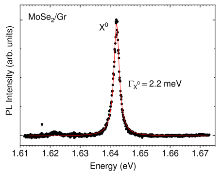
Figure S1 shows the PL spectra of another BN-capped MoSe2/graphene sample exhibiting a particularly narrow down to 2.2 meV. Although remains dominated by broadening due to disorder and dephasing, these results show that one can approach the homogeneous limit in TMD/graphene heterostructures.
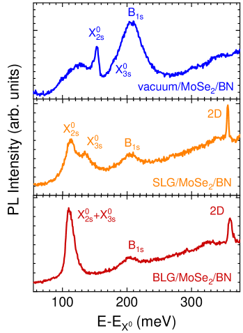
Along this line, we observed that narrow PL linewidth can also be achieved in MoSe2/graphene heterostructures without the need for an extra BN top layer. In Fig. S2, we report PL spectra of a MoSe2 monolayer deposited onto boron nitride (BN) and covered only by single (1LG) and bilayer (2LG) graphene. We observe nearly identical and narrow , near 2 meV (FWHM) in the 1LG/MoSe2/BN and 2LG/MoSe2/BN heterostructures. The PL intensity is only quenched by a factor 2.2 in 1LG/MoSe2/BN as compared to the vacuum/MoSe2/BN reference and, expectedly Chen et al. (2010) the PL quenching factor (see Table S1) only increases up to a factor of 3 in 2LG/MoSe2/BN. As we will further discuss in Sec. S9, these results demonstrate that using a single layer of graphene is an optimal solution since emission is already very efficiently filtered with minimal PL quenching (see also Table S1 and Fig. 4 in the main text for related data on SiO2 supported MoSe2/graphene).
S3 Assigning the low-energy emission lines in WSe2 and WS2
S4 Identifying the line in TMD/graphene heterostructures
S5 Supplementary discussion on the absence of PL from trions
S5a Neutralizing a TMD monolayer with graphene
Different scenarii may explain the absence of absorption and emission features in TMD/graphene. Let us first assume that the TMD coupled to graphene remains doped. Trions may then form rapidly but their slow radiative recombination (in the 20-200 ps range Robert et al. (2016); Fang et al. (2019)) is quenched by graphene. We may thus still be able to observe an absorption feature in the DR spectra, in contrast with the measurements in Fig. 2e. Furthermore, since the PL feature is more than three orders of magnitude weaker than the PL feature (see inset in Fig. 2f), the lifetime would be reduced to less than , an unrealistically low value. Alternatively, graphene may fully quench hot excitons before they can relax and form and near resident carriers. However, and formation are equally fast in MoSe2 (see Ref. Robert et al. (2016); Fang et al. (2019) and Fig. 4,5). As a result, this scenario would imply massive PL quenching, in obvious contradiction with our observations. The third and most plausible course of events is that all the native dopants in the TMD (either electrons or holes, with a typical density on the order of ) transfer to graphene, leading to a slight increase of the Fermi level of graphene (typically by less than 100 meV) and to the observation of intrinsic absorption and emission. This scenario is corroborated by room temperature Raman scattering Froehlicher et al. (2018) and PL measurements (see Fig. S7, S8).
S5b Evidence for TMD neutralization at room temperature.
S6 Exciton binding energy
Encapsulation in BN and more generally screening by a surrounding medium significantly reduce the exciton binding energy , as discussed for instance in Ref. Raja et al., 2017. In this section, we discuss PL and differential reflectance (DR) measurements, which allow us to provide a fair estimation of in our samples, also useful to estimate the changes in exciton radiative lifetime induced by graphene (see Sec. S8.1).
S6a BN capped MoSe2/graphene
First, on the BN-capped MoSe2/graphene sample discussed in Fig. 2 and 3, we find splittings between the and states and between the and states (see fit in Fig. 3c and Fig. S9).
S6b BN-supported MoSe2/graphene
We also measured and using PL spectroscopy (as in Fig. 3 and S9) in the 1LG/MoSe2/BN sample introduced in Sec. S2 (see Fig. S2). The and features nearly merge into one slightly asymmetric feature in 2LG/MoSe2/BN and we estimate . The reference region of the sample (vacuum/MoSe2/BN) displays and its 3s feature merges with the low energy wing of the hot PL feature from the 1s B exciton () that is near 210 meV above in all parts of the sample. Interestingly, although this sample is not covered by a BN thin layer, these energy shifts are very similar to the values reported in Fig. 3 and S9 in a BN-capped sample. These observations suggest that the screening experienced by a ”bare” TMD monolayer deposited onto a transparent substrate experience is marginally affected by the presence of a top dielectric layer. Let us also stress that sample to sample variations in the energy splitting between excitonic states may reflect various levels of dielectric disorder, as recently investigated in details in Ref. Raja et al., 2019.
S6c BN-capped MoS2/graphene
Similarly, using differential reflectance and PL spectroscopy, we could measure and in BN-capped MoS2/graphene and BN-capped MoS2 sample, respectively, as shown in Fig. S11.
S6d Discussion
The measured and in TMD/graphene heterostructures must be compared with the larger splittings observed TMD samples (see Fig. S9, S2, S11 and Ref. Raja et al., 2017; Han et al., 2018; Robert et al., 2018; Goryca et al., 2019), confirming appreciable reduction of in TMD/graphene heterostructures. To estimate in TMD/graphene samples, we exploit a very recent study where has been quantitatively mapped out in BN-capped TMD samples Goryca et al. (2019). For MoSe2 and MoS2, and were found, respectively, while the 1s-2s splittings were 168 meV and 170 meV, respectively.
Assuming for simplicity that the exciton binding energy reduction is proportional to the reduction of the , we can estimate binding energies in our BN-supported and BN capped MoSe2/graphene samples and 176 meV in our BN-capped MoS2/graphene sample, respectively. Our results reveal that one single layer of graphene significantly reduces by up to irrespective of the presence of a BN top layer. Our findings on are summarised in Table S2.
| Sample | |||
|---|---|---|---|
| BN/MoSe/BN (from Ref. Goryca et al., 2019) | - | ||
| BN/Gr/MoSe2/BN (Figs 2, 3 and S9) | |||
| MoSe2/BN (Fig. S10) | |||
| Gr/MoSe2/BN (Fig. S10) | |||
| BN/MoS2/BN (Fig. S11) | |||
| BN/Gr/MoS2/BN (Fig. S11) | - |
S7 Estimating laser-induced heating and exciton densities
In order to estimate the laser induced heating in our measurements, we have monitored the energy and linewidth ( and ) as a function of the incoming photon flux . As shown in Fig. S12 (data extracted from the spectra in Fig. 3a), we only observe minimal downshifts of at most 2 meV, associated with spectral broadening up to 1.5 meV. Considering the temperature dependence of and , we can conservatively estimate that the temperature laser induced temperature rise at our sample is well below 30 K up to incoming photon flux and remains below 70 K at up to the highest values of employed in our study.
Regarding the steady state excitonic density, we assume that we are in the linear recombination regime since the PL intensity is linearly increasing with . Assuming an lifetime of 2 ps (see Fig. 4 and Fig. 5) and an absorption coefficient near at 2.33 eV Li et al. (2014), we can estimate maximal injected densities of hot excitons ) for the range of employed in Fig. 3. Note also that time-resolved PL measurements were performed using picosecond oscillators with pulse fluence below a few . In these experiments, the laser photon energy was tuned between the 1s () and 2s () excitonic states. Assuming a conservative upper bound of for the MoSe2 monolayer absorptance in these conditions, we can estimate that does not exceed , values for which we have verified that our samples were still in the linear regime.
S8 Supplementary discussion on exciton dynamics
In this section, we provide additional insights into the physical origin of the PL quenching discussed in the main text and give an estimate of the non-radiative exciton transfer time to graphene and of the PL quantum yield.
As already introduced, the relaxation of in TMD is essentially radiative with a short lifetime of typically a few ps Robert et al. (2016); Palummo et al. (2015); Fang et al. (2019). In PL measurements, TMD samples cannot be resonantly excited at the energy and the state is populated after phonon-assisted relaxation of hot excitons (denoted ), on a timescale (see inset in Fig. 4a). Now, and hence the formation and relaxation dynamics depend strongly on the environment. Due to a larger disorder, or less in SiO2 supported samples Robert et al. (2016), whereas relaxation can be as long as in state of the art BN-capped samples Fang et al. (2019). This value is significantly longer than , irrespective of modifications of due to dielectric screening and to the Purcell effect Fang et al. (2019). In addition, exciton dynamics and in particular relaxation a priori depend on the incoming photon energy.
S8a Radiative liftetime and exciton transfer time
For the sake of simplicity, in Fig. 4 of the main text, we have presented a low-temperature time-resolved PL (TRPL) study of a SiO2 supported MoSe2 monolayer partially covered by a graphene monolayer. In such a samples, the formation of is faster than their radiative decay and cannot be experimentally resolved. Therefore, the TRPL measurements in Fig. 4 can safely be fit to the convolution of our IRF and an exponential decay. We have found nearly equal excited state lifetimes in graphene/MoSe2/SiO2 and in vacuum/MoSe2/SiO2 (see Fig. 4b,c), suggesting that the non-radiative transfer time of excitons to graphene is significantly longer than in graphene/MoSe2/SiO2. Let us note, however, that due to dielectric screening, is expected to be slightly longer in graphene/MoSe2/SiO2 than in vacuum/MoSe2/SiO2. As a result, observing similar in graphene/MoSe2/SiO2 and in vacuum/MoSe2/SiO2 may be coincidental and result from a compensation between the increase of and a contribution from non-radiative energy transfer of with a timescale .
As discussed in Sec. S6, screening of the Coulomb interactions induced by semi-metallic graphene reduces the exciton binding energy or equivalently increases the exciton Bohr radius. Thus, the radiative lifetime, which scales as , will increase due to the presence of graphene Robert et al. (2016). Taking the values shown in Table S2, we can estimate that in BN-capped MoSe2/graphene is approximately 2 times longer than in the bare MoSe2 reference. A similar value is obtained for the BN/MoSe2/graphene sample discussed in Fig.S2 and Fig. S10 that is not covered by a top BN layer and hence has a layout similar to the SiO2 supported sample discussed in Fig. 4. Considering the radiative lifetimes in MoSe2 monolayers (see Fig. 4 and Fig. 5), we estimate that and the exciton transfer time to graphene are both close to 5 ps at cryogenic temperatures (here 15 K). Note that as described in the main text and in Sec. S8.3, the transfer of to graphene is likely to be more efficient than the transfer of zero momentum, optically active .
Let us point out that the presence of a single layer of graphene with larger refractive index than BN may further increase . However, as discussed in Ref. Froehlicher et al. (2018); Fang et al. (2019), the inclusion of an atomically thin layer in a multi-layered system has a negligible effect on the local field enhancement experienced by the TMD monolayer and we can safely consider that changes in in TMD/graphene heterostructures essentially stem from screening of the Coulomb interactions induced by graphene.
S8b Emission quantum yield of the state
We first define the total emission quantum yield as the number of emitted photons divided by the number of absorbed photons. The latter is defined as: , with , the number of emitted photons divided by the number of cold (i.e, excitons with center of mass momentum within the light cone) and the formation yield of cold (number of cold / number of absorbed photons). In practice, due to the limited collection efficiency in cryogenic optical setups and uncertainty in the sample absorptance, it is extremely challenging to measure accurately at low temperatures. We can, however, estimate .
Indeed, it was established in Ref. Robert et al., 2016; Fang et al., 2019 that at cryogenic temperatures (typically below 90 K), recombination in MoSe2 monolayers is essentially radiative such that the measured lifetime can be attributed to the radiative lifetime . In other words is very near at low temperatures in MoSe2 monolayers. Now, using the results in Fig. 4 and Fig. 5 and the discussion in Sec. S8.1, one obtains both in SiO2 supported and BN-capped MoSe2/graphene heterostructures. Besides, the yield also depends strongly on whether the TMD under study is a bright or dark material. In the case of bright (e.g., MoSe2) TMDs, is limited by exciton transfer to graphene (in the case of graphene/TMD heterostructures) and by the presence of residual dopants (in the case of bare TMD), traps and neutral defects (in both TMD and TMD/graphene). In the case of dark (here W-based) TMDs, the population is also limited by the presence of lower lying dark states () that can be efficiently populated from the state. In WS2/graphene and WSe2/graphene heterostructures, formation of is also limited by transfer to graphene. As a result, and will be intrinsically smaller in W-based TMDs than in MoSe2, whether or not these TMDs are coupled to graphene.
S8c Photoluminescence excitation spectroscopy
In Fig. 4 and Fig. 5, care has been taken to investigate exciton dynamics using excitation only 100-110 meV above the line in MoSe2, i.e., below or close to the line. This configuration is the same as in Ref. Robert et al., 2016 and Fang et al., 2019. Noteworthy, it was reported in Ref. Fang et al., 2019 that exciton dynamics in BN-capped MoSe2 and in particular the hot exciton relaxation time (i.e., the formation time) is independent on the energy difference between the line and the incoming photon energy for .
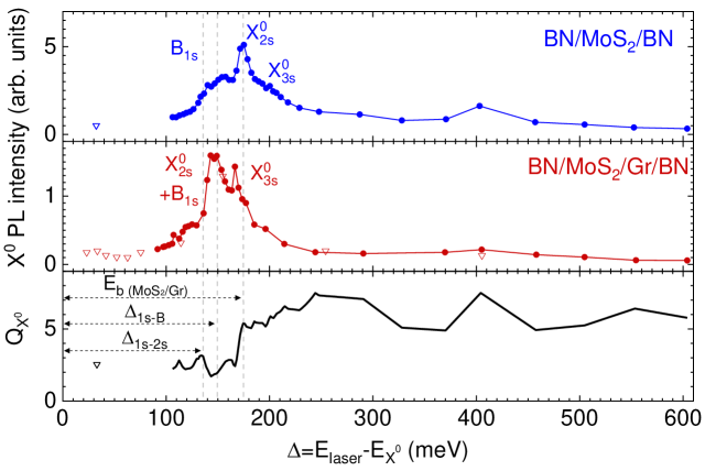
To get more insights into dynamics and PL quenching, we have performed photoluminescence excitation spectroscopy (PLE) and extracted the PL quenching factor (see Table S1) as a function of . We have chosen to focus our study on BN-capped MoS2/graphene sample shown in Fig. S11. In contrast to bare MoSe2, which shows sizeable emission from (see Fig. 4 and Fig. 5), our bare MoS2 references display minimal emission (see Fig. 1 and Fig. S11), which allows us to compare dynamics in MoS2 and MoS2/graphene without considering a significant contribution from . Our main results are shown in Fig. S13. PLE spectroscopy permits to identify the and excitons, that have unambiguously been assigned by means of DR and PL measurements (see Fig. S11). The quenching factor reaches low values for , i.e., significantly below and remains roughly constant down to . Except for strictly resonant excitation of excited excitonic states (e.g., ), no optically active excitons can be formed through vertical transitions. Instead, hot 1s excitons with finite center of mass momentum are formed through acoustic and optical phonon assisted processes and relax to form cold within the light cone. We attribute the residual PL quenching to non-radiative transfer of hot and cold excitons to graphene. Remarkably, rises sharply up to approximately 5 to 7 above , a value that precisely coincides with the state in bare MoS2 but also with the exciton binding energy in MoS2/Graphene (as shown in Table S2). Above this threshold, does not significantly increase further as augments up to . These results suggest that the rise of near cannot solely be assigned to a resonance with the state in MoS2 but suggests that generated above the free carrier continuum associated with the A excitonic manifold (for instance, hot B excitons) have a higher transfer efficiency to graphene than hot excitons.
S9 PL of a TMD monolayer onto a metal thin film.
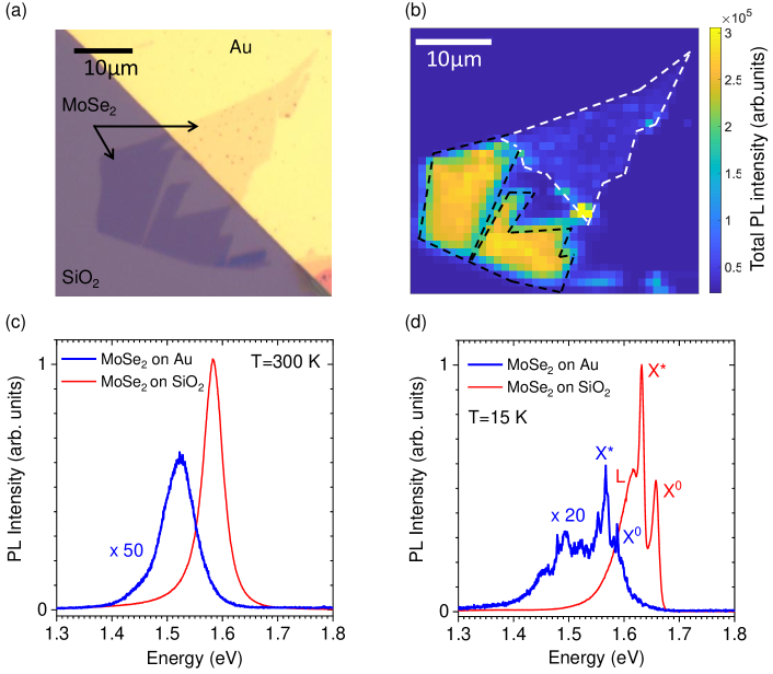
Using a 2D metallic layer such as graphene instead of a thin film of bulk metal is certainly advantageous in view of applications. Our work establishes that a single atomic layer of graphene warrants highly efficient filtering based on selective energy transfer. Nevertheless, thin films of bulk metals, such as Au, Ti, Pt…are routinely used as electrical contacts to 2D materials in electronic and optoelectronic devices and deserve special attention. Metallic thin films will be unavoidably rougher than 2D materials all the more so if the 2D materials are deposited on Boron Nitride (BN). As a result, van der Waals coupling between a metal film and an atomically thin semiconductor will be weaker than within a van der Waals heterostructure and the metal/TMD interface will be much more inhomogeneous than a van der Waals heterointerface. Such inhomogeneities are prone to affect the emission characteristics of the TMD monolayer.
As shown in Fig. S14, we have performed PL experiments on a MoSe2 Monolayer deposited onto a 60 nm-thick Au film and compared the PL spectrum of MoSe2 on Au to that of a neighbouring region of the MoSe2 flake lying onto SiO2. At room temperature, we observe large PL quenching (akin to previous findings Froehlicher et al. (2018); He et al. (2014)) and significant broadening of the PL spectra suggesting nanoscale variations of the coupling between MoSe2 and Au. At low temperature, we observe a complex, even broader PL spectrum, where the and lines can tentatively be identified. In stark contrast with the case of TMD/graphene heterostructures, we still observe strong PL quenching, sizeable emission, as well as evidence for disorder, inhomogeneous broadening and exciton localization, as shown in Fig. S14d. In other words, while the PL spectrum of MoSe2/graphene only reveals intrinsic emission, even when the MoSe2 layer lies on SiO2 (see Fig. 4 and Table S1), MoSe2 on Au displays prominent extrinsic PL features. It is therefore clear that using layered metals, ideally in the 2D limit is undoubtedly preferable than using bulk metals in view of the photonic and optoelectronic applications based on the concepts introduced in our manuscript.