Analytical modeling of orientation
effects in random nanowire networks
Abstract
Films made from random nanowire arrays are an attractive choice for electronics requiring flexible transparent conductive films. However, thus far there has been no unified theory for predicting their electrical conductivity. In particular, the effects of orientation distribution on network conductivity remain poorly understood. We present a simplified analytical model for random nanowire network electrical conductivity that is the first to accurately capture the effects of arbitrary nanowire orientation distributions on conductivity. Our model is an upper bound and converges to the true conductivity as nanowire density grows. The model replaces Monte Carlo sampling with an asymptotically faster computation and in practice can be computed much more quickly than standard computational models. The success of our approximation provides novel theoretical insight into how nanowire orientation affects electrical conductivity, illuminating directions for future research.
I Introduction
Transparent conductive films are a crucial component of touch screens and solar cells, among various other electronics [1, 2]. One approach to making transparent conductive films that has been widely studied and deployed is to randomly disperse highly conductive nanowires into a substrate. Films made in this way, using conductive material such as silver nanowires or carbon nanotubes, display competitive electrical and optical properties to alternatives, while being cheaper and more flexible than the performance standard Indium Tin Oxide [3, 4, 5, 6, 7]. The latter property is particularly valuable as flexible electronics continue to become more mainstream in consumer devices. However, despite the wide interest in applying them, there is no unified theory for predicting electrical properties of random nanowire networks, and many observed effects have not been fully characterized or explained. As a result, the technology remains underdeveloped, and there is undoubtedly still room for improvements in performance.
The majority of results describing properties of random nanowire networks have been experimental or via direct computational simulation. Various studies have experimentally compared electrical properties of films using different conductive rods, such as silver nanowires and carbon nanotubes [4, 5, 8]. Agreement between simulation and experimental observations of electrical properties has also been well established for the classes of random nanowire networks that are easiest to produce experimentally [9]. More recently, computational models have been used to maximize electrical performance of random nanowire networks by varying the distributions from which the networks are sampled [10, 11, 12, 13, 14, 15, 16, 17]. Some of these results have been verified experimentally [18, 19, 20, 21]. In particular, various computational studies have demonstrated that it is possible to improve electrical conductivity of nanowire networks by controlling nanowire orientation [10, 11, 12, 13, 14, 15, 16]. However, this effect is not well understood and there is no simple framework to predict the result of using a specific, arbitrary orientation distribution.
Recently, a number of analytical models have also been developed to describe properties of random nanowire networks, but none thus far have explained the effect of nanowire orientation on electrical conductivity in full generality [22, 23, 24, 25, 26, 27, 28, 29]. Forro et al. proposed a model derived assuming high nanowire density, so that potential drop across nanowire networks can be assumed to be linear [25]. The model is accurate in the high density regime and yields a closed-form expression. Benda et al. obtained a closed form expression for network conductivity by numerically fitting a physically interpretable form to Monte Carlo simulations, while Manning et al. developed a theoretical framework for analyzing both electrical and optical performance of nanowire networks [28, 26]. However, these models are developed under the assumption of uniformly distributed wire orientation and do not generalize in a clear manner to random orientation of an arbitrary distribution.
In this work, we present the first analytical model for random nanowire network conductivity that accurately captures the effects of arbitrary distributions of nanowire orientation. Our approximate model replaces Monte Carlo sampling with an asymptotically less expensive computation and is empirically much faster than standard computational models. It approaches the limiting dependency of network conductivity on nanowire density, with small errors even at moderate nanowire densities. Furthermore, the structure of our approximations provides novel intuition for how orientation affects network conductivity as well as intuition for the behavior of random nanowire networks in general.
II Model Construction
II.1 Setting
We begin by presenting the setting in which we develop our model. We consider networks comprised of 1-dimensional nanowires (linear, widthless sticks) inside a square space of unit length in each direction with periodic boundary conditions at the top and bottom. To simplify notation, we assume nanowires have fixed length , but our approach generalizes naturally to having a random distribution over wire length. Each nanowire is described by an coordinate pair and an angle , where the coordinate pair represents the location of the wire center and is the angle relative to the horizontal. The coordinates and the angle are sampled randomly, where all values are assumed independent and each nanowire in a network is assumed to be independent. We denote the sampling distributions of by , respectively.
The primary electrical property of interest for random nanowire networks is the sheet conductivity , which is a random variable. Sheet conductivity transitions sharply from being zero with overwhelming probability to being greater than zero with overwhelming probability at a particular number of nanowires that is a function of , known as the percolation threshold [30]. The dimensionless quantity
| (1) |
where is the number of nanowires in an network and indicates the wire length normalized by dividing by box width, is often used as a normalized concentration of nanowires because it allows direct comparison to the percolation threshold [10]. We assume that our nanowire networks are well above the percolation threshold so that they are guaranteed to have conductivity greater than zero. We focus on modeling the expected value of the sheet conductivity , because the variance of sheet conductivity is typically small relative to the expected sheet conductivity for large [9, 10].
Figure 1 displays how the sheet conductivity is physically defined, using a network sampled with nanowire positions and orientations both distributed uniformly. We place electrodes at the left and right boundary of the network ( and ) and calculate the current when 1 volt is applied. This current can then be used to calculate the sheet conductivity. In general, there are three sources of resistance in nanowire networks which determine the conductivity along with the geometry. These three sources are the resistance of wires themselves, the resistance at the junctions between two wires, and the resistance at the junctions between a wire and an electrode. In many real nanowire networks, the wire resistance is small compared to the resistance at junctions [9]. We assume that this is the case and choose to ignore the wire resistance moving forward. However, our method can be generalized to account for wire resistance, and we discuss this in Section V. We set the resistance between two wires to be a constant and set the resistance between a wire and an electrode to be a constant . The conductivity of a particular network is determined solely by the ratio between these two quantities up to scaling. We expect the wire-wire resistance to be multiple orders of magnitude larger than the wire-electrode resistance, and these quantities are thus reasonable.

In this setting, can be calculated exactly for a particular network from the symmetric adjacency matrix of the electrical network, which we denote as . The first rows of this matrix each correspond to a single wire, while the last two rows correspond to the left and right border electrode. An off-diagonal element of the matrix is 1 if the two corresponding objects touch, and all diagonal elements are 0. From , we can use the two resistance values to construct the Laplacian matrix of the nanowire network , of the same shape as . This is the matrix that, when multiplied by the vector of node voltages , gives the vector of node net current flow as given in Eq. (2), and is a linear function of [31].
| (2) |
We can then calculate the current flowing from the left electrode by setting the voltages at the left and right electrodes in the vector and solving for the remaining voltages. Dividing this current by the applied voltage yields the sheet conductivity [31].
II.2 Model definition
The expected sheet conductivity has most often been studied by direct sampling of nanowire networks [9, 10, 11, 12, 13, 14, 15, 17, 16]. This procedure involves numerous steps. For each network, nanowires are sampled according to the distributions . Then, the adjacency matrices for the networks are generated. From these matrices, observations of the sheet conductivity can be calculated by applying Kirchhoff’s Laws, which are then averaged to yield an estimate. We denote this empirical estimate by , defined in Eq. (3), where refers to the sheet conductivity of the network represented by the adjacency matrix .
| (3) |
While this approach converges rapidly to as the number of sampled networks increases, it has a number of drawbacks. First, it is slow: calculating the adjacency matrix from a list of wire coordinates and angles requires checking all pairs of nanowires for intersection, as well as computing a Cholesky decomposition of an matrix. While there are methods to speed up both of these steps, the procedure is still at least and so collecting many samples for high conductivity films is slow. In addition, this sampling based procedure makes interpretation of observed effects difficult, which limits physical intuition.
An exact analytical model for the sheet conductivity would fix these issues, but directly deriving an expression for is very difficult even under the simplest distributions . A common approximation for this type of problem is to move the expectation inside of the complicated function, as shown in Eq. (4). The right side of this equation is defined by treating as a weighted adjacency matrix; the Laplacian is constructed from by the same linear relationship as for an ordinary adjacency matrix , and the sheet conductivity is calculated by solving the same matrix equation involving .
| (4) |
However, this naive approach fails catastrophically for random nanowire networks. None of the spatial structure of the networks is captured because all nanowires are indistinguishable according to . Using as a model results in a massive overestimate of the sheet conductivity that is not useful.
To develop our analytical model, we modify the approach of moving the expectation inside the function to directly capture spatial structure of random nanowire networks. We first observe that is clearly invariant to reindexing the wires in a network and recalculating the adjacency matrix accordingly. We choose to assume, without loss of generality, that the wires are always reindexed according to increasing -coordinate. Specifically, define the random matrix as
| (5) |
where the function gets the placement of in the list of -coordinates when sorted from smallest to largest and leaves the electrode indices fixed. Our approximate model is then defined in Eq. (6), where is defined in the same way as the right side of Eq. (4).
| (6) |
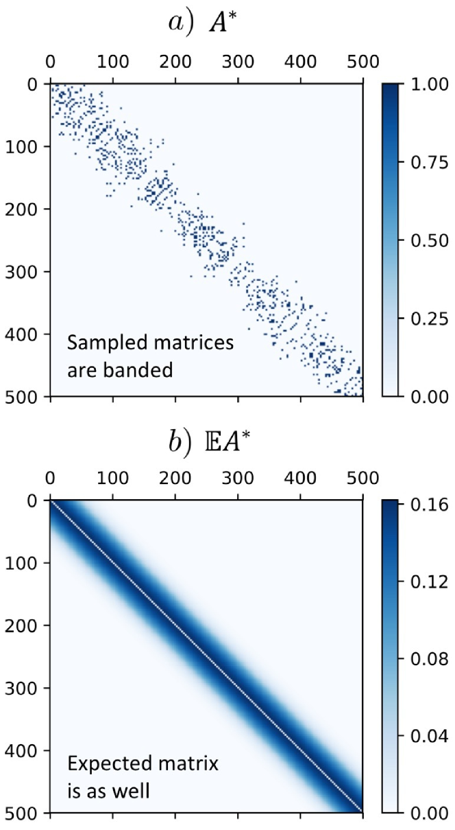
Under slightly more restrictive assumptions, we can prove that is greater than for all using Jensen’s inequality; details are presented in Section II.C. Despite being an upper bound, is able to capture the dependency of conductivity on both wire concentration and orientation distribution due to the choice of assumed wire permutation; encodes most of the spatial structure of the networks. We illustrate this property of our model in Figure 2 by plotting the values of a random sorted adjacency matrix as well as the values of under the same distributions. Due to the sorted order that is assumed, the matrices for sampled random networks are banded, because wires near in index are also near in -coordinate and therefore more likely to intersect. The expected adjacency matrix reproduces this key property well.
In the true system, nanowires that intersect are close in -coordinate as well as in -coordinate. We encode this effect only with respect to -coordinate and not -coordinate, but our empirical results verify that our model is useful regardless. This result has interesting implications which we discuss in Section IV.
II.3 Proof that is an upper bound
We argue that is an upper bound on under slightly more restrictive assumptions. Note that the Laplacian matrix for a particular nanowire network is a linear function of the sorted adjacency matrix [31]. It satisfies the Kirchhoff current equation given in Eq. (2), where is the vector of voltages at each of the objects and , the net current flowing into each node, is zero at all nodes other than the electrode nodes. To reduce notation for units, we assume in this section that is made dimensionless by dividing each element by . and then both have units of inverse resistance.
Under the assumed normalization of , the sheet conductivity is equal to the current flowing out of the left border electrode (node ) when we set the voltage at the left border to be 1V and the voltage at the right border to be 0V (, ). With these values of set, the Kirchhoff current equation is given by Eq. (7).
| (7) |
We use the notation to refer to the submatrix of from rows to and columns to . A single index indicates taking a single row or column.
We proceed by adding two minor assumptions. We first assume that for fixed distributions , the number of nanowires crossing the left electrode is a constant integer . For the high density networks we study, the variance of this quantity is small with respect to its expected value and does not cause much variance in sheet conductivity. Second, we assume that the nanowires that cross the left border are the first indices in . Under the sorting that is used for , this is the most likely set of wires to cross the left border, and the variance of these indices also does not cause much variance in sheet conductivity. This assumption can be viewed as a definition of sheet conductivity where we attach our left electrode to the leftmost wires based on center location, as opposed to based on left endpoint location.
Under these assumptions, the sheet conductivity is given by Eq. (8), where is the wire-electrode resistance in Ohms and is the dimensional vector that is 1 in the first elements and 0 otherwise.
| (8) | |||||
The inverse of exists when the network is connected, which is true because we assume that our networks are well above the percolation threshold.
Since the first nanowires cross our left measurement electrode, is given by
| (9) |
We can use this value to write another expression for in Eq. (10).
| (10) |
Since is assumed to be constant, the only randomness in comes from . Since this matrix is positive definite when the network is connected and is a linear function of , is a concave function of . Jensen’s inequality then tells us that for all , is an upper bound on as shown in Eq. (11).
| (11) |
III Model computation
III.1 Methods for computing
The approximate model is useful because we can directly compute in a wide variety of circumstances. This eliminates the need for Monte Carlo sampling of networks and solving a linear system of equations for each sample. Here we present a method for computing when are the uniform distribution, which is an assumption used throughout the literature. This procedure is applicable for any orientation distribution that can be parameterized by a vector .
Recall that is the sorted adjacency matrix of a random nanowire network and has size . The first indices correspond to a nanowire, sorted by increasing -coordinate, while indices and correspond to the left and right border electrode. The elements of the expected adjacency matrix are thus the probability of intersection between the objects of indices . To compute the matrix, we thus need to compute the probability of intersection between every pair of wires, conditioned on the rank of the -coordinate of each wire. We also need to calculate the probability of intersection between each wire and the border electrodes, conditioned on the rank of the -coordinate of the wire. Because the matrix is symmetric, we only need to do so for , and we only need to do the calculation for a single border electrode because the probabilities for the other border electrode are symmetric.
We will first calculate the probability of intersection between any two nanowires. Denote a wire as and let be the th and th wire according to the sorted order based on -coordinate. The desired probability is then denoted by . The event of intersecting is a deterministic function of the difference in coordinates, the difference in coordinates, and the angles of the two wires. Under our independence assumptions, we can thus calculate by calculating the distributions of and and then using the known distributions of and . For brevity, we define
| (12) | |||||
| (13) |
We will first analyze randomness solely in by computing the intersection probability conditioned on , denoted by . This is the probability that two wires intersect if we know the difference in -coordinates between them. For any pair of wires with -separation and angles , we can define the horizontal range of overlap as the length of the interval of -coordinates that both wires lie in. For particular values of , there is an interval of values for which and will cross. We denote the length of this interval of by . We illustrate these quantities with example nanowire pair configurations in Figure 3.

Now observe that the distribution of is identical for all . Furthermore, because of our use of periodic boundary conditions, since is the uniform distribution, is in fact the uniform distribution in the range . Therefore, the probability of intersection between and conditioned on is given by the conditional expectation of :
| (14) |
We can calculate this conditional expectation by observing that and can be calculated from and , as in Eq. (15, 16). Here, is defined to be .
| (15) | ||||
| (16) |
In Eq.(15), the latter two cases correspond to the situation when the interval of -coordinates that one wire lies in is contained by the interval of -coordinates that the other lies in, as in Figure 3a. The first case is taken when this situation does not occur, as in Figure 3b.
The conditional expectation is then given by integrating out and drawn independently from :
| (17) |
Since we have assumed the wires are sorted by -coordinate, the difference is the difference in order statistics and from the distribution . Because is the uniform distribution, follows the Beta distribution with parameters and , if [32]. However, for the networks with large which we study, these distributions become strongly concentrated at their mean, which is . We thus assume that is equal to its expected value, and empirically observe no loss in accuracy. This yields a formula for the probability of intersection between any two nanowires:
| (18) |
A similar argument can be used to calculate the probability that any wire crosses the left border electrode, denoted by . Observe that intersects if and only if . Assuming that equals its expected value of , the desired probability is then given by Eq. (19), where .
| (19) |
We can therefore calculate every element of for any and any orientation distribution , assuming wire positions are uniform.
To use these expressions efficiently, we numerically compute the integral in Eq. (17) over a grid of values for and the parameters of the orientation distribution . We then fit a polynomial to the probability values on these grid points to obtain an expression for that is extremely rapid to use. We further describe the speed of our method in the next subsection.
III.2 Analysis of computational speed
One of the significant advantages of our method is that it replaces Monte Carlo sampling with an asymptotically faster computation. Sampling-based models, which are the most common approaches for studying random nanowire networks, have two major components. First, a number of nanowire networks are sampled by directly sampling for each of nanowires, and a collection of adjacency matrices are calculated. Second, the Kirchhoff current equation is solved for each adjacency matrix to collect observations of sheet conductivity, and these observations are then averaged. The first of these steps has complexity . Within all networks, each of the nanowires must be compared with a fixed fraction of all other nanowires for intersection to compute the adjacency matrix . The second step, meanwhile, has complexity , which is the cost of solving linear systems of equations each involving variables. While the second step has larger complexity, both steps require significant amounts of time and so speeding up either is beneficial.
Our model delivers a large asymptotic improvement to the first step and delivers a large constant factor improvement to the second step. Recall that the probability of intersection between two wires under our model depends only on the expected -separation between them. As a result, we only need to directly compute two rows of in order to produce the entire matrix. This is because the expected -separation between the wires and is determined completely by the quantity . Equivalently, if we ignore the rows representing electrodes, then all diagonals of are constant. We therefore must compute the first row of to obtain the probability of interaction between every pair of nanowires, and also must compute the last row of to obtain the probability of interaction between every nanowire and an electrode. Therefore, the cost of computing is with constant proportional to the time it takes to compute . We must still solve a single Kirchhoff current equation, and this step is .
Numerically integrating to compute each evaluation of is in practice quite slow. We therefore precompute this function for a grid of values of as well the parameters of the orientation distribution , and then fit a polynomial to the computed values. A polynomial fit is in practice quite accurate because the probability in question is smooth as a function of the parameters of interest. This step makes computation of extremely rapid, but the precomputation cost is exponential in the number of parameters of the orientation distribution. For the majority of interesting cases, the orientation distribution can be parameterized in one or two parameters, and this complexity is thus not significant compared to other steps.
In total, our method has a small precomputation cost, but replaces the complexity of Monte Carlo sampling with an asymptotically faster computation. It also reduces the cost of solving linear systems by a factor of , the number of samples that are collected in a sampling based approach. In our implementation, this allowed the model to be evaluated about 100 times faster than direct Monte Carlo sampling.

IV Empirical Tests and Discussion
We examine the effectiveness of in modeling dependency of network conductivity on both nanowire density and orientation distribution. We assume, as in the previous section, that are both the uniform distribution. We implemented direct sampling of under this assumption and our previously stated setting, while allowing the distribution to be arbitrary. We use our implementation of direct sampling of as a baseline comparison for all tests, estimating with with . Throughout these experiments, we use . Larger values of reduce the noise of , while smaller values of reduce finite size error in and . The chosen values of and were found empirically to be sufficient to largely eliminate these errors; and do not change much for higher or lower , as long as is fixed.
IV.1 Dependence on nanowire density
We first assume that is the isotropic distribution (uniform in degrees) and explore the dependence of on normalized concentration . Figure 4 shows a comparison between normalized and as a function of , starting just above the percolation threshold, on both linear and double log scales. Conductivities are normalized by multiplying by junction resistance so that they are unitless. It is a known result that can be approximated as a power law function of the distance of normalized concentration from the percolation threshold, with an exponent of around 1.75 at medium densities which moves close to 2 at high densities [9]. Our estimate matches these known relationships; the growth pattern of conductivity in log-space becomes linear as the subtraction of the percolation threshold becomes negligible. Our model , however, displays a perfect power law dependence on , with an exponent that matches the asymptotic exponent of . Near the percolation threshold, the error is large, as we have assumed nanowire density above this threshold in developing our model. However, the error in log space approaches zero as concentration grows, and the model can thus be interpreted as the limiting behavior of at high concentrations.
While is less precise than other recent models for predicting dependency of conductivity on concentration at small nanowire densities, the result that our approach yields the correct limiting behavior is theoretically interesting. By using , our model directly encodes clustering of nanowire only in the -direction. However, this is sufficient information to capture asymptotic behavior, and, as we next show, capture the effect of varying orientation distribution.

IV.2 Dependence on orientation distribution
Our model is particularly valuable because it is able to predict the effect of arbitrary orientation distributions on sheet conductivity. The problem of optimizing orientation distribution in random nanowire networks has been studied numerous times via computational models, but there is no unified understanding of the observed effects [11, 13, 14, 16, 10].
We consider two families of distributions for , each of which is described by a single parameter. For each family, we demonstrate that accurately captures the effect of varying the distribution parameter on conductivity. The first family is given by
| (20) |
for all . All probability mass is concentrated at degrees from horizontal. The second family is given by
| (21) |
Probability density is uniformly distributed over degrees. Figure 5 shows a sample network from a single distribution within each family. These two families were previously studied, and it was found that while a conductivity gain over isotropic networks could be achieved within , no gain could be achieved within [10].

Figure 6 shows a comparison between and for determining the relationship between distribution parameter and normalized conductivity for both and . The normalized concentration is fixed at 50 in both cases. Within both families, the shape of the curve matches well, and the optimal values are within a few degrees of each other. Moreover, the predictions from match in that a gain over isotropic orientation is attainable in but not .
To the best of our knowledge, our model is the first to accurately reproduce the effects of orientation distribution on sheet conductivity without relying on Monte Carlo sampling in any capacity. These results indicate that orientation effects can be modeled by analyzing their effects on network connectivity in a single direction, as our model only takes into account positions of nanowires in the -direction.
V Conclusion
We developed an approximate analytical model for sheet conductivity of random nanowire networks that condenses a large amount of their structure through a specific choice of nanowire permutation. We showed that this model is an upper bound and matches the asymptotic dependency of the true sheet conductivity on wire concentration. We also demonstrated that the model accurately captures the effects of orientation on nanowire network conductivity, a result that has limited theoretical explanation in the literature. Our model is the first to accurately capture the effects of arbitrary orientation distributions on network conductivity, and replaces Monte Carlo sampling with an asymptotically faster computation. These results and the structure of the model we developed provide novel theoretical intuition about random nanowire network conductivity. Namely, our results demonstrate that network connectivity in the direction of current flow is the key factor in determining the dependence of conductivity on wire density and orientation distribution, because our model only encodes connectivity information in the -direction.
The most pressing direction for future research is to relax our assumption of zero wire resistance, as recent work has indicated that the junction resistance in silver nanowire networks can be reduced to a comparable magnitude as the wire resistance [18]. This could be done, for example, by using an approximate function to calculate sheet conductivity based on in the presence of wire resistance. Various recent analytical models for random nanowire network conductivity have successfully used approximations about the number of nanowires that a given nanowire will intersect [29, 25]. Rather than using approximations derived in the setting of uniform wire orientation, these models could instead use approximations obtained from for an arbitrary orientation distribution. The success of these existing models indicates that they would likely function as accurate approximate functions to calculate sheet conductivity given the information in .
References
- Kumar and Zhou [2010] A. Kumar and C. Zhou, ACS nano 4, 11 (2010).
- Gordon [2000] R. G. Gordon, MRS bulletin 25, 52 (2000).
- Choi et al. [2019] S. Choi, S. I. Han, D. Kim, T. Hyeon, and D.-H. Kim, Chemical Society Reviews 48, 1566 (2019).
- Hecht et al. [2011] D. S. Hecht, L. Hu, and G. Irvin, Advanced materials 23, 1482 (2011).
- Hu et al. [2011] L. Hu, H. Wu, and Y. Cui, MRS bulletin 36, 760 (2011).
- Lee et al. [2008] J.-Y. Lee, S. T. Connor, Y. Cui, and P. Peumans, Nano letters 8, 689 (2008).
- Teymouri et al. [2017] A. Teymouri, S. Pillai, Z. Ouyang, X. Hao, F. Liu, C. Yan, and M. A. Green, ACS applied materials & interfaces 9, 34093 (2017).
- Marus et al. [2015] M. Marus, A. Hubarevich, H. Wang, A. Stsiapanau, A. Smirnov, X. W. Sun, and W. Fan, Optics express 23, 26794 (2015).
- Mutiso et al. [2013] R. M. Mutiso, M. C. Sherrott, A. R. Rathmell, B. J. Wiley, and K. I. Winey, ACS nano 7, 7654 (2013).
- Jagota and Tansu [2015] M. Jagota and N. Tansu, Scientific reports 5, 10219 (2015).
- Behnam et al. [2007] A. Behnam, J. Guo, and A. Ural, Journal of Applied Physics 102, 044313 (2007).
- Behnam and Ural [2007] A. Behnam and A. Ural, Physical Review B 75, 125432 (2007).
- Du et al. [2005] F. Du, J. E. Fischer, and K. I. Winey, Physical Review B 72, 121404 (2005).
- White et al. [2009] S. I. White, B. A. DiDonna, M. Mu, T. C. Lubensky, and K. I. Winey, Physical Review B 79, 024301 (2009).
- Tarasevich et al. [2018] Y. Y. Tarasevich, I. V. Vodolazskaya, A. V. Eserkepov, V. A. Goltseva, P. G. Selin, and N. I. Lebovka, Journal of Applied Physics 124, 145106 (2018).
- Pimparkar et al. [2007] N. Pimparkar, C. Kocabas, S. J. Kang, J. Rogers, and M. A. Alam, IEEE electron device letters 28, 593 (2007).
- Hicks et al. [2018] J. Hicks, J. Li, C. Ying, and A. Ural, Journal of Applied Physics 123, 204309 (2018).
- Bellew et al. [2015] A. T. Bellew, H. G. Manning, C. Gomes da Rocha, M. S. Ferreira, and J. J. Boland, ACS nano 9, 11422 (2015).
- Ackermann et al. [2016] T. Ackermann, R. Neuhaus, and S. Roth, Scientific reports 6, 34289 (2016).
- Marus et al. [2017a] M. Marus, A. Hubarevich, R. J. W. Lim, H. Huang, A. Smirnov, H. Wang, W. Fan, and X. W. Sun, Optical Materials Express 7, 1105 (2017a).
- Wu et al. [2016] F. Wu, Z. Li, F. Ye, X. Zhao, T. Zhang, and X. Yang, Journal of Materials Chemistry C 4, 11074 (2016).
- Marus et al. [2017b] M. Marus, A. Hubarevich, H. Wang, Y. Mukha, A. Smirnov, H. Huang, W. Fan, and X. W. Sun, Thin Solid Films 626, 140 (2017b).
- Kim and Nam [2018] D. Kim and J. Nam, Journal of Applied Physics 124, 215104 (2018).
- Tarasevich et al. [2019] Y. Y. Tarasevich, I. V. Vodolazskaya, A. V. Eserkepov, and R. K. Akhunzhanov, Journal of Applied Physics 125, 134902 (2019).
- Forró et al. [2018] C. Forró, L. Demkó, S. Weydert, J. Vörös, and K. Tybrandt, ACS nano 12, 11080 (2018).
- Manning et al. [2019] H. G. Manning, C. G. da Rocha, C. O’Callaghan, M. S. Ferreira, and J. J. Boland, Scientific reports 9, 1 (2019).
- Ponzoni [2019] A. Ponzoni, Applied Physics Letters 114, 153105 (2019).
- Benda et al. [2019] R. Benda, E. Cancès, and B. Lebental, Journal of Applied Physics 126, 044306 (2019).
- Kumar et al. [2017] A. Kumar, N. Vidhyadhiraja, and G. U. Kulkarni, Journal of Applied Physics 122, 045101 (2017).
- Stauffer and Aharony [2018] D. Stauffer and A. Aharony, Introduction to percolation theory (Taylor & Francis, 2018).
- Klein and Randić [1993] D. J. Klein and M. Randić, Journal of mathematical chemistry 12, 81 (1993).
- Weisberg [1971] H. Weisberg, The Annals of Mathematical Statistics 42, 704 (1971).