Mottness versus unit-cell doubling
as the driver of the insulating state in 1T-TaS2
If a material with an odd number of electrons per unit cell turns out to be insulating, Mott localisation may be invoked as an explanation Mott1937 ; Imada1998 . This is widely accepted for the layered compound 1T-TaS2, which has a low-temperature insulating phase comprising charge order clusters with 13 unpaired orbitals each Wilson1975 ; Fazekas1979 ; Fazekas1980 . But if the stacking of layers doubles up the unit cell to include an even number of orbitals, the nature of the insulating state is ambiguous Ritschel2018 ; Lee2019 . Here, scanning tunnelling microscopy (STM) reveals two distinct terminations of the charge order in 1T-TaS2, the sign of such a double-layer stacking pattern. However, spectroscopy at both terminations allows us to disentangle unit-cell doubling effects and determine that Mott localisation alone is enough to drive gap formation. We also observe the collapse of Mottness at an extrinsically restacked termination, demonstrating that the microscopic mechanism of insulator-metal transitions Stojchevska2014 ; Hollander2015 ; Vaskivskyi2015 ; Yoshida2015 ; Vaskivskyi2016 ; Cho2016 ; Ma2016 lies in degrees of freedom of interlayer stacking.
The undistorted high-temperature atomic structure of 1T-TaS2 is shown in Fig. 1a. Below 350 K, the Ta lattice within each layer undergoes a periodic in-plane distortion in which clusters of 13 Ta ions contract towards the central ion of the cluster forming a ‘Star-of-David’ (SD) motif Wilson1975 . Upon cooling below 180 K, this pattern locks in to become commensurate with the atomic lattice and long range order emerges, described as a triangular R13.9∘ charge density wave (CDW) pattern, depicted in Fig. 1b. Within each of the SD clusters, 12 of the Ta 5d orbitals at the periphery form 6 filled bands and leave a CDW gap Qiao2017 , stabilizing the distortion. The remaining orbital, according to band theory, should form a half-filled band, and the experimentally observed insulating behaviour is usually attributed to its localisation at the SD centre by strong electron-electron (e-e) interactions Fazekas1979 ; Fazekas1980 . From this foundation it has been suggested that, since a Mott state in 1T-TaS2 realises a triangular lattice of localised spins, it might host a quantum spin liquid (QSL), an unusual phase of quantum electronic matter in which, due to geometric frustration and quantum fluctuations, the spins refuse to magnetically order even down to = 0 K Balents2010 ; Law2017 ; Klanjsek2017 ; Ribak2017 .
The Mott state thought to exist in 1T-TaS2 is different from ordinary Mott insulators such as NiO, in that electrons localise not at the sites of the atomic crystal, but at the sites of the electronic crystal, the lattice of SD clusters, and so it is called a ‘cluster Mott insulator’. As the SD clusters must be centred on Ta sites, the three-dimensional (3D) structure formed from the layering of 2D charge order lattices can be described with stacking vectors T composed of the underlying Ta lattice vectors. Neglecting the S atomic layers sandwiching the Ta layer, there are only three symmetrically inequivalent stacking vectors: = c, = a + c, and = a + b + c (with the latter two each having a group of symmetrical equivalents). The impact of this stacking degree of freedom on the electronic structure of 1T-TaS2 was largely neglected until Ritschel et al predicted, using ab initio calculations, that different inter-layer stacking patterns could result in a metallic phase (for stacking) as an alternative to the well-known insulating phase (previously assumed to have stacking) Ritschel2015 . Going further, Ritschel et al and Lee et al recently challenged the rationale by which 1T-TaS2 was thought to be a Mott insulator, showing that if the stacking alternates between vectors and as previously suggested Tanda1984 ; Naito1984 ; Naito1986 , such that the new supercell includes two SD clusters, ab initio calculations predict an insulator without the need to invoke strong e-e interactions Ritschel2018 ; Lee2019 . More simply, if the electronic unit cell contains two SDs, the total number of electrons per cell is even, leaving the highest occupied band filled and allowing an insulator without invoking Mott. This introduces serious complication into the understanding of the insulating state in 1T-TaS2, and potentially undermines the foundations on which recent suggestions of a QSL state are built Law2017 .
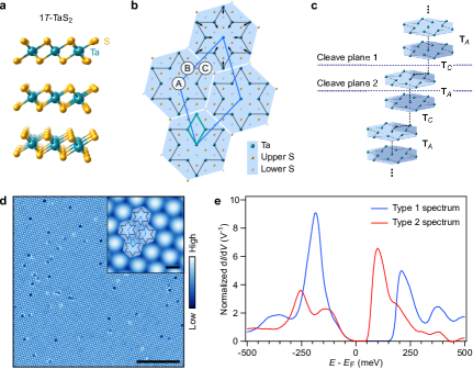
A consequence of the , , , …(henceforth ‘ACAC’) stacking pattern is that there are two cleavage planes, as indicated in Fig. 1c, yielding two inequivalent surfaces amenable to investigation using STM. One plane is located between one -stacked bilayer (BL) and another, and the other plane splits a single BL, leaving unpaired (-stacked) layers. In this work, samples were cleaved, transferred to the STM and measured at temperatures far below the transition temperature at which the commensurate CDW sets in (180 K), and the bulk structure of the CDW should be preserved such that measurements on a large number of cleaved surfaces may show evidence of the ACAC pattern. Eight platelets of 1T-TaS2 were cleaved multiple times each, for a total of twenty-four investigated surfaces, the topographic image for one of which appears in Fig. 1d. Conductance spectra were acquired at defect-free locations on each sample. Spectra showing a gap in the density of states (DOS) of 150 meV, broadly consistent with those shown in previous STM reports Cho2016 ; Ma2016 ; Cho2017 ; Qiao2017 were observed on eighteen of the twenty-four surfaces (similar to the blue curve labelled ‘Type 1’ in Fig. 1e). A different form of the DOS, with a smaller gap of 50 meV, was observed on the remaining six (‘Type 2’, the red curve in Fig. 1e). (We only consider the spectra acquired in the regions where the STM tip first arrived at the sample surface). We tentatively attribute the appearance of these two forms of DOS to the surfaces created by the two cleavage planes of the bulk stacking pattern. However, more information is needed to definitively assign each form of DOS to each cleaved surface, and we return to this below. If the number of cleavage planes of each type throughout the sample is roughly equal, as we assume, the deviation of the observed ratio from 1:1 may correspond to a difference in their associated surface formation energies, and the resulting rarity of the small-gap surface may explain its absence in previous reports. A small number of instances were observed where the two types of surface appeared side-by-side, for example on either side of a domain wall Cho2017 in the CDW pattern (see Supplementary Information).
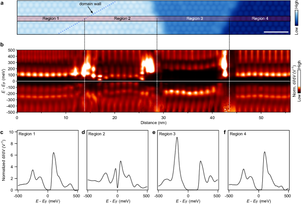
Most revealingly, the two types were also observed side-by-side where single-layer steps allowed the simultaneous observation of multiple TaS2 layers. Figure 2a shows a topographic image of three terraces, with the upper terrace featuring a domain wall (marked with a dark blue dotted line), so that four distinct regions are observed (labelled Regions 1–4). Tunnelling spectroscopy acquired along a path spanning the long axis of the topographic image (marked with a red-tinted rectangle) shows changes in the DOS spectrum upon each transition between regions (Fig. 2b). Representative spectra taken at a point within each of the four regions are shown in Fig. 2c–f. Region 2 shows a finite DOS at , reminiscent of the ‘metallic mosaic’ phase which has been created locally using STM induced voltage pulses, Cho2016 with interlayer stacking effects suggested as a possible explanation Ma2016 . Briefly postponing the discussion of this metallic phase, we first note that the form of the DOS in the other three regions is seen to alternate from one terrace to the next, from a small gap (Region 1) to a large gap in the middle terrace (Region 3), and to the small gap again at the lowest terrace (Region 4). This alternating sequence is consistent with that expected for the ACAC stacking shown in Fig. 1e. (Another, similar instance of the switching of electronic structure from one type to the other across a single layer step is shown in the Supplementary Information.)
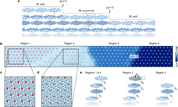
With a view to establishing which type of surface corresponds to which of the cleavage planes in the ACAC stacking pattern, we note that single-layer steps should result in an in-plane displacement, or phase jump , of the 2D projected CDW pattern from one terrace to the next, which should alternate between zero and non-zero (specifically a + b, the in-plane projection of ), as is shown in Fig. 3a. The step between Regions 3 & 4 realises the former case: In Fig. 3b, the SD centres in these two regions are highlighted with an array of white dots, showing clearly the absence of an in-plane displacement and hence indicating that in Region 3 the stacking pattern terminates with an intact BL at the surface, and that in Region 4, an unpaired layer of SD clusters remains.
The array of white dots is extended over to the left-hand-side of the image. The centres of the SD lattice in the two regions of the upper terrace are overlaid with this reference lattice to show the approximate in-plane shift. Additional atomically resolved topographic imaging in Region 1 (see Supplementary Information) is used to determine the orientation of the SD clusters, depicted in the zoom-in images of Figs. 3c,d. The in-plane components of the stacking vectors for Regions 1 & 2 are then discernible. In Region 1 the stacking vector is shown to correspond closely to , as expected for the ACAC stacking pattern, with a discrepancy well below one atomic lattice constant. The stacking vector between the metallic region, Region 2, and the underlying BL is also determined, and corresponds closely to the . As this type of metallic region was observed nowhere else throughout measurements on twenty-three other samples, we posit that it is an outcome of an extrinsic process during formation of the step-edge, such as a brief lifting of the uppermost TaS2 layer and re-stacking of its CDW into a metastable configuration.
Taken together, the observations presented in Figs. 2 and 3 form a picture which is indeed consistent with the previously suggested ACAC stacking pattern, and allow us to establish a link between the surface CDW configuration and the surface local DOS, as summarized in Fig. 3e. The spectrum observed in Region 3 with the relatively large gap of 150 meV has been reported in multiple STM works. We now suggest that this spectrum signifies a surface where the CDW terminates with the -stacked BL intact, and can be thought of as the bulk-like termination of the CDW (i.e. without major structural or electronic reconfiguration with the formation of the surface). The fact that this surface was the most common outcome from cleavage (18 out of 24) indicates the energetic favourability of cleaving between BLs, rather than through them, suggesting non-negligible intra-BL bonding.
The surface of unpaired SD clusters (Regions 1 & 4) represents a new and perhaps qualitatively distinct system. It satisfies the conditions under which 1T-TaS2 was originally thought to be a Mott insulator: A system with an odd number of electrons per (surface) unit cell, and yet which is insulating. This re-affirms the importance of strong e-e interactions in the insulating state of 1T-TaS2, complementing the recent observation of doublon excitations characteristic of a Mott state Ligges2018 . An insulating state in the unpaired layer also leaves some room for the persistence, at surfaces and possibly bulk stacking faults, of a QSL ground state despite possible inter-layer singlet formation within the bulk BLs Law2017 . It also suggests that the metallic state also observed (Region 2 in Fig. 2) is properly described as a ‘Mottness-collapsed’ state, in which the Mottness ratio has been reduced either by increased screening of the on-site Coulomb repulsion , or due to an increase of the inter-cluster overlap integral . It is noteworthy that although the DOS at is non-zero, the residual pseudogap-like features around suggest the persistence of strong e-e interactions in this metallic state.
Questions arise about the detailed mechanisms in play at these distinct surfaces – Why does the unpaired cluster layer have a smaller gap than the paired layer, and why does Mottness break down leading to metallicity for stacking? Further investigations of the detailed behaviour of the 3D electronic correlations in 1T-TaS2, especially at its surface terminations and also in few-layer or monolayer form, may prove fruitful in understanding the nature of its insulating state and its potentially useful metal-insulator transitions.
Methods
Crystals of 1T-TaS2 were synthesized using a chemical vapor transport method described previously Tani1981 , with 2 % excess S. Samples were cleaved in ultra-high vacuum (10-10 Torr) at 77 K and quickly inserted into a Unisoku 1300 low temperature STM system, of which the STM head has been replaced with a homemade one Hanaguri2006 . All measurements were performed at a temperature of 1.5 K. STM tips were formed using electro-chemical etching of tungsten wire, and after insertion into UHV, were cleaned and characterized using field ion microscopy followed by careful conditioning on a clean Cu(111) surface. STM topography images were collected in constant-current mode. For conductance curves and spectroscopic mapping on 1T-TaS2 surfaces, the lock-in technique with a bias modulation of amplitude = 10 mV and frequency = 617.3 Hz was used.
The spectroscopy data in Figs. 1 & 2, including the spatially resolved data shown in Fig. 2b, were normalized according to the current signal at = 500 mV. This somewhat compensates for the large difference in raw signal intensity caused by differing tip-sample distances while scanning at = 250 mV over areas with large or small spectral gaps.
Acknowledgements
We are grateful to Y. Kohsaka, T. Machida and P. A. Lee for helpful discussions. C.J.B. gratefully acknowledges support from RIKEN’s SPDR fellowship. This work was supported in part by JSPS KAKENHI grant numbers JP18K13511, JP19H00653 and JP19H01855.
Author contributions
T.H. and Y.I. conceived the project, and M.Y. and Y.I. synthesized the 1T-TaS2 crystals. C.J.B. performed the STM measurements with assistance from T.H., and prepared the manuscript with input from all authors.
References
- (1) Mott, N. F. & Peierls, R. Discussion of the paper by de Boer and Verway. Proc. Phys. Soc. Lond. 49, 72 (1937). https://doi.org/10.1088/0959-5309/49/4S/308
- (2) Imada, M., Fujimori, A. & Tokura, Y. Metal-insulator transitions. Rev. Mod. Phys. 70, 1039 (1998). https://doi.org/10.1103/RevModPhys.70.1039
- (3) Wilson, J. A., Di Salvo, F. J. & Mahajan, S. Charge-density waves and superlattices in the metallic layered transition metal dichalcogenides. Adv. Phys. 24, 117–201 (1975). https://doi.org/10.1080/00018737500101391
- (4) Fazekas, P. & Tosatti, E. Electrical, structural and magnetic properties of pure and doped 1T-TaS2. Phil. Mag. B 39, 229–244 (1979). https://doi.org/10.1080/13642817908245359
- (5) Fazekas, P. & Tosatti, E. Charge carrier localization in pure and doped 1T-TaS2. Physica B & C 99, 183–187 (1980). https://doi.org/10.1016/0378-4363(80)90229-6
- (6) Ritschel, T., Berger, H. & Geck, J. Stacking-driven gap formation in layered 1T-TaS2. Phys. Rev. B 98, 195134 (2018). https://doi.org/10.1103/PhysRevB.98.195134
- (7) Lee, S.-H., Goh, J. S. & Cho, D. Origin of the Insulating Phase and First-Order Metal-Insulator Transition in 1T-TaS2. Phys. Rev. Lett. 122, 106404 (2019). https://doi.org/10.1103/PhysRevLett.122.106404
- (8) Stojchevska, L. et al. Ultrafast switching to a stable hidden quantum state in an electronic crystal. Science 344, 177–180 (2014). https://doi.org/10.1126/science.1241591
- (9) Hollander, M. J. et al. Electrically Driven Reversible Insulator-Metal Transition in 1T-TaS2. Nano Lett. 15, 1861–1866 (2015). https://doi.org/10.1021/nl504662b
- (10) Vaskivskyi, I. et al. Controlling the metal-to-insulator relaxation of the metastable hidden quantum state in 1T-TaS2. Sci. Adv. 1, e1500168 (2015). https://doi.org/10.1126/sciadv.1500168
- (11) Yoshida, M., Suzuki, R., Zhang, Y., Nakano. M. & Iwasa, Y. Memristive phase switching in two-dimensional 1T-TaS2. Sci. Adv. 1, e1500606 (2015). https://doi.org/10.1126/sciadv.1500606
- (12) Vaskivskyi, I. et al. Fast electronic resistance switching involving hidden charge density wave states. Nat. Communs. 7, 11442 (2016). https://doi.org/10.1038/ncomms11442
- (13) Cho, D. et al. Nanoscale manipulation of the Mott insulating state coupled to charge order in 1T-TaS2. Nat. Communs. 7, 10453 (2016). https://doi.org/10.1038/ncomms10453
- (14) Ma, L. et al. A metallic mosaic phase and the origin of Mott-insulating state in 1T-TaS2. Nat. Communs. 7, 10956 (2016). https://doi.org/10.1038/ncomms10956
- (15) Balents, L. Spin liquids in frustrated magnets. Nature 464, 199–208 (2010). https://doi.org/10.1038/nature08917
- (16) Law, K. T. & Lee, P. A. 1T-TaS2 as a quantum spin liquid. Proc. Natl. Acad. Sci. 114 (27), 6996–7000 (2017). https://doi.org/10.1073/pnas.1706769114
- (17) Klanjšek, M. et al. A high-temperature quantum spin liquid with polaron spins. Nat. Phys. 13, 1130–1134 (2017). https://doi.org/10.1038/nphys4212
- (18) Ribak, A. et al. Gapless excitations in the ground state of 1T-TaS2. Phys. Rev. B 96, 195131 (2017). https://doi.org/10.1103/PhysRevB.96.195131
- (19) Ritschel, T. et al. Orbital textures and charge density waves in transition metal dichalcogenides. Nat. Phys. 11, 328–331 (2015). https://doi.org/10.1038/nphys3267
- (20) Tanda, S., Sambongi, T., Tani, T. & Tanaka, S. X-Ray Study of Charge Density Wave Structure of 1T-TaS2. J. Phys. Soc. Jpn. 53, 476–479 (1984). https://doi.org/10.1143/JPSJ.53.476
- (21) Naito, M., Nishihara, H. & Tanaka, S. Nuclear quadrupole resonance in the charge density wave state of 1T-TaS2. J. Phys. Soc. Jpn. 53, 1610–1613 (1984). https://doi.org/10.1143/JPSJ.53.1610
- (22) Naito, M., Nishihara, H. & Tanaka, S. Nuclear magnetic resonance and nuclear quadrupole resonance study of 181Ta in the commensurate charge density wave state of 1T-TaS2. J. Phys. Soc. Jpn. 55, 2410–2421 (1986). https://doi.org/10.1143/JPSJ.55.2410
- (23) Cho, D. et al. Correlated electronic states at domain walls of a Mott-charge-density-wave insulator 1T-TaS2. Nat. Communs. 8, 392 (2017). https://doi.org/10.1038/s41467-017-00438-2
- (24) Qiao, S. et al. Mottness Collapse in 1T-TaS2-xSex Transition-Metal Dichalcogenide: An Interplay between Localized and Itinerant Orbitals. Phys. Rev. X 7, 041054 (2017). https://doi.org/10.1103/PhysRevX.7.041054
- (25) Ligges, M. et al. Ultrafast Doublon Dynamics in photoexcited 1T-TaS2. Phys. Rev. Lett. 120, 166401 (2018). https://doi.org/10.1103/PhysRevLett.120.166401
- (26) Tani, T., Okajima, K., Itoh, T. & Tanaka S. Electronic transport properties in 1T-TaS2. Physica B & C 105, 127–131 (1981). https://doi.org/10.1016/0378-4363(81)90230-8
- (27) Hanaguri, T. Development of high-field STM and its application to the study on magnetically tuned criticality in Sr3Ru2O7. J. Phys. Conf. Ser. 51, 514 (2006). https://doi.org/10.1088/1742-6596/51/1/117