Simple Thermal Noise Estimation of Switched Capacitor Circuits Based on OTAs – Part II: SC Filters
Abstract
In Part I of this paper, we have shown how to calculate the thermal noise voltage variances in switched-capacitor (SC) circuits using operational transconductance amplifiers (OTAs) with capacitive feedback by using the extended Bode theorem. The method allows a precise estimation of the thermal noise voltage variances by simple circuit inspection without the calculation of any transfer functions nor integrals. While Part I focuses on SC amplifiers and track & hold circuits, Part II shows how to use the extended Bode theorem for SC filters. It validates the method on the basic integrator and then on a first-order low-pass filter by comparing the analytical results to transient noise simulations showing an excellent match.
Index Terms:
SC circuits, thermal noise, kTC, sampled noise, Bode theorem, Track-and-hold, SC amplifier, SC filter, SC integrator.I Introduction
An important class of switched-capacitor (SC) circuits are filters. They take advantage of the fact that the frequency characteristic only depends on capacitance ratios which turn out to be very accurate tanks to the excellent matching of capacitors and can be tuned by changing the clock frequency [1]. The calculation of noise in SC filters has always been difficult because SC circuits are linear time varying systems (LTVS) and therefore the noise calculation based on noise power spectral density (PSD) and transfer functions is tedious and impractical [2]. Actually, most often the designer is not that much interested in the PSD, but rather the total noise power in the Nyquist band (from 0 to half the sampling frequency). In the early days, before advanced circuit simulators were available, specific tools were developed to calculate the PSD and the noise variance [3], but they remained very complex and could not be used for simple hand calculation. Modern circuit simulators allow to compute noise for example in the time domain using transient noise analysis [4]. However, they don’t provide simple analytical expressions of the noise voltage variance in order to optimize the SC filter noise.
Part I demonstrated how the original Bode theorem, which is only valid for passive circuits, can be extended to active SC circuits made of capacitors, switches and operational transconductance amplifiers (OTAs) with capacitive feedback. It showed how the thermal noise voltage variance at any port of the SC circuit can be evaluated within each phase simply using three equivalent capacitances extracted by simple inspection from three different equivalent circuits. The methodology has then been applied to SC amplifiers and track & hold circuits and extensively validated with transient noise simulation. This Part II of the paper shows how the extended Bode theorem can also be applied to SC filters realized with OTAs. The main difference between the examples of Part I and SC filters is the fact that the virtual ground voltage controlling the OTA output current is now depending on several input voltages in addition to the OTA output voltage. Fortunately, in SC filters the contribution of these other voltage is much smaller than that of the OTA output voltage. Thanks to this property, it will be shown below that the extended Bode theorem can be applied.
The paper starts in Section II with a qualitative description of the various noise mechanisms found in SC filters and shows how the extended Bode theorem can also be used for SC filters. Section III presents its application to several practical examples starting with a passive first-order low-pass (LP) filter, then a stray-insensitive integrator, followed by an active OTA-based first-order LP filter. The calculated noise in each case is compared with transient noise simulations showing an excellent match.
II Noise Mechanisms in SC Filters
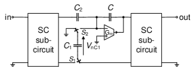
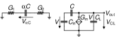
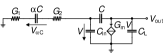
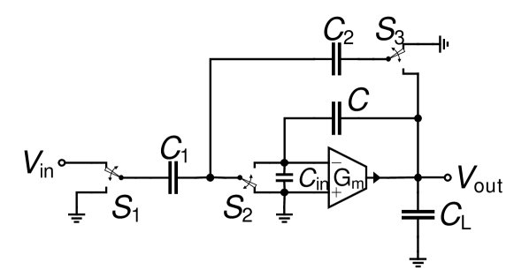
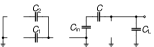
In this Section, we will recall the different noise mechanisms appearing in SC filters based on the stray-insensitive SC integrator shown in Fig. 1 as part of a larger SC filter. The integrator is made of an OTA having a transconductance , a feedback (or integrating) capacitor , a switched-capacitor and an eventual capacitor always connected to the virtual ground. It is assumed that this SC filter uses two non-overlapping phases and which allows for the switches to be represented by toggle switches as shown in Fig. 1. It is also assumed that the OTA is ideal (in particular has infinite voltage gain and zero offset voltage) and that the circuit fully settles in each phase ( and where is the equivalent capacitance accounting for the feedback). During each phase, the SC integrator operates as a continuous-time circuit. The noise is generated from the noise sources in the OTA and the switches. During the sampling phase (shown in Fig. 1(a)), the noise voltage across the sampling capacitor is sampled at the end of phase , freezing a noise charge on , which will be transferred to the integrating capacitor during the next phase . At the end of phase (shown in Fig. 1(b)), not all of the charge stored on are transferred to the integrating capacitor . Indeed, assuming that the OTA has infinite gain and has enough time to settle during phase , the voltage across at the end of phase should ideally be zero leaving no charge on . However, because of the noise voltages coming from the switches and the OTA, the voltage across at the end of phase is not zero, leaving some random charge on that are not transferred to . Because of charge conservation at the virtual ground node of the OTA, the random charge left on induces a random charge transfer error on capacitor . The noise charge sampled on at the end of phase and transferred to the integrating capacitor during phase and the charge transfer error on the integrating capacitor due to the noise voltage across at the end of phase , can be modeled by a noise charge injector as shown in Fig. 1(b), injecting a noise charge at the end of phase . The noise charges and are uncorrelated and the variance of the noise charge injected into the virtual ground is therefore the sum of the variances of the noise charge due to the different noise sources active in each phase (switches and OTAs) and sampled at the end of phases and
| (1) |
The variances of the injected noise charge and are calculated in each phase from the variances of the voltages and as
| (2) |
This noise charge is eventually shared with other capacitors connected in parallel to and then part of it is then propagating from the virtual ground where it was injected towards the filter output, resulting in a noise voltage at the output. The noise voltage variance at the filter output can be evaluated by first calculating the sampled-data -transfer function from the noise charge injected at the virtual ground to the output using the technique described in [6, 5]. This technique is general but quite cumbersome and we will show below that in some simple cases, it can also be calculated directly in the time domain using recursive relations.
According to 2, in order to calculate the noise charge variances, we need to compute the noise voltage variances across all the switched capacitors connected to the virtual ground of the integrator. This can be done by calculating the PSD of the noise voltage across the switched capacitors during each phase and integrating it over frequency. Obtaining these PSD requires to first derive the transfer functions from the noise sources (switches and OTAs) to the voltage across the switched capacitors. The noise voltage variances are finally obtained by integrating the PSD over frequency. All this process is actually a quite fastidious task. Alternatively, we can check whether the extended Bode theorem presented in Part I of this article may eventually be used to this purpose. Contrary to the SC amplifier and track & hold circuits discussed in Part I, in the case of SC filters, the voltage at the virtual ground of the OTA shown in Fig. 1 does not only depend on the output voltage but also on the voltages and .
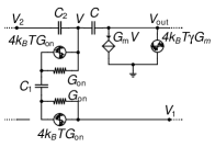
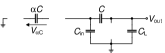
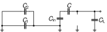
In order to calculate the effective virtual ground voltage , the integrator shown in Fig. 1, can be modelled by the equivalent linear circuit shown in Fig. 2(a). The switches are replaced by their on-conductance in parallel with their thermal noise current source having a PSD . The OTA is modelled by a voltage-controlled current source (VCCS) in parallel with its thermal noise current source having a PSD given by where is the OTA noise excess factor defined as where is the OTA input-referred thermal noise resistance. From the circuit of Fig. 2(a), the voltage at the virtual ground node can be expressed as
| (3) |
Assuming that the switch conductance is very large (more precisely that ), the transfer functions , and the feedback voltage gain can be assumed frequency-independent and are given by
| (4a) | ||||
| (4b) | ||||
| (4c) | ||||
where the approximations account for the fact that in SC filters, contrary to the cases of the SC amplifier and track & hold circuits analyzed in Part I, the integrator feedback capacitance is usually much larger than the switched and non-switched capacitances and (). Additionally, capacitors and connected to the virtual ground, have their other node connected either to the ground or to the output of another OTA. Hence, voltages , and in 3 are of the same order of magnitude and ultimately bounded by the supply voltage . Under the above assumptions, the two first terms in 3 can be neglected and 3 can be approximated by
| (5) |
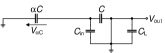
Using 5, the VCCS can now be replaced by a conductance of value leading to the equivalent circuit shown in Fig. 2(b). As in Part I, the latter circuit can be considered as a passive network and the extended Bode theorem can be used. The equation to calculate the thermal noise voltage variance between any node and of the SC filter is recalled here because it is central to the calculation method
| (6) |
Eq. 6 only requires the evaluation of the three capacitances , and . The latter can easily be calculated by inspection of the three equivalent circuits depicted in Fig. 3 which are each composed only of capacitors. The extended Bode theorem will now be illustrated and validated by transient noise simulations for various SC filters in the next Section.
III Practical Examples of Thermal Noise Estimation in SC Filters
SC filters operate periodically and each period corresponds to a succession of phases and, in each phase, the circuit corresponds to a continuous-time passive or OTA-based capacitive circuit. Hence, the variance of the noise charge held in each capacitor of the SC filter at the end of each phase can be estimated using either the original Bode theorem for passive circuits or the extended Bode theorem presented in the previous Section for OTA-based active SC filters. These thermal noise charges generated in different phases are uncorrelated in time. Thus, the total noise charge held on a capacitor after one switching period can be expressed as the sum of the noise charges generated in each phase. Unlike the SC amplifier and track & hold examples presented in Part I, where the capacitors are reset between two successive periods, in SC filters the capacitors (particularly the integrating capacitor) are not always reset. A recursive relation can then be established between the noise variance at the end of the present switching period and the previous ones.
For all the SC filters analyzed in this Section, it is assumed that the circuit operates with two non-overlapping phases and which allows for the switches to be represented by toggle switches. It is also assumed that the OTAs have infinite voltage gain, have no offset, are linear, don’t show any slew-rate and can therefore be represented by simple VCCS. It is also assumed that the time constants related to the switches are much smaller than half a period () and that the OTA output node fully settles within each phase. This requires the settling time to be much smaller than half the sampling period where and is the effective load capacitance with the feedback gain.
The validation of the thermal noise estimation method is performed by transient noise simulation using the ELDO© simulator [4]. The transient noise simulation technique is close to the physical noise behavior taking place in SC circuits and is quite easy to set up. It is also the most suitable for verifying the noise behavior through the phases and switching periods for the different simulated filters. The transient noise simulations are performed using ideal components, in particular the OTAs are modelled by simple VCCS with a thermal noise current source at the output having a PSD . In order to obtain reliable results, the simulator noise bandwidth is set to be higher than the maximum pole of all the transfer functions seen by any noise source in the circuit during any phase.
The validation starts with the passive first-order LP filter which noise voltage variances in each phase can actually be calculated by means of the original Bode theorem since it is a passive circuit. The second example is the basic stray-insensitive SC integrator which is the main building block for implementing higher order SC filters. Finally, the first-order active LP filter is analyzed.
III-A Passive First-order LP Filter
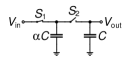


Fig. 4 shows the schematic of a passive first-order LP filter where the SC plays the role of the resistance of a simple first-order LP filter. The circuit is operated periodically in two phases. During phase , the input voltage is sampled on capacitor , while the voltage across is read out. During phase , the charge sampled on is then added to the charge already existing on and the total charge on and is then shared between and . The accumulation and averaging of charge occurring during phase translates into a recursive relation between the output and input voltages resulting in a transfer function in the -domain given by
| (7) |
For frequencies much smaller than the sampling frequency, this circuit operates as a first-order LP filter with a cutoff frequency given by
| (8) |
where is the sampling frequency.
The calculation of the output noise voltage variance is detailed below. During phase , the noise generated by the input switch S1 is first sampled on capacitor . The noise voltage variance across capacitor during phase can be calculated by applying the Bode theorem as explained in Part I with the capacitances and shown in Fig. 5 and resulting in
| (9) |
The noise charge frozen on capacitor at the end of phase can hence be expressed as
| (10) |
This charge is then shared between capacitors and during phase . At the end of phase , after the switch S2 has opened, only a fraction of the charge will remain on capacitor . Hence the variance of the noise charge generated during phase and remaining on capacitor at the end of phase is given by
| (11) |
To this charge generated during phase and left on during phase adds the charge sampled on at the end of phase due to the noise generated by the switch S2. This noise charge can be calculated directly using the Bode theorem with the capacitances and shown in Fig. 6 for phase resulting in
| (12) |
The corresponding noise charge sampled at the end of phase on capacitor and due to the noise generated by switch S2 simplifies to
| (13) |
The variance of the total noise charge injected on at the end of phase due to the noise generated during phase and phase is then given by
| (14) |
Capacitor is not reset between two consecutive periods. Hence, the noise charge generated during the two phases of a current period, which variance is calculated above, adds to the noise charge already held on capacitor and originated during the previous switching periods. Let be the noise charge held on capacitor at the end of the switching period. The latter charge is held on during phase of the next switching period and then shared between and at the beginning of phase . When switch S2 opens at the end of phase , a fraction of this charge will remain on . The variance of the total noise charge sampled in at the end of the switching period can then be expressed as
| (15) |
Since 15 is a recursive relation, the noise charge variance at the end of the period can be expressed as
| (16) |
After several switching periods, depending on the capacitors ratio, the second term in 16 tends to unity and the noise voltage variance seen across converges to
| (17) |
This result might seem trivial since it actually corresponds to the variance of the noise voltage of the equivalent continuous-time first-order LP filter! However, the continuous-time equivalent circuit of SC circuits does not always provide the correct thermal noise variance.
In order to validate the above noise estimation, the circuit is simulated with capacitors , as shown in Fig. 7(a). The output noise is calculated for the readout phase () when the output is floating and before the injection (), hence the calculated value remains constant for the entire period. The value of the capacitors chosen leads to a rapid convergence, it only takes periods. The transient noise simulation validates the noise estimation method for each period of sampling and confirms than the noise increases through the periods and converges to a constant value as predicted by the calculation based on the presented noise estimation method.
Fig. 7(b) shows a simulation with a different capacitance ratio chosen for a slower convergence in order to validate the noise convergence in detail. The recursive relation and the convergence of the output noise is confirmed by the perfect match of the simulated and calculated results. These calculations also agree with the results presented in [7].
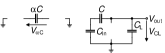
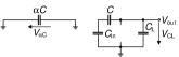
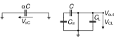
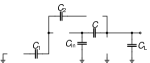
III-B The Integrator

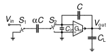
Fig. 8 shows the implementation of a non-inverting stray-insensitive SC integrator [1] where is the ratio between the sampling capacitance and the integrating capacitance . Each switching period of the SC integrator is composed of two non-overlapping phases. A charge is sampled on capacitor at the end of phase while the integrator output voltage is read by the next stage. This charge is then transferred to during phase and adds to the charge already held on from the previous period. The transfer function of this stage in the -domain is given by [1]
| (18) |
.
.
.

The goal is to calculate the variance of the thermal noise voltage at the output. During phase , the only capacitor sampling a noise charge is , since the other capacitances are holding their charge sampled in the previous period (except for the part that comes from the direct noise which will be accounted for when calculating the noise during phase ). The noise voltage variance across capacitor during phase is calculated using the extended Bode theorem 6 with the help of the schematics shown in Fig. 9 for the calculation of capacitances , and . Since the OTA is completely disconnected from the sampling capacitor during phase , it does not contribute to the noise sampled on capacitor at the end of phase . This is consistent with the values of the capacitances and extracted from the circuits of Fig. 9 which make the second and third terms of 6 due to the OTA zero. The variance of the noise voltage sampled on capacitor at the end of phase is then simply given by
| (19) |
The corresponding noise charge sampled at the end of phase and transferred to capacitor during phase is given by
| (20) |
At the end of phase , because of the noise coming from the switches S1 and S2 and from the OTA, not all the charge sampled on are transferred to and some will remain on after the opening of switch S2 leading to a random charge “deficit” on . The latter can be modelled by the charge which is equal to the charge sampled on at the end of phase . The variance of this charge can be calculated from the variance of the voltage across during phase which can be estimated by applying the extended Bode theorem 6 to capacitor during phase . Capacitances , and together with the feedback gain during phase are calculated with the help of the schematics shown in Fig. 10. The noise voltage variance across during phase is derived in details in Appendix V-A. Assuming that and (i.e. and ), leads to
| (21) |
where and . The corresponding variance of the noise charge sampled on at the end of phase is then given by
| (22) |
Both noise charges and add to the charge already held on capacitor . This noise charge injection on can be modeled by the charge injector defined by 1 and given by
| (23) |
To evaluate the output noise voltage variance, let’s first consider as the variance of the noise charge stored on capacitor at the end of the switching period. The noise charge variances calculated above will add to so that the total noise charge held on capacitor at the end of the switching period is given by
| (24) |
Eq. 24 shows that the sampled noise charge at the period is not shared with any other capacitor and is entirely added at the period to the noise charge already held on . Therefore the resulting sampled noise charge is the noise generated during a single period multiplied by the number of switching periods . The variance of the total noise charge cumulated on after switching periods, assuming , is then simply given by resulting in
| (25) |
The corresponding variance of the noise voltage at the OTA output after switching periods is then given by
| (26) |
As expected for an integrator, 26 shows that the output noise voltage variance increases proportionally with the switching periods , which is typical of a Wiener process [8].
Eq. 26 does not account for the direct noise at the output of the OTA which would be sampled by the next stage at the end of phase . The latter adds to the sampled noise given by 26. It can be calculated by applying the extended Bode theorem 6 applied on the load capacitor during the readout phase . The derivation is detailed in Appendix V-B. Assuming again that and , it results in
| (27) |
Finally the total output noise voltage variance during the readout phase is given by
| (28) |
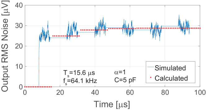
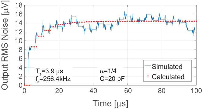
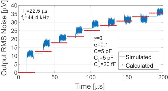
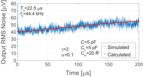
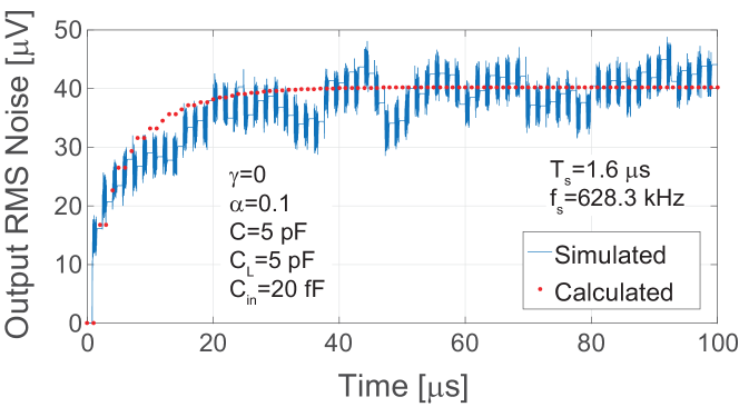
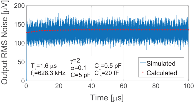
Eq. 28 has been verified using transient noise simulations. Fig. 11(a) shows the transient simulation of the output RMS noise voltage in the case of a noiseless OTA (i.e. ) compared to the calculated noise voltage using (28). Note that the calculated noise corresponds to the simulated noise for the readout phase during which the output voltage remains constant since the OTA does not generate any direct noise during this phase when is set to zero.
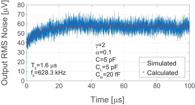
Fig. 11(b) presents the simulation for an OTA with a noise excess factor generating the additional direct noise during the readout phase having an RMS value of . Both simulations show the increase of the output RMS noise voltage following a law. Fig. 11 shows that the simulations precisely match the RMS output noise voltage calculated from 28. The excellent fit between the calculated and simulated noise confirms the effectiveness of the proposed noise calculation method.
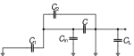
III-C Active First-order LP Filter Based on OTA
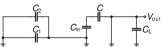
The active SC LP filter is implemented using an OTA as shown in Fig. 12. The input signal is sampled by capacitor during phase while capacitor is discharged and capacitor holds the charge transferred during the previous period. The charge sampled on at the end of phase is then transferred to and during phase . The transfer function of this filter in the domain is given by
| (29) |
where and . Usually and are much smaller than unity to set the cut-off frequency at a much smaller value than the sampling frequency. In order to further simplify the calculations, the ratios can be assumed equal and much smaller than unity, . For frequencies much smaller than the sampling frequency, this circuit operates as first-order LP filter with a cutoff frequency given by
| (30) |
where is the sampling frequency.
In this example, the readout of the output voltage is performed at the end of phase . Therefore, the output noise is composed of the noise sampled on the integrating capacitor at the end of phase of the previous switching period and held over to phase of the next switching period, and the direct output noise sampled on at the end of phase and originating from the OTA during this readout phase . Hence, the noise calculation starts with the evaluation of the total noise sampled on the integrating capacitor and coming from phase and phase , and follows with the estimation of the direct noise sampled at the end of phase .
.
.
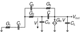

At the end of phase , capacitors and sample a noise charge generated by switches S1, S2 and S3. The sum of these noise charges is then injected into the virtual ground and transferred to the feedback capacitors and during the charge transfer phase . The noise voltage variances across capacitors and during phase can be calculated applying the extended Bode theorem 6 with the use of the schematics shown in Fig. 13 resulting in
| (31a) | ||||
| (31b) | ||||
The corresponding noise charge sampled during phase and injected into the virtual ground during phase is given by
| (32) |
This noise charge is then shared by the parallel capacitors and during phase . Consequently, only a fraction of this charge will remain on capacitor after the end of phase when capacitor is disconnected from . Hence, the variance of the noise charge generated during phase and remaining on after the end of phase is given by
| (33) |
where .
The noise charge that is injected into the virtual ground at the end of phase actually corresponds to the noise charge that is sampled on the integrating capacitor when capacitors and are disconnected from the virtual ground and the output node, respectively. The variance of this noise charge is calculated from the variance of the noise voltage across capacitor at the end of phase due to the noise of the switches and OTA generated during phase . The latter is derived using the extended Bode theorem 6 in Appendix V-C. It can be written separating the contributions of the switches and OTA as
| (34) |
where and are given by 55 and 54, respectively. For and , and reduce to
| (35a) | ||||
| (35b) | ||||
with . The corresponding noise charge variance sampled and remaining on at the end of phase (ignoring the noise charge coming from phase ) is expressed as
| (36) |
The variance of the total noise charge injected into capacitor at the end of phase due to the noise generated during phases and is then given by
| (37) |
where
| (38a) | ||||
| (38b) | ||||
Similarly to the passive first-order SC filter discussed above, capacitor is not reset and will cumulate part of this injected noise charge. During the switching period, the noise charge , which variance is calculated above, will add to the noise charge already present on capacitor at the end of the switching period . The charge is shared between capacitors and during phase of the switching period , and when capacitor is disconnected from at the end of phase , only a fraction of this charge will remain on . The variance of the total noise charge sampled on at the end of the switching period can therefore be expressed as
| (39) |
Eq. 39 corresponds to a recurrence equation similar to the example of the passive SC LP filter. The variance of the noise charge held on capacitor at the switching period can hence be expressed as
| (40) |
where
| (41) |
After several switching periods the right term of 40 tends to unity. Hence, the variance of the noise voltage sampled on capacitor tends to the value
| (42) |
where and with , and given by
| (43a) | ||||
| (43b) | ||||
| (43c) | ||||
Since the output voltage is read (or sampled) at the end of phase , the direct noise that appears at the OTA output during this readout phase adds to the sampled noise 42. The variance of this direct output noise voltage can also be calculated using the extended Bode theorem 6. The derivation of capacitances , and can be done with the help of the schematics of Fig. 13 but applied to the load capacitor . The feedback gain during phase which is also required in 6, is . The variance of the output voltage during phase therefore reduces to
| (44) |
where .
The total output noise voltage variance is then simply given by summing 42 and 44 resulting in
| (45) |
In case can be assumed to be much larger than and (i.e. and ), then and the noise contribution of the OTA to the sampled noise can be neglected (i.e. ) and 45 reduces to
| (46) |
| (54) |
| (55) |
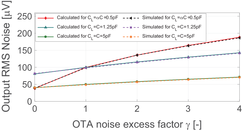
In order to validate the above results, the circuit is simulated for different values of capacitors and noise excess factor. Fig. 15(a) shows the transient behavior of the output RMS noise for , , and a noiseless OTA () resulting in an output RMS noise voltage at . Note that the simulated noise during phase is constant because the direct noise is not present in this phase when the OTA is considered noiseless. The simulations in Figs. 15(b) and 15(c) take into account the noise originated from the OTA with and different values of the load capacitance. The simulations show a direct noise but the value is not the same during both phases because the continuous-time circuit for each phase is different. The expression in 45 is the noise calculated during phase and it is slightly higher than the noise during phase . This can be specially observed in Fig. 15(c) due to the small load capacitor which increases the direct noise during phase compared to .
The excellent match between the transient noise simulations and the results calculated from 45 and presented in Fig. 15 demonstrates the efficiency of the proposed noise estimation method in accurately predicting the value of the noise variance as well as how exactly the output noise converges to its steady-state value.
IV Conclusion
The design of low-noise SC filters often comes at the cost of higher power consumption. The optimization of SC filters for achieving at the same time low-noise operation at low-power therefore requires an accurate estimation of the integrated noise at the filter output. In Part I of this paper, we have shown how the original Bode theorem can be extended to active SC circuits using OTAs with capacitive feedback. This generalization allows the calculation of the thermal noise voltage variance across each capacitor of the circuit by simple inspection of several equivalent schematics made of capacitors only, avoiding the evaluation of complex transfer functions and cumbersome integrals. This Part II presents how the extended Bode theorem can also be applied to SC filters built with OTAs. It is illustrated by three examples, including a passive first-order LP filter (which actually can be calculated with the original Bode theorem), the basic stray-insensitive integrator and finally an active first-order LP filter. The analytical results obtained from the extend Bode theorem are successfully validated using transient noise simulations. The simulations results are very close to the analytical expressions demonstrating the effectiveness of the proposed method also for SC filters based on OTAs.
V Appendix
V-A Integrator - Derivation of
The variance of the noise voltage across at the end of phase can be evaluated using the extended Bode theorem 6 with the help of the schematics of Fig. 10 for the evaluation of , and and of the feedback gain given by
| (47) |
where . This leads to
| (48) |
where . Usually and can be considered much smaller than (i.e. and ) leading to
| (49) |
V-B Integrator - Derivation of direct noise
V-C OTA-based LP active filter - Derivation of
The variance of the noise voltage across at the end of phase can be calculated using the extended Bode theorem 6. Capacitances , and are calculated with the help of Fig. 14. Eq. 6 also requires the feedback gain during phase which for is given by
| (52) |
Applying the extended Bode theorem 6 and separating the contribution of the OTA and the switches leads to
| (53) |
where and are given by 54 and 55, respectively. For and , 54 and 55 reduce to
| (56a) | ||||
| (56b) | ||||
References
- [1] R. Gregorian and G. C. Temes, Analog MOS Integrated Circuits for Signal Processing. Wiley, 1986.
- [2] R. Schreier, J. Silva, J. Steensgaard, and G. C. Temes, “Design-oriented Estimation of Thermal Noise in Switched-capacitor Circuits,” IEEE Transactions on Circuits and Systems I: Regular Papers, vol. 52, no. 11, pp. 2358–2368, Nov. 2005.
- [3] J. Goette and C. A. Gobet, “Exact Noise Analysis of SC Circuits and an Approximate Computer Implementation,” IEEE Trans. on Circuits and Systems, vol. 36, no. 4, pp. 508–521, April 1989.
- [4] P. Bolcato and R. Poujois, “A New Approach for Noise Simulation in Transient Analysis,” in Proc. of the IEEE International Symposium on Circuits and Systems (ISCAS), vol. 2, May 1992, pp. 887–890.
- [5] C. Enz, F. Krummenacher, and A. Boukhayma, “Simple Thermal Noise Estimation of OTA-based Switched-capacitor Filters,” in 2015 International Conference on Noise and Fluctuations (ICNF), June 2015, pp. 1–4.
- [6] B. Furrer, “Rauschen von Filtern mit geschalteten Kapazitäten,” PhD, ETHZ, Date 1983, no. 7284.
- [7] A. Boukhayma and C. Enz, “A New Method for kTC Noise Analysis in Periodic Passive Switched-capacitor Networks,” in 2015 IEEE 13th International New Circuits and Systems Conference (NEWCAS), June 2015, pp. 1–4.
- [8] A. Papoulis, Probability, Random Variables and Stochastic Processes, 1st ed. New York: Mc Graw-Hill, 1981.
![[Uncaptioned image]](/html/1908.08109/assets/x44.png) |
Christian Enz (M’84, S’12) received the M.S. and Ph.D. degrees in Electrical Engineering from the EPFL in 1984 and 1989 respectively. He is currently Professor at EPFL, Director of the Institute of Microengineering and head of the IC Lab. Until April 2013 he was VP at the Swiss Center for Electronics and Microtechnology (CSEM) in Neuchâtel, Switzerland where he was heading the Integrated and Wireless Systems Division. Prior to joining CSEM, he was Principal Senior Engineer at Conexant (formerly Rockwell Semiconductor Systems), Newport Beach, CA, where he was responsible for the modeling and characterization of MOS transistors for RF applications. His technical interests and expertise are in the field of ultralow-power analog and RF IC design, wireless sensor networks and semiconductor device modeling. Together with E. Vittoz and F. Krummenacher he is the developer of the EKV MOS transistor model. He is the author and co-author of more than 250 scientific papers and has contributed to numerous conference presentations and advanced engineering courses. He is an individual member of the Swiss Academy of Engineering Sciences (SATW). He has been an elected member of the IEEE Solid-State Circuits Society (SSCS) AdCom from 2012 to 2014. He is also the Chair of the IEEE SSCS Chapter of Switzerland. |
![[Uncaptioned image]](/html/1908.08109/assets/x45.png) |
Sammy Cerida Rengifo received the B.S. degree, with honors, in electrical engineering from Pontifical Catholic University of Peru (PUCP) in 2014. He obtained the M.S. joint degree in Micro and Nanotechnologies for Integrated Systems (Master Nanotech) between Politecnico di Torino, Grenoble INP, and EPFL. His master thesis research was carried out at EM Microelectronic-Marin, Neuchâtel, Switzerland, on the investigation and analysis of next-generation UHF RFID tags. In 2017, he joined the CSEM in Neuchâtel, where he is currently working towards his PhD in the field of ultra low-power radars. |
![[Uncaptioned image]](/html/1908.08109/assets/x46.png) |
Assim Boukhayma received the graduate engineering degree (D.I.) in information and communication technology and the M.Sc. in microelectronics and embedded systems architecture from Institut Mines Telecom (IMT Atlantique), France, in 2013. He was awarded with the graduate research fellowship for doctoral studies from the French atomic energy commission (CEA) and the French ministry of defense (DGA). He received the Ph.D. from EPFL in 2016 on the topic of Ultra Low Noise CMOS Image Sensors. In 2017, he was awarded the Springer Theses prize in recognition of outstanding Ph.D. research. He is currently a scientist at EPFL ICLAB, conducting research in the areas of image sensors and noise in circuits and systems. From 2012 to 2015, he worked as a researcher at Commissariat a l’Energie Atomique (CEA-LETI), Grenoble, France. From 2011 to 2012, he worked with Bouygues-Telecom as a Telecommunication Radio Junior Engineer. |
![[Uncaptioned image]](/html/1908.08109/assets/x47.png) |
François Krummenacher received the M.S. and Ph.D. degrees in electrical engineering from the Swiss Federal Institute of Technology (EPFL) in 1979 and 1985 respectively. He has been with the Electronics Laboratory of EPFL since 1979, working in the field of low-power analog and mixed analog/digital CMOS IC design, as well as in deep sub-micron and high-voltage MOSFET device compact modeling. Dr. Krummenacher is the author or co-author of more than 120 scientific publications in these fields. Since 1989 he has also been working as an independent consultant, providing scientific and technical expertise in IC design to numerous local and international industries and research labs. |