Simple Thermal Noise Estimation of Switched Capacitor Circuits Based on OTAs – Part I: Amplifiers with Capacitive Feedback
Abstract
This paper presents a simple method for estimating the thermal noise voltage variance in passive and active switched-capacitor (SC) circuits using operational transconductance amplifiers (OTA). The proposed method is based on the Bode theorem for passive network which is extended to active circuits based on OTAs with capacitive feedback. It allows for a precise estimation of the thermal noise voltage variance by simple inspection of three equivalent circuits avoiding the calculation of any transfer functions nor integrals. In this Part I, the method is applied to SC amplifiers and track & hold circuits and successfully validated by means of transient noise simulations. Part II extends the application of the method to integrators and active SC filters.
Index Terms:
thermal noise, kTC, Bode theorem, amplifier.I Introduction
Switched-capacitor (SC) circuits were invented in the 70’s as a way to perform analog signal processing on-chip using the capacitors, switches and amplifiers available in MOS technologies [1, 2]. They take advantage of the fact that the circuit characteristic only depends on capacitance ratios which turn out to be very accurate tanks to the excellent matching of capacitors. Additionally the frequency response of SC filters can be tuned by changing the clock frequency [3]. SC circuits have then been used broadly for various circuits including analog-to-digital and digital-to-analog converters [4]. They are increasingly used in many more applications like radio frequency (RF) circuits [5, 6, 7] or sensor front-end circuits [8, 9, 10] to perform various analog signal processing operations such as sampling, amplification or filtering.
The analysis of SC circuits has received considerable attention in the 80s’ in particular for the computation of the noise [11, 12, 13, 14, 15, 16, 17]. With the application of SC circuits to a wider range of analog and RF circuits, new computation techniques have also been proposed more recently [18, 19, 20]. Today, modern circuit simulators allow to compute noise for example in the time domain using transient noise analysis [21]. However all of these techniques remain complex and are mostly focused on an efficient numerical computation of the PSD by dedicated EDA tools. They cannot be used for the derivation of simple analytical expressions of the noise voltage variance.
The performance of SC circuits is ultimately limited by the thermal and flicker noise (or noise) generated by the amplifiers and by the thermal noise coming from the switches. Since SC circuits are sampled-data systems, the broadband thermal noise is aliased into the Nyquist band, resulting in an increase of the noise power spectral density (PSD) by a factor equal to the ratio of the equivalent noise bandwidth to the Nyquist frequency which is usually much larger than one [22, 14, 23]. The noise contribution can therefore usually be neglected and if it still remains important, the amplifier noise and offset can be reduced by increasing the transistor gate areas or eventually eliminated thanks to circuit techniques like auto-zeroing [24, 25, 26, 23] or chopper stabilization [27, 28, 23]. Under such conditions, the sampled thermal noise remains the dominant noise source particularly when minimal capacitance values are used, since the sampled noise voltage variance is inversely proportional to the capacitance.
Since the power consumption and silicon area are proportional to the capacitance [29], whereas the noise voltage variance is inversely proportional to the capacitance, it is crucial to identify which capacitances are setting the noise voltage variance. Unfortunately, the derivation of the noise PSD and variance is not easy because SC circuits are periodically time-varying circuits. The noise is therefore cyclostationary and usually characterized by the power spectral density (PSD) averaged over one period [30].
The optimization of SC circuits for achieving at the same time low-noise operation at low-power requires an accurate estimation of the noise variance. The latter is traditionally calculated for each phase in the frequency domain by first evaluating the transfer functions from all the noise sources to the node where the noise needs to be evaluated. The total noise PSD is then integrated over frequency to provide the noise variance. This approach is however quite tedious and impractical [31] and for large networks, it becomes extremely cumbersome to get an analytical expressions [32].
This work proposes a simple method for estimating the thermal noise voltage variance at any port of passive and active circuits made of operational transconductance amplifiers (OTA) with capacitive feedback as found in SC circuits [33]. The proposed method, based on the Bode theorem [34], allows the calculation of the thermal noise voltage variance across any capacitor by simple inspection of several equivalent schematics made of capacitors only, avoiding the evaluation of complex transfer functions and cumbersome integrals.
Part I is dedicated to the derivation of the extended Bode theorem and its application to SC amplifiers and track & hold circuits. Part II is focused on the application of the extended Bode theorem to SC filters. Section II of this first Part starts by recalling the Bode theorem, which is at the heart of the proposed method. Section III then presents an extension of this theorem to OTAs with capacitive feedback as found in SC circuits. The method is then illustrated in Section IV by two simple examples, namely a SC amplifier and a SC track & hold circuit. The calculated noise in each case is compared to transient noise simulations results showing an excellent match. Conclusions are then given in Section V
II The Bode Theorem for Passive Networks
The Bode theorem [34, 35, 36] is a very efficient method to calculate the noise voltage variance at any port of an circuit and particularly of capacitive networks. However, this method is limited to passive networks.
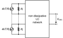

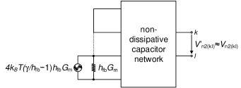
In linear circuits, the noise analysis is traditionally performed by integrating the noise PSD. This requires the calculation of the transfer functions from each uncorrelated noise source to the node where the noise has to be evaluated (for example at the circuit output) and then adding the obtained uncorrelated contributions. In case of a passive network, the thermal noise is generated in the resistors while the rest of the circuit made of ideal capacitors and inductors is noiseless. The circuit can then be represented as shown in Fig. 1(a) where all resistors are modeled by a noiseless resistor in parallel with a noisy current source with power spectral density . The thermal noise variance between any nodes and of the passive circuit can be calculated using the Bode theorem without the need for computing any integral by simple inspection of two equivalent circuits. The thermal noise voltage variance at any port is simply given by [34, 35, 36]
| (1) |
where is the Boltzmann constant and the absolute temperature. Capacitance is defined as
| (2) |
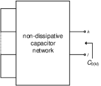
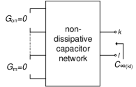
which corresponds to the capacitance obtained when looking into the port after having removed all resistances from the circuit (or set them to infinity) as illustrated in Fig. 1(b). Capacitance is defined as
| (3) |
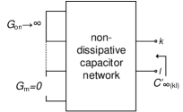
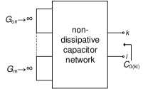
which corresponds to the capacitance obtained when looking into the port after having replaced all resistances by a short circuit (or set them to zero) as illustrated in Fig. 1(c).
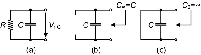
The simplest example of the application of the Bode theorem to a passive circuit is the 1st-order low-pass filter illustrated in Fig. 2a. As shown in Fig. 2b, capacitance is obtained after removing the resistance and is therefore equal to . Capacitance is obtained from 3 after replacing the resistance by a short resulting in . Applying the Bode theorem 1, the noise voltage variance is then simply equal to the well-known formula .
III Extension of the Bode Theorem to Transconductance Amplifiers with Capacitive Feedback
This Section presents an extension of the Bode theorem to be used for calculating the thermal noise voltage variance seen at any port of an OTA-based SC circuit during a given phase.
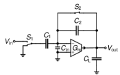
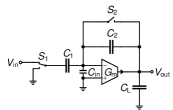
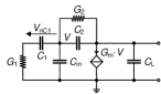
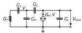
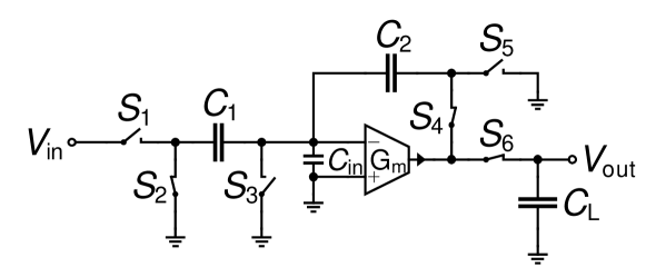
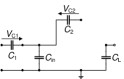
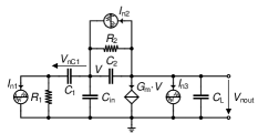
The Bode theorem presented above strictly applies only for the calculation of the thermal noise voltage variances of passive networks. However, it will be shown below that it can be extended to estimate the thermal noise voltage variance of amplifiers implemented with transconductance stages having a capacitive feedback. The simplest of such amplifier is the capacitive feedback amplifier shown in Fig. 3, where the amplifier is a differential OTA [3, 37]. Note that the amplifier can also represent a single-ended transconductance stage as simple as a single transistor or cascoded transistor for improved dc gain [38]. For more power-efficient implementation, the single-ended amplifier can be implemented by a simple inverter to take advantage of its current reuse feature [39]. In the following discussion, the OTA is assumed to be ideal (infinite DC gain, offset free, no saturation) and can be modelled by a voltage controlled current source (VCCS).
The amplifier operates with two non overlapping phases: the autozero (AZ) phase , followed by the amplification phase . During phase , shown in Fig. 3(a), the amplifier output is connected to its input, discharging the feedback capacitor . Assuming the DC gain of the OTA is infinite, capacitors and are then also discharged. In the amplification phase , switch is connected to the input, amplifying the input voltage. The voltage gain between the input and output voltage is simply equal to . Note that this amplifier is called autozero amplifier because it strongly reduces the OTA offset and flicker noise [23]. It can be shown that the residual input-referred offset of the amplifier is equal to the OTA original offset divided by the amplifier voltage gain (assuming again that the OTA has an infinite DC gain). It can also be shown that the amplifier equivalent input-referred noise is free from the original OTA flicker noise and increased due to the aliasing of the broadband thermal noise due to the sampling process [23].
We are interested in the output noise variance at the end of the amplification phase , when the signal is actually read at the output. As mentioned above, thanks to the AZ process, the flicker noise of the OTA is strongly reduced [23] and hence the noise at the amplifier output during phase is dominated by the thermal noise coming from the OTA and from the switches. The noise voltage variance at the output can be calculated in a classical way by integrating the output noise voltage PSD over frequency or calculating the equivalent noise bandwidth. An additional noise component needs to be accounted for at the end of phase , namely the noise that is generated across capacitor during phase . This noise is sampled as a noise charge on when the switch S1 opens at the end of phase and then transferred to the feedback capacitor during phase . The variance of this output noise voltage is obtained by first calculating the variance of the noise voltage across during phase by calculating the noise voltage PSD across and integrating it over frequency. This noise voltage variance corresponds to a frozen charge that is then transferred to the feedback capacitor during phase . Assuming that the OTA DC gain is infinite, the voltage across is equal to the output voltage. The output noise voltage variance due to the noise sampled on at the end of phase is simply equal to the noise voltage variance across multiplied by the square of the voltage gain . Now, although the procedure is straightforward, it is actually not always possible to get simple analytical expressions for the noise voltage variances mentioned above. Of course the latter can always be calculated numerically using a simple .NOISE simulation, but for circuit optimization it is useful to have analytical expressions showing the dependence of the noise to the various components. The Bode theorem can unfortunately not be used because we now have an active component. However, we will show below that the noise voltage variances can be estimated by extending the original Bode theorem to circuits including amplifiers implemented as transconductance amplifiers with a capacitive feedback.
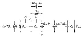
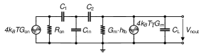
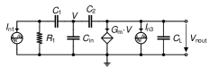
For the noise analysis, it is reasonable to use a small-signal analysis. The small-signal equivalent circuit of the amplifier of Fig. 3 used to calculate the output noise voltage is shown in Fig. 4, where the noise current sources across resistances represent the thermal noise of the switches having a PSD , where , whereas the noise current source across the VCCS represents the OTA thermal noise referred to the output with a PSD , where is the thermal noise excess factor close to unity for a single transistor and usually larger than 2 for a differential OTA.
In both phases and , neglecting the current noise sources, the voltage at the transconductance amplifier virtual ground is only a function of the output voltage
| (4) |
where is the feedback voltage gain. During phase it is simply equal to unity, whereas during phase it is given by
| (5) |
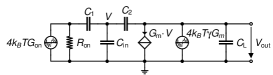
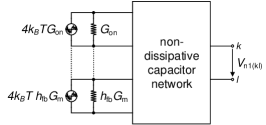
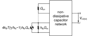
The circuits of Fig. 4 can therefore be simplified by replacing the VCCS by a simple resistance having a conductance equal to resulting in the simplified circuits shown in Fig. 5. The later circuits can now be considered as passive and can be represented as in Fig. 6(a). However, the Bode theorem cannot be applied directly because the noise current source corresponding to the conductance is not equal to like for the noise sources associated to the switch resistances. In order to apply the Bode theorem, the OTA noise current source PSD can be split into the sum of and a term that includes the OTA thermal noise excess. The circuit of Fig. 6(a) can hence be decomposed into two circuits, the circuit shown in Fig. 6(b), where all the conductances have the same noise temperature , and the circuit of Fig. 6(c), where the switches are considered noiseless and the noise source corresponding to conductance is considered to have a noise temperature equal to . The variance of the noise voltage between any node and of the circuit of Fig. 6(a) can then be calculated using the superposition of the noise sources as the sum of the noise voltage variance of the circuit shown in Fig. 6(b), where all the conductances have the same noise temperature , and noise voltage variance of the circuit shown in Fig. 6(c), corresponding to the excess noise in the equivalent conductance of the OTA with a noise temperature
| (6) |
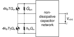
The Bode theorem for passive networks can then be applied to the circuit shown in Fig. 6(b) to calculate the noise voltage variance as
| (7) |
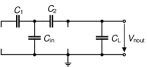
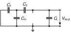
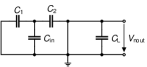
where corresponds to the capacitance seen when looking between the nodes and when all the switches and transconductance amplifiers are removed, and corresponds to the capacitance obtained looking between the nodes and when the switches are replaced by short-circuits and all OTAs have their output shorted to ground.
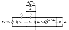
The circuit of Fig. 6(c) can be further simplified considering that usually and hence the on-conductances of the switches can be replaced by short-circuits resulting in the circuit shown in Fig. 6(d). The noise voltage variance accounting for the OTA excess noise temperature can therefore be estimated by applying the Bode theorem to the circuit of Fig. 6(d) resulting in
| (8) |
where corresponds to the capacitance seen between the nodes and when all the switches are replaced by short-circuits and the transconductance amplifiers are removed.
The total thermal noise voltage variance seen between nodes and is then given by summing 7 and 8, resulting in
| (9) |
Eq. 9 is central to this calculation method. It shows that the computation of , for example at the amplifier output, only requires the evaluation of the three capacitances , and . The latter can easily be calculated by inspection of the three equivalent circuits depicted in Fig. 7 which are each composed only of capacitors.
The extension of the Bode theorem presented in this Section will now be illustrated and validated by transient noise simulations for various SC circuits in the next Section.
IV Practical examples of thermal noise estimation in OTA-based SC circuits
IV-A SC Amplifier
IV-A1 Analysis
Let’s now get back to the SC amplifier shown in Fig. 3 and apply the extended Bode theorem to calculate the noise voltage variances. We start calculating the noise voltage variance across the sampling capacitor during phase . To this purpose, we need to calculate the three capacitances seen across , namely , and during phase . They can easily be calculated from the equivalent circuits shown in Fig. 8, resulting in
| (10a) | ||||
| (10b) | ||||
| (10c) | ||||
Recognizing that the feedback gain during phase is simply equal to unity, the noise voltage variance across during phase can be evaluated from 9 as
| (11) |
Eq. 11 is actually identical to the result derived analytically in Appendix VI-A by calculating the noise contributions from each of the noise sources shown in Fig. 4(a), namely the two switches and the OTA. Each contribution is obtained by first calculating the transfer function from each noise source to the voltage across capacitor and integrating the corresponding noise PSD over frequency. The noise voltage variances due to each of the noise source assuming that the switch resistances are negligible compared to (i.e. ) are given in Table II. The total noise voltage variance is obtained by summing these three variances resulting in the result shown in the last row of Table II which is identical to 11. Note that when setting in 11, we also get the same result than found in [40] which has been computed using the equivalent noise bandwidth approach. As expected, 11 does not depend on since the later is short-circuited. This happens even though the individual contributions of each switch depends on as shown in Table II, but their sum does not depend on anymore.
To this noise voltage variance corresponds a noise charge sampled on at the end of phase and having a variance
| (12) |
This charge is then injected to the virtual ground at the beginning of phase and transferred to the feedback capacitor during phase thanks to the action of the OTA. Assuming that the latter has an infinite DC gain and a zero offset voltage, the output voltage is equal to the voltage across . The output noise voltage variance due to the noise sampled on at the end of phase is then given by
| (13) |

.
.
.
.
.
.
The variance of the output noise voltage during phase is simply evaluated using 9 which requires the calculation of the three capacitances , and seen from the output. The later can be calculated from the equivalent schematics shown in Fig. 9 resulting in
| (14a) | ||||
| (14b) | ||||
| (14c) | ||||
Eq. 9 also requires the feedback gain which during phase is given by
| (15) |
The output noise voltage variance during phase can now be evaluated from 9 leading to
| (16) |
where
| (17a) | ||||
| (17b) | ||||
with
| (18) |
Note that 16 is identical to the result derived in Appendix VI-A using the classical approach described above and given in the last row of Table IV.
Before calculating the total noise voltage variance at the output, we can rewrite 13 as
| (21) |
where
| (22a) | ||||
| (22b) | ||||
The total output noise voltage variance at the end of phase is then given by summing 21 and 16, resulting in
| (23) |
where
| (24a) | ||||
| (24b) | ||||
It can be shown that the effect of is negligible as long as the DC gain of the OTA is infinite. The switch contribution given by 24b can be further simplified by setting (or ) resulting in
| (25) |
IV-A2 Simulations
The above results for the SC amplifier have been verified by transient noise simulation [21] in ELDO©. The simulations are performed on a circuit where the OTA is modeled by a simple VCCS and the switches are modelled by an ideal switch in series with a noisy resistor of resistance . The noise of the OTA is generated by a noisy resistor of value and injected at the OTA output by means of a VCCS with a unity transconductance. The sampling period has been chosen equal to and the temperature is set to .
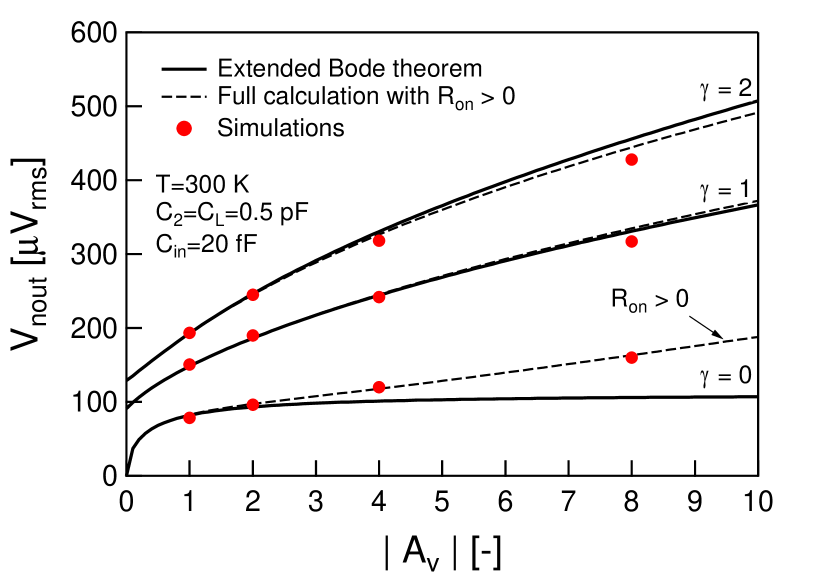
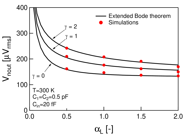
Fig. 10 shows the output noise rms voltage versus the gain for different values of the OTA excess noise factor . The simulations have been performed for different gains by changing the value of keeping . When increasing capacitance , it also increases the effective load capacitance with and the settling time where . The VCCS transconductance has therefore been chosen to keep a constant settling time for each values of and hence of . Note that the influence of the input capacitance is negligible and the later has been set to a realistic value of . The simulation results for and are very close to the estimation computed from 23. However, a small deviation is observed for the case where which corresponds to the noise generated by the switches only. The simulation results are slightly larger than the values predicted by 23, particularly for the maximum gain . The reason for this is that larger gains require larger resulting in the product increasing to about 0.27 which does no more fulfill the assumption of used in the Bode theorem derivation. The impact of a non-zero has been checked using the full analytical expressions obtained from the classical analysis detailed in Appendix VI-A111Note that, for the sake of compactness, the analytical expressions including the effect of a non-zero could not be included in the Appendix VI-A because they are rather large expressions.. The results are plotted in Fig. 10 by dashed lines which are very close to the simulation results, confirming the origin of the deviation.
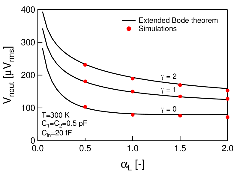
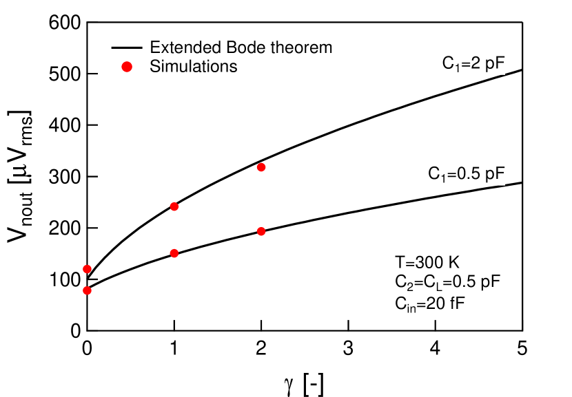
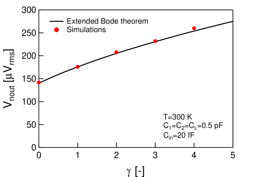
Fig. 11 shows the output noise rms voltage versus for and for a unity voltage gain (). The noise simulation results are very close to the estimation using 23.
IV-B SC Track & hold
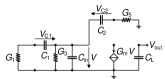
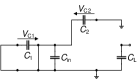
Fig. 13 shows the schematic of a basic SC track & hold (TH) circuit which can operate either as a TH or as a SC amplifier featuring a voltage gain set by the capacitance ratio . This circuit operates in two phases as shown in Fig. 13. During phase , shown in Fig. 13(a), the sampling capacitor samples the input signal . During this phase, the feedback capacitor is shorted to be reset, while the capacitor holds the charge that has been sampled at the end of phase of the previous switching period. During phase , shown in Fig. 13(b), the charge sampled in is transferred to the feedback capacitor . The output voltage seen across is then simply equal to . This voltage is then sampled and held on at the end of phase .

IV-B1 Analysis
The output voltage is read during phase from the hold capacitor and the sampled output noise must therefore be calculated at the end of phase . As in the example above, this circuit presents two non-overlapping phases for which the equivalent linear circuits are depicted in Fig. 14(a) and Fig. 15(a), respectively.
The capacitors sampling a noise charge at the end of phase are , as well as the parasitic capacitance at the OTA input . The sum of these noise charges is injected into the virtual ground during phase and transferred to the feedback capacitor . This noise charge on capacitor results in a noise voltage at the OTA output which will be sampled on at the end of phase .
, and .
.

.

.

The extended Bode theorem is used to calculate the noise voltage variances across capacitors , and for phase . The calculations of capacitors , and for each capacitor , and during phase is done using the equivalent circuits shown in Fig. 14. The resulting voltage variances based on 9 are then given by
| (26a) | ||||
| (26b) | ||||
| (26c) | ||||
The total noise charge generated during phase and injected into the virtual ground is then given by
| (27) |
The charge is subsequently transferred to capacitor during phase . Assuming again that the OTA has an infinite DC gain and a zero offset voltage, the output voltage is equal to the voltage across and the variance of the noise voltage seen at the output of the OTA resulting from this charge is hence given by
| (28) |
where
| (29) |
with , .
For phase , the noise charge held on capacitor can be directly calculated using the extended Bode theorem applied at the output. Fig. 15 shows the equivalent circuit schematics used for the noise voltage variance calculation using 9, which additionally also requires the feedback gain given by
| (30) |
The variance of the noise voltage generated across during phase is then given by
| (31) |
where
| (32a) | ||||
| (32b) | ||||
where is given by 19c and . The first term in 31 corresponds to the contribution of the OTA during phase and is actually identical to the expression 19a obtained for the SC amplifier. This not surprising since, assuming the inputs are grounded and the switches are ideal (zero resistance and hence noiseless), the circuit of Fig. 13(b) is identical to that of the SC amplifier shown in Fig. 3(a). The second term in 31 corresponds to the contribution of the switches.
In this circuit, none of the capacitors is holding a noise charge from one switching period to the next. Indeed, capacitor is reset during phase , capacitors and are reset during phase by the action of the OTA, while capacitor is connected to the OTA output during phase to sample the new value. Consequently, at the end of each switching period, the noise variance of the output voltage corresponds to the sum of the noise injected from phases and without any contributions from the previous switching periods. The variance of the total noise voltage sampled on can hence be expressed as
| (33) |
where
| (34a) | ||||
| (34b) | ||||
The first term in brackets of 33 is the noise contribution coming from the OTA, which only contributes during phase , while the second term is due to the noise coming from the switches during phases and . Note that 33 matches the result presented in [41] except for the second term in 34b which corresponds to the contribution of the switches in phase and which is omitted in [41]. This is reasonable since this term is usually small and can be neglected for the TH circuit because in general ().
IV-B2 Simulations
The results obtained for the SC TH have also been validated by transient noise simulation for a gain with the same sampling period and temperature as for the SC amplifier. The output noise rms voltage is plotted versus in Fig. 16 for 3 different values of . Fig. 17 shows the output rms noise voltage versus the OTA thermal noise excess factor for . In both cases, the simulation results are very close to the theoretical results predicted from the extended Bode theorem 23.
V Conclusion
The optimization of SC circuits for achieving at the same time low-noise operation at low-power requires an accurate estimation of the integrated noise at the circuit output. Part I of this paper presents a simple method to obtain an analytical expression of the thermal noise voltage variance at any port of an active SC circuit made of OTAs with a capacitive feedback. The thermal noise variance is derived by simple inspection of three different circuits avoiding the laborious calculation of the noise transfer functions and integrals. It is based on an extension of the original Bode theorem which allows the exact calculation of the thermal noise voltage variance but only in passive circuits [34]. In Part I, the proposed method is applied to a SC amplifier and a SC track & hold circuit and is successfully validated by transient noise simulations. Part II of the paper will illustrate how this method can be extended to the calculation of thermal noise voltage variances in SC filters.
VI Appendices
VI-A SC Amplifier Noise Calculation
The noise of the SC amplifier of Fig. 3 can be calculated in a classical way. The noise voltage variance across capacitor during phase can be calculated from the equivalent small-signal circuit shown in Fig. 18(a) using
| (35) |
and
| (36) |
where are the noise transfer functions (NTF) (actually transresistances) from the current noise sources to the voltage across and are the PSD of the thermal noise current sources given by and . The NTF are given by
| (37) |
where the scaling factors and the coefficients of for are given in Table I. For thermal noise, the PSD are constant and the noise voltage variance can be calculated using the equivalent noise bandwidth as
| (38) |
In the case of the SC amplifier in phase , the NTF are of 3rd-order. The noise bandwidth and variances can then be obtained by using the expression (22) in [32]. The resulting noise voltage variances for each noise source assuming that the switch resistances are negligible () are given in Table II. The total noise voltage variance is obtained by summing the 3 contributions, leading to the result shown in the last row of Table II. Note that even though the individual contributions of the switch noise sources and given in Table II both contain capacitance , when summing both contributions, as expected, the result becomes independent of as shown in the fourth row of Table II.
The same approach can be used to calculate the noise voltage variance at the amplifier output during phase using the small-signal schematic of Fig. 18(b). The coefficients of the 2nd-order NTF are given in Table III. Using the technique presented in [32] we get the noise voltage variances at the amplifier output during phase due to noise sources and given in Table IV. The total output noise voltage variance is then given by summing these two contributions, leading to the result shown in the last row of Table IV.
| Term | |||
|---|---|---|---|
| Noise source | Corresponding noise voltage variance across | |
|---|---|---|
| Switches only | ||
| Total | ||
| Term | ||
|---|---|---|
| Noise source | Corresponding noise voltage variance at the amplifier output | |
|---|---|---|
| Total | ||
References
- [1] W. Poschenrieder, “Frequenzfilterung durch Netzwerke mit periodisch gesteuerten Schaltern,” in Proc. NTG-Symp. Analyse und Synthese von Netzwerken, Stuttgart, 1966, pp. 221–237.
- [2] D. L. Fried, “Analog Sample-data filters,” IEEE Journal of Solid-State Circuits, vol. 7, no. 4, pp. 302–304, Aug. 1972.
- [3] R. Gregorian and G. C. Temes, Analog MOS Integrated Circuits for Signal Processing. Wiley, 1986.
- [4] J. L. McCreary and P. R. Gray, “All-MOS Charge Redistribution Analog-to-digital Conversion Techniques - Part I,” IEEE Journal of Solid-State Circuits, vol. 10, no. 6, pp. 371–379, Dec. 1975.
- [5] M. Darvishi, R. v. d. Zee, and B. Nauta, “Design of Active N-Path Filters,” IEEE Journal of Solid-State Circuits, vol. 48, no. 12, pp. 2962–2976, 2013.
- [6] A. Ghaffari, E. A. M. Klumperink, M. C. M. Soer, and B. Nauta, “Tunable High-Q N-Path Band-Pass Filters: Modeling and Verification,” IEEE Journal of Solid-State Circuits, vol. 46, no. 5, pp. 998–1010, May 2011.
- [7] Y. Xu and P. R. Kinget, “A Switched-Capacitor RF Front End With Embedded Programmable High-Order Filtering,” IEEE Journal of Solid-State Circuits, vol. 51, no. 5, pp. 1154–1167, May 2016.
- [8] A. Boukhayma, A. Peizerat, and C. Enz, “A Sub-0.5 Electron Read Noise VGA Image Sensor in a Standard CMOS Process,” IEEE Journal of Solid-State Circuits, vol. 51, no. 9, pp. 2180–2191, Sept. 2016.
- [9] A. Boukhayma, A. Dupret, J.-P. Rostaing, and C. Enz, “A Low-noise CMOS THz Imager Based on Source Modulation and an In-pixel High-Q Passive Switched-capacitor n-path Filter,” Sensors, vol. 16, no. 3, March 2016.
- [10] A. Boukhayma, A. Peizerat, and C. Enz, “A Correlated Multiple Sampling Passive Switched Capacitor Circuit for Low Light CMOS Image Sensors,” in 2015 International Conference on Noise and Fluctuations (ICNF), June 2015, pp. 1–4.
- [11] M. Liou and Y.-L. Kuo, “Exact analysis of switched capacitor circuits with arbitrary inputs,” IEEE Transactions on Circuits and Systems, vol. 26, no. 4, pp. 213–223, April 1979.
- [12] J. Vandewalle, H. D. Man, and J. Rabaey, “The adjoint switched capacitor network and its application to frequency, noise and sensitivity analysis,” International Journal of Circuit Theory and Applications, vol. 9, no. 1, pp. 77–88, Jan. 1981.
- [13] J. H. Fischer, “Noise sources and calculation techniques for switched capacitor filters,” IEEE Journal of Solid-State Circuits, vol. 17, no. 4, pp. 742–752, 1982.
- [14] C. A. Gobet and A. Knob, “Noise Analysis of Switched Capacitor Networks,” IEEE Trans. on Circuits and Systems, vol. 30, no. 1, pp. 37–43, Jan. 1983.
- [15] J. Goette and C. A. Gobet, “Exact Noise Analysis of SC Circuits and an Approximate Computer Implementation,” IEEE Trans. on Circuits and Systems, vol. 36, no. 4, pp. 508–521, April 1989.
- [16] L. Toth and K. Suyama, “Exact noise analysis of ’ideal’ SC networks,” in 1991., IEEE International Sympoisum on Circuits and Systems, 11-14 June 1991 1991, pp. 1585–1588 vol.3.
- [17] L. Toth, I. Yusim, and K. Suyama, “Noise analysis of ideal switched-capacitor networks,” IEEE Transactions on Circuits and Systems I: Fundamental Theory and Applications, vol. 46, no. 3, pp. 349–363, March 1999.
- [18] O. Oliaei, “Numerical algorithm for noise analysis of switched-capacitor networks,” IEEE Transactions on Circuits and Systems I: Fundamental Theory and Applications, vol. 50, no. 7, pp. 865–876, July 2003.
- [19] V. Vasudevan, “A time-domain technique for computation of noise-spectral density in linear and nonlinear time-varying circuits,” IEEE Transactions on Circuits and Systems I: Regular Papers, vol. 51, no. 2, pp. 422–433, 2004.
- [20] V. Vasudevan and M. Ramakrishna, “Computation of the average and harmonic noise power-spectral density in switched-capacitor circuits,” IEEE Transactions on Circuits and Systems I: Regular Papers, vol. 51, no. 11, pp. 2165–2174, Nov. 2004.
- [21] P. Bolcato and R. Poujois, “A New Approach for Noise Simulation in Transient Analysis,” in Proc. of the IEEE International Symposium on Circuits and Systems (ISCAS), vol. 2, May 1992, pp. 887–890.
- [22] C. A. Gobet, “Spectral Distribution of a Sampled 1st-order Lowpass Filtered White Noise,” Electronics Letters, vol. 17, no. 19, pp. 720–721, Sept. 1981.
- [23] C. C. Enz and G. C. Temes, “Circuit Techniques for Reducing the Effects of Op-amp Imperfections: Autozeroing, Correlated Double Sampling, and Chopper Stabilization,” Proceedings of the IEEE, vol. 84, no. 11, pp. 1584–1614, Nov. 1996.
- [24] R. C. Yen and P. R. Gray, “A MOS Switched-capacitor Instrumentation Amplifier,” IEEE Journal of Solid-State Circuits, vol. 17, no. 6, pp. 1008–1013, Dec. 1982.
- [25] F. Krummenacher, “Micropower Switched Capacitor Biquadratic Cell,” IEEE Journal of Solid-State Circuits, vol. 17, no. 3, pp. 507–512, June 1982.
- [26] C. Enz, “Analysis of low-frequency noise reduction by autozero technique,” Electronics Letters, vol. 20, no. 23, pp. 959–960, 1984.
- [27] K.-C. Hsieh, P. R. Gray, D. Senderowicz, and D. G. Messerschmitt, “A low-noise chopper-stabilized differential switched-capacitor filtering technique,” IEEE Journal of Solid-State Circuits, vol. 16, no. 6, pp. 708–715, Dec. 1981.
- [28] C. C. Enz, E. A. Vittoz, and F. Krummenacher, “A CMOS chopper amplifier,” IEEE Journal of Solid-State Circuits, vol. 22, no. 3, pp. 335–342, June 1987.
- [29] R. Castello and P. Gray, “Performance Limitations in Switched-capacitor Filters,” IEEE Transactions on Circuits and Systems, vol. 32, no. 9, pp. 865–876, Sept. 1985.
- [30] W. A. Gardner, Introduction to Random Processes: With Applications to Signals and Systems, New York, 1989.
- [31] R. Schreier, J. Silva, J. Steensgaard, and G. C. Temes, “Design-oriented Estimation of Thermal Noise in Switched-capacitor Circuits,” IEEE Transactions on Circuits and Systems I: Regular Papers, vol. 52, no. 11, pp. 2358–2368, Nov. 2005.
- [32] A. Dastgheib and B. Murmann, “Calculation of Total Integrated Noise in Analog Circuits,” IEEE Transactions on Circuits and Systems I, vol. 55, no. 10, pp. 2988–2993, Nov. 2008.
- [33] C. Enz, F. Krummenacher, and A. Boukhayma, “Simple Thermal Noise Estimation of OTA-based Switched-capacitor Filters,” in 2015 International Conference on Noise and Fluctuations (ICNF), June 2015, pp. 1–4.
- [34] H. W. Bode, Network Analysis and Feedback Amplifier Design. New York: van Nostrand Company, 1945.
- [35] H. Weinrichter, “Equivalent Noise Sources of Switched-Capacitor Elements,” in Proc. of the IEEE International Symposium on Circuits and Systems (ISCAS), Rome, May 1982, pp. 38–41.
- [36] B. Furrer, “Rauschen von Filtern mit geschalteten Kapazitäten,” PhD, ETHZ, Date 1983, no. 7284.
- [37] F. Krummenacher, “High voltage gain CMOS OTA for micropower SC filters,” Electronics Letters, vol. 17, no. 4, pp. 160–162, 1981.
- [38] P. R. Gray, P. J. Hurst, S. H. Lewis, and R. G. Meyer, Analysis and Design of Analog Integrated Circuits, ed. Wiley, 2009.
- [39] F. Krummenacher, E. Vittoz, and M. Degrauwe, “Class AB CMOS amplifier micropower SC filters,” Electronics Letters, vol. 17, no. 13, pp. 433–435, 1981.
- [40] A. Caizzone, A. Boukhayma, and C. Enz, “An Accurate kTC Noise Analysis of CDS Circuits,” in 2018 16th IEEE International New Circuits and Systems Conference (NEWCAS), June 2018, pp. 22–25.
- [41] B. Murmann, “Thermal Noise in Track-and-Hold Circuits: Analysis and Simulation Techniques,” IEEE Solid-State Circuits Magazine, vol. 4, no. 2, pp. 46–54, Spring 2012.
![[Uncaptioned image]](/html/1908.08099/assets/x43.png) |
Christian Enz (M’84, S’12) received the M.S. and Ph.D. degrees in Electrical Engineering from the EPFL in 1984 and 1989 respectively. He is currently Professor at EPFL, Director of the Institute of Microengineering and head of the IC Lab. Until April 2013 he was VP at the Swiss Center for Electronics and Microtechnology (CSEM) in Neuchâtel, Switzerland where he was heading the Integrated and Wireless Systems Division. Prior to joining CSEM, he was Principal Senior Engineer at Conexant (formerly Rockwell Semiconductor Systems), Newport Beach, CA, where he was responsible for the modeling and characterization of MOS transistors for RF applications. His technical interests and expertise are in the field of ultralow-power analog and RF IC design, wireless sensor networks and semiconductor device modeling. Together with E. Vittoz and F. Krummenacher he is the developer of the EKV MOS transistor model. He is the author and co-author of more than 250 scientific papers and has contributed to numerous conference presentations and advanced engineering courses. He is an individual member of the Swiss Academy of Engineering Sciences (SATW). He has been an elected member of the IEEE Solid-State Circuits Society (SSCS) AdCom from 2012 to 2014. He is also the Chair of the IEEE SSCS Chapter of Switzerland. |
![[Uncaptioned image]](/html/1908.08099/assets/x44.png) |
Antonino Caizzone Antonino Caizzone was born in Milazzo, Italy, in 1991. He received his bachelor degree in electronic engineering from the University of Catania (Italy) in 2013 and two masters in Micro & Nano Technologies from INPG Grenoble (France) and Polytechnique of Turin (Italy), respectively, in 2015. He is currently working toward the Ph.D. at the Ecole Polytechnique Federale de Lausanne (EPFL), under the supervision of Prof. Enz and Dr. Boukhayma, on the subject of ultra-low noise and low power sensors for healthcare. Between 2012 and 2013 he worked in STMicroelectronics as an intern on the design of analog electronics on plastic substrate. In 2014, he worked at Georgia Tech. (USA) as visiting researcher on the subject of energy harvesters. . |
![[Uncaptioned image]](/html/1908.08099/assets/x45.png) |
Assim Boukhayma received the graduate engineering degree (D.I.) in information and communication technology and the M.Sc. in microelectronics and embedded systems architecture from Institut Mines Telecom (IMT Atlantique), France, in 2013. He was awarded with the graduate research fellowship for doctoral studies from the French atomic energy commission (CEA) and the French ministry of defense (DGA). He received the Ph.D. from EPFL in 2016 on the topic of Ultra Low Noise CMOS Image Sensors. In 2017, he was awarded the Springer Theses prize in recognition of outstanding Ph.D. research. He is currently a scientist at EPFL ICLAB, conducting research in the areas of image sensors and noise in circuits and systems. From 2012 to 2015, he worked as a researcher at Commissariat a l’Energie Atomique (CEA-LETI), Grenoble, France. From 2011 to 2012, he worked with Bouygues-Telecom as a Telecommunication Radio Junior Engineer. |
![[Uncaptioned image]](/html/1908.08099/assets/x46.png) |
François Krummenacher received the M.S. and Ph.D. degrees in electrical engineering from the Swiss Federal Institute of Technology (EPFL) in 1979 and 1985 respectively. He has been with the Electronics Laboratory of EPFL since 1979, working in the field of low-power analog and mixed analog/digital CMOS IC design, as well as in deep sub-micron and high-voltage MOSFET device compact modeling. Dr. Krummenacher is the author or co-author of more than 120 scientific publications in these fields. Since 1989 he has also been working as an independent consultant, providing scientific and technical expertise in IC design to numerous local and international industries and research labs. |