Multiple Andreev reflections and Shapiro steps in a Ge-Si nanowire Josephson junction
Abstract
We present a Josephson junction based on a Ge-Si core-shell nanowire with transparent superconducting Al contacts, a building block which could be of considerable interest for investigating Majorana bound states, superconducting qubits and Andreev (spin) qubits. We demonstrate the dc Josephson effect in the form of a finite supercurrent through the junction, and establish the ac Josephson effect by showing up to 23 Shapiro steps. We observe multiple Andreev reflections up to the sixth order, indicating that charges can scatter elastically many times inside our junction, and that our interfaces between superconductor and semiconductor are transparent and have low disorder.
I Introduction
Josephson junctions are defined as a weak link between two superconducting reservoirs, which allows a supercurrent to be transported through intrinsically non-superconducting materials, as long as the junction is shorter than the coherence length Josephson (1962); Tinkham (2004). While early Josephson junctions realized a weak link by using thin layers of oxide, micro-constrictions, point contacts or grain boundaries Shapiro (1963); Grimes and Shapiro (1968); Likharev (1979); Beenakker (1992); Grossman (1994), access to complex mesoscopic semiconducting materials have led to Josephson junctions in which control over the charge carrier density enables in situ tuning of the junction transparency and critical current Krive et al. (2004); Jarillo-Herrero et al. (2006); Katsaros et al. (2010); Mizuno et al. (2013); Estrada Saldaña et al. (2019); Hendrickx et al. (2018).
Devices employing semiconducting nanowires have consequently explored a wide range of applications in a variety of material systems such as SQUIDs (superconducting quantum interference devices) Kim et al. (2016); Cleuziou et al. (2006); Vigneau et al. (2019), -junctions Cleuziou et al. (2006); van Dam et al. (2006); Jørgensen et al. (2007); Delagrange et al. (2018), and Cooper pair splitters Hofstetter et al. (2009); Tan et al. (2015). Additionally, superconducting trans- and gatemon qubits have been successfully realized using InAs nanowires de Lange et al. (2015); Larsen et al. (2015) and carbon nanotubes Mergenthaler et al. (2019), while considering 2-dimensional materials, graphene Kroll et al. (2018) and InAs-InGaAs quantum wells Casparis et al. (2018) have been used.
Another field where induced superconductivity in mesoscopic junctions is key, is the undergoing experimental confirmation of Majorana fermions. This has resulted in a great number of works Kitaev (2001); Mourik et al. (2012); Deng et al. (2016); Aguado (2017); Lutchyn et al. (2018); Gül et al. (2018), but results have been limited to only a handful of material systems.
In this work we present a Josephson junction with transparent high-quality interfaces based on semiconducting Ge-Si core-shell nanowires. This material system has proven itself in the realm of normal-state quantum dots Hu et al. (2007, 2012); Higginbotham et al. (2014a, b); Brauns et al. (2016a, b, c); Zarassi et al. (2017); Froning et al. (2018), but apart from a limited number of reports Xiang et al. (2006a); Su et al. (2016); Ridderbos et al. (2018); de Vries et al. (2018), topics related to induced superconductivity are relatively unexplored.
Apart from the possibility for Ge-Si nanowires to be implemented in trans- or gatemon qubits, holes in this system possess several interesting physical properties which makes them highly suitable for hosting Majorana fermions Maier et al. (2014a) and Andreev (spin) qubits Chtchelkatchev and Nazarov (2003); Zazunov et al. (2003); Padurariu and Nazarov (2010); Janvier et al. (2015); van Woerkom et al. (2017); Hays et al. (2018); Tosi et al. (2019). They are predicted to have strong, tunable spin-orbit coupling Kloeffel et al. (2011); Higginbotham et al. (2014c), have a Landé g-factor that is tunable with electric field Brauns et al. (2016a) and have potentially zero hyperfine interaction Itoh et al. (2003). The realization of a Josephson junction with transparent high-quality interfaces is a crucial step towards all the described applications for this system.
Using superconducting Al contacts on the Ge-Si nanowire, we will present the experimental observation of the dc Josephson effect: a finite switching current through the nanowire Josephson junction. We will also look at multiple Andreev reflections (MAR) Kuhlmann et al. (1994); Flensberg and Hansen (1989) and analyze the position of the resulting conductance peaks inside the superconducting gap of Al, . Additionally, we look at the temperature dependence of MARs and and finally, we irradiate our junction with microwaves resulting in Shapiro steps, the first report on the ac Josephson effect in this system. The observation of both the dc and the ac Josephson effect confirms we have a true Josephson junction.
II Nanowire Josephson junction
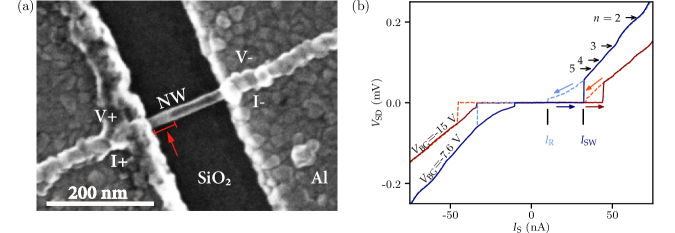
Figure 1a shows a SEM (scanning electron microscopy) image of the device with a channel length of ~ nm, designed for 4-terminal measurements. As described in detail in Ref. Ridderbos et al. (2019), Ge and/or Si inter diffuses with the Al contacts, during thermal annealing. This leaves a semiconducting island of ~ nm, which can be identified by a difference in contrast in the nanowire core on the SEM image. This has been confirmed by a TEM (transmission electron microscopy) study with an EDX (energy-dispersive x-ray) spectrum analysis on the same device (see Ref. Ridderbos et al. (2019)).
We plot the sourced current versus the measured voltage between source and drain in Fig. 1b. Sweeping forward, i. e., from to finite bias, we find that the junction switches from the superconducting state to a dissipative state at a switching current of nA at a backgate voltage while nA at V. When sweeping backwards, i. e., from finite to , the junction returns to its superconducting state at the retrapping current , resulting in hysteretic behavior. For a backgate voltage V, we find nA and a ratio , while for V, nA and a ratio . This indicates that our junction is underdamped Stewart (1968) and that , as well as the damping, depend on , mainly due to the changing number of subbands participating in transport and their position relative to the Fermi energy of the Al contacts. As described in extensive detail in Ref. Ridderbos et al. (2018), the device is tunable from full depletion (with ) to highly transparent where nA on which this work is focused.
III Junction characteristics
We will now establish whether our nanowire is ballistic or diffusive. In the ballistic case, particles traversing the junction do not scatter, except on the interfaces. In the diffusive case, particles encounter scattering sites inside the junction which leads, for example, to suppression of Du et al. (2008). For a ballistic nanowire and completely transparent interfaces, one expects the normal-state conductance to appear in multiples of the conductance quantum , and the critical current in multiples of the maximum critical current for a single subband nA Tinkham (2004). In our case, the finite interface transparency Ridderbos et al. (2018) leads to lower observed values of both the conductance and the switching current , where is suppressed by additional mechanisms such as electromagnetic coupling with the environment Jarillo-Herrero et al. (2006), premature switching and heating effects Xiang et al. (2006b); Tinkham (2004). From experiments it is therefore not trivial to conclude whether our nanowire is diffusive or ballistic and we therefore make a quantitative estimation based on calculations.
We start with estimating the elastic scattering length using Davies (1998) with the hole mobility, the effective hole mass and the Fermi velocity. We use cm2/Vs (determined at 4 K, see Conesa-Boj et al. (2017)) and for the mixed heavy and light holes Kloeffel et al. (2011); Maier et al. (2014b) with the free electron mass. To obtain the Fermi velocity we use the solutions of the Schrödinger equation for a cylindrical potential well and find the expression for the Fermi energy of the th subband with quantum number as Griffiths (1996) with the th root of the th order Bessel function and the wire radius. For the first subband this gives meV, corresponding to a Fermi velocity m/s and an estimated elastic scattering length of nm. Using a gate lever arm and the fact that the nanowire is depleted at V Ridderbos et al. (2018), we find that in the regime V we operate at 6 ( meV) to 8 ( meV) subbands, increasing to nm.
As can be seen in Fig. 1a, our nanowire channel length is ~ nm, but as discussed before, our semiconducting island is ~ nm. We are therefore far away from the diffusive limit with a corresponding coherence length of nm with . We approach the ballistic limit , with a coherence length of nm Tinkham (2004) independent of . This places the nanowire well within the ballistic limit, as is reaffirmed by the fact that the semiconducting island can be host to a single few-hole quantum dot Ridderbos et al. (2018) and that highly-tunable normal-state devices can be host to dots of length nm Brauns et al. (2016b). By increasing the Al-nanowire interface transparencies, fully ballistic junctions could therefore be realised with lengths up to a few hundred nanometer.
In Ref. Ridderbos et al. (2018) we extract an averaged eV , close to the theoretical maximum. Since our Ge-Si segment is ballistic, the Thouless energy has only meaning in terms of the time of flight through the junction fs so that mV for the sixth subband and the induced gap is therefore .
Out of the 7 devices exhibiting superconducting transport, 3 devices showed gate-tunability and Shapiro steps. There are strong indications that in the other 4 devices the Al inter-diffusion has progressed throughout the channel (see Ref. Ridderbos et al. (2019)), resulting in a completely metallic superconducting device.
IV Multiple Andreev reflections
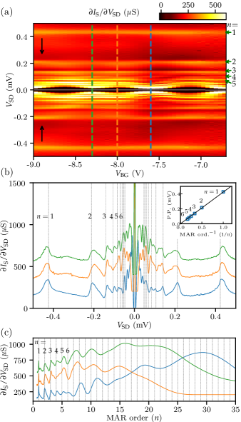
Small wiggles are visible in the versus curve for V in Fig. 1b, which are a signature of MAR. This becomes clearer in the differential conductance for a range of in Fig. 2a: the wiggles in translate to conductance peaks seen at values of corresponding to Tinkham (2004) with an integer denoting the MAR order. are indicated by the green arrows in Fig. 2a for positive bias [orders are indicated in Fig. 1(b)]. The strong conductance peak at corresponds to a supercurrent and is a direct consequence of the inversion of the and axes (see Methods), which maps onto the corresponding value of . Since a supercurrent implies for a range of , this results in a strong peak in . The height of the oscillating black regions for mV as a function of is a measure for the magnitude of (see Methods) where the oscillations correspond to varying occupation of the subbands of a weak confinement potential in the wire Ridderbos et al. (2018).
The MAR conductance peaks can be more clearly distinguished in individual linetraces in Fig. 2b and we focus on the blue trace at V. The finite width of the MAR peaks reflects the distribution of the DOS peak at and is additionally broadened by phase decoherence and inelastic processes when quasiparticles traverse the channel Nilsson et al. (2012); Tinkham (2004). We extract the peak positions (P.P.) in of the first 6 orders and plot them versus the inverse MAR order in the inset in Fig. 2b. We expect the second order MAR peak to be at the position of our superconducting gap, i. e., for , . For a more accurate estimate of we perform a linear fit through zero for the six MAR peak positions and find meV which translates to a critical temperature of our Al K Tinkham (2004). This is confirmed by an independent measurement of the of an Al stripline (not shown) and is in good agreement with the critical temperature observed in Fig. 3.
In Fig. 2b higher-order MAR peaks become increasingly hard to resolve because of the hyperbolic relation of with . In Fig. 2c, we therefore convert the x-axis from to units of , resulting in evenly spaced orders of , and plot the conductance for positive bias for the same three as in Fig. 2b. We see that for , the conductance peaks can no longer be unambiguously assigned and they span multiple . Possibly, the peak patterns for high-order MAR are a superposition of many overlapping MAR processes.
Comparing the blue curve in Fig. 2c with the orange and green curve taken at different , we observe that peak positions for lower order MAR do not perfectly reproduce, for instance, the orange curve does not show a clear peak at . We partly explain this by considering our interface transparencies which act as a weak confinement potential, resulting in highly broadened energy levels in the wire. The relative position of these levels with respect to the Fermi level changes the resonant condition for MAR, resulting in a shift of the MAR peak positions Buitelaar et al. (2003). Inspecting Fig. 2a, the high-order MAR peaks () are indeed modulated, both in intensity and position in , by the changing charge and subband population represented by the black regions at low bias ( mV).
We conclude from Fig. 2 that the resolvability of MAR up to means that quasiparticles can elastically scatter at least 6 times on the interfaces, each time traversing the nanowire channel. This requires very low inelastic scattering probabilities and a high (though finite) interface transparency Flensberg et al. (1988).
V Temperature dependence of and MAR
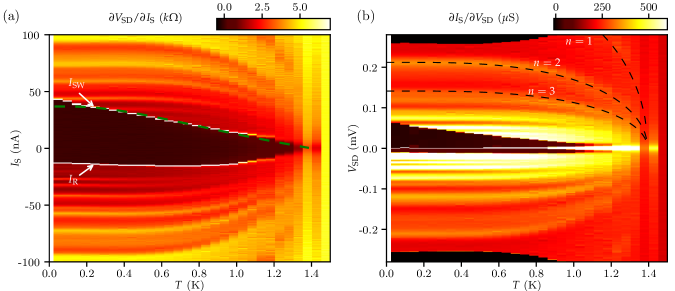
We will now investigate the temperature dependence of the switching current and the multiple Andreev reflections. In Fig. 3a we plot the differential resistance versus as a function of temperature . The black region indicates superconductivity and we can see the decrease of for increasing until disappears at K, in agreement with K calculated from . The slight increase of between - K could be due to changes in the thermal conductivity of the devices’ surroundings, leading to better thermalization at higher temperatures.
For ballistic supercurrent through a superconductor - normal metal – superconductor Josephson junction, the critical current was modeled by Galaktionov and Zaikin Galaktionov and Zaikin (2002) based on the Eilenberger equations. Note, that this model neglects the spin-orbit interaction, but arbitrary barrier transparencies can be included, and an average is provided over multiple modes. We have used this model to fit our data. As input parameters we used the critical temperature of 1.4 K, a Fermi velocity of m/s, and an electrode separation of 50 nm. These parameters completely determine the shape of the and provide a zero-temperature estimate for the average critical current of 6 nA per mode. For the experimentally measured , this would correspond to about 7 modes in the junction, consistent with our estimate of the number of modes based on the normal transport data. We furthermore obtain an average transparency of %, lower than the previously obtained transparency of % Ridderbos et al. (2018) using the BTK model Blonder et al. (1982), averaged over a large gate voltage. This difference could be explained by the fact that was only determined at a single value of and that is likely to be suppressed with respect to the actual critical current of the junction. The resulting model has been plotted in Fig. 4a, together with the experimental data.
The MAR signatures visible outside the superconducting region, scale with and therefore gradually decrease and converge to for . Figure 3b shows the same dataset as Fig. 3a converted to a voltage-biased plot (see Methods) and since for MAR order , , we have a direct measure of . We use the BCS interpolation formula Senapati et al. (2011); Kajimura and Hayakawa (2012):
| (1) |
where we replaced the pre-factor with where eV is the superconducting gap of Al at as determined in Fig. 2b. We plot this curve in Fig. 3b and find excellent agreement for the MAR peak and a good fit for . The value of corresponds to the observed K, while follows the BCS curve as a function of T, i.e., the MAR are indeed an excellent measure for the superconducting gap of the Al contacts.
VI Shapiro steps
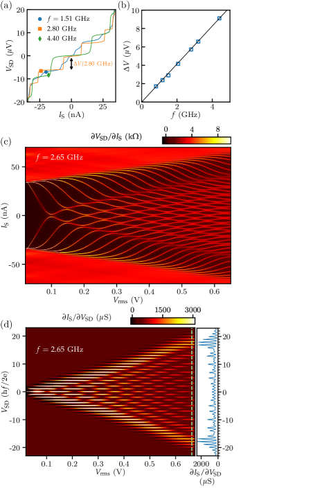
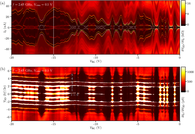
We now look at the ac Josephson effect by irradiating our junction with a antenna located ~ mm above the chip with frequencies ranging from 0.8 to 4.4 GHz. Figure 4a shows versus for three different frequencies at finite microwave amplitudes , revealing Shapiro steps in the current-voltage relation. Shapiro steps Shapiro et al. (1964) are a direct manifestation of the ac Josephson effect where phase locking occurs between the quasiparticles in the junction and the applied microwaves. Starting from the ac Josephson relation , quasiparticles can acquire a phase of per period of the applied microwave frequency with an integer denoting the Shapiro step number. We can thus write , translating to a total dc voltage Tinkham (2004) where is determined by and microwave amplitude . The extracted step height for various frequencies in Fig. 4b shows good agreement. We attribute the qualitative variation in the rounding of the steps as a function of frequency to spectral broadening of the microwaves, in turn caused by the microwave antenna properties and the coupling to the Faraday cage in which the sample resides.
We now fix the applied frequency at Ghz and plot versus and at V in Fig. 4c. When increasing , clearly visible lines of differential resistance enter the bias window, each corresponding to a stepwise increase of by constant on the plateaus enclosed by the steps. As in most experimental setups, our microwave source and antenna have a much higher impedance than our superconducting Josephson junction Tinkham (2004); Gross and Marx (2005) and it therefore acts as an ac current source. Therefore, the width of the current plateaus cannot be described by simple Bessel functions, but can only be numerically approximated Gross and Marx (2005); Russer (1972); Tinkham (2004).
To gain insight in the number of Shapiro steps and their corresponding plateau heights in Fig. 4c, we show a biased plot in units of of the same measurement data in Fig. 4d. The plateaus of constant in Fig. 4c are now visible as peaks in differential conductance . Looking at the linecut on the right we see that up to 23 steps are visible, all aligned with values of . This clear demonstration of the ac Josephson effect in Fig. 4, together with dc effects such as MAR and finite a is proof that our junction is, indeed, a well behaved Josephson junction.
VII Shapiro steps versus
Previously, was fixed at V, corresponding to a region with a high and low hysteresis, i.e. close to critical damping corresponding to a Stewart-McCumber parameter close to 1 Tinkham (2004). In Fig. 5a we show a current-sourced backgate dependence of Shapiro steps at fixed microwave frequency and power. The junction is generally hysteretic for regions with lower , observed in this figure at regions where the Shapiro steps are moving closer together on the axis. This corresponds to a higher normal state resistance which increases and results in an underdamped junction. Since measurement data were acquired in both directions while sweeping back and forth (after stepping with mV after each sweep), hysteresis appears as a white speckle pattern caused by the data acquisition alternating directions in (see for instance between and V). The observed oscillations of (and indirectly ) as a function of are again the result of the varying population of subbands.
Figure 5b shows the voltage-biased backgate dependence of the same measurement data as Fig. 5a where plateaus in current are translated to peaks in by inverting the and axis and normalising to . We identify 5 Shapiro steps which partially disappear in regions with increased when the junction is hysteretic. For this specific , steps 0, 1, and 4 disappear in the hysteretic regions, loosely corresponding to the smaller current plateau widths. Since the plateau widths vary (Bessel-like) with (see Fig. 4c), which steps are missing therefore changes as a function of (not shown here). At V, all steps are visible which is the reason this specific voltage was used in Fig. 4.
VIII Conclusion
We have realized a Josephson junction where the high interface transparency between the superconducting leads and the nanowire results in multiple Andreev reflections up to the 6th order. We additionally show up to 23 Shapiro steps, clearly demonstrating the ac Josephson effect for the first time in this system. We estimate the total contact transparency to be between 50% and 80% based on the temperature dependence and previously obtained results. We furthermore estimate the nanowire segment to be in the ballistic limit and improving the contact interfaces could therefore result in fully ballistic junctions.
Ge-Si nanowire-based Josephson junctions possess all ingredients necessary for obtaining Majorana fermions and in parallel experiments we have found very hard induced superconducting gaps Ridderbos et al. (2019). We therefore propose a follow-up experiment with a device design suitable for probing the zero-energy Majorana bound states in the nanowire Mourik et al. (2012). Additionally, other applications such as superconducting qubits and Andreev (spin) qubits, can now actively be pursued in this system.
IX Methods
IX.1 Post-processing of measurement data
All measurements in this work are performed using a 3-probe measurement. A series resistance of k was subtracted from all measurement data. In Fig. 2, Fig. 3b, Fig. 4d and Fig. 5b, the datasets are obtained using a current source driving with measurement after which a software routine is used to invert the source and measurement axis. To obtain equidistant points on the new source axis, the points are recalculated by interpolation in on a grid with predetermined stepsize. The resolution of is chosen high enough so that no features in the original measurement of are lost. In Fig. 4c and Fig. 4d a similar grid interpolation procedure was used to convert the -axis from units of dBm to V.
IX.2 MAR dataset acquisition
In the open regime MAR peaks can only be seen when the junction is in the dissipative current state and since higher-order () MAR reside close to bias, they can be obscured by the superconducting ’blind spot’ of the junction. We use the bi-stable current-voltage relation (hysteresis) of our underdamped Josephson junction in Fig. 2a, where we choose a region of with a low . In order to measure the current-voltage relation of the junction way below , the low is exploited by sweeping from finite to in both bias directions. We note that is still finite which is reflected in the small black oscillating ‘blind spot’ region around , although a much larger range of can now be probed. The visibility of MAR also depends on : a higher results in a lower voltage drop over the same , thus effectively enhancing measurement resolution of the equipotential MAR peaks. This is especially important for higher order MAR (), since its hyperbolic relation with means that the corresponding peaks become very closely spaced.
X Acknowledgements
Acknowledgements.
F.A.Z. acknowledges financial support through the Netherlands Organization for Scientific Research (NWO). E.P.A.M.B. acknowledges financial support through the EC Seventh Framework Programme (FP7-ICT) initiative under Project SiSpin No. 323841.References
- Josephson (1962) B. D. Josephson, Physics Letters 1, 251 (1962).
- Tinkham (2004) M. Tinkham, Introduction to Superconductivity Second Edition (Dover Publications, Inc., Mineola, New York, 2004).
- Shapiro (1963) S. Shapiro, Physical Review Letters 11, 80 (1963).
- Grimes and Shapiro (1968) C. C. Grimes and S. Shapiro, Physical Review 169, 397 (1968).
- Likharev (1979) K. K. Likharev, Reviews of Modern Physics 51, 101 (1979).
- Beenakker (1992) C. W. J. Beenakker, Physical Review B 46, 12841 (1992).
- Grossman (1994) E. N. Grossman, IEEE Transactions on Microwave Theory and Techniques 42, 707 (1994).
- Krive et al. (2004) I. V. Krive, S. I. Kulinich, R. I. Shekhter, and M. Jonson, Low Temperature Physics 30, 554 (2004).
- Jarillo-Herrero et al. (2006) P. Jarillo-Herrero, J. A. van Dam, and L. P. Kouwenhoven, Nature 439, 953 (2006).
- Katsaros et al. (2010) G. Katsaros, P. Spathis, M. Stoffel, F. Fournel, M. Mongillo, V. Bouchiat, F. Lefloch, A. Rastelli, O. G. Schmidt, and S. De Franceschi, Nature nanotechnology 5, 458 (2010).
- Mizuno et al. (2013) N. Mizuno, B. Nielsen, and X. Du, Nature communications 4, 2716 (2013).
- Estrada Saldaña et al. (2019) J. C. Estrada Saldaña, R. Žitko, J. P. Cleuziou, E. J. H. Lee, V. Zannier, D. Ercolani, L. Sorba, R. Aguado, and S. De Franceschi, Science Advances 5, eaav1235 (2019).
- Hendrickx et al. (2018) N. W. Hendrickx, D. P. Franke, A. Sammak, M. Kouwenhoven, D. Sabbagh, L. Yeoh, R. Li, M. L. V. Tagliaferri, M. Virgilio, G. Capellini, G. Scappucci, and M. Veldhorst, Nature Communications 9, 2835 (2018).
- Kim et al. (2016) H.-S. Kim, B.-K. Kim, Y. Yang, X. Peng, S.-G. Lee, D. Yu, and Y.-J. Doh, Applied Physics Express 9, 023102 (2016).
- Cleuziou et al. (2006) J. Cleuziou, W. Wernsdorfer, V. Bouchiat, T. Ondarçuhu, and M. Monthioux, Nature Nanotechnology 1, 53 (2006).
- Vigneau et al. (2019) F. Vigneau, R. Mizokuchi, D. C. Zanuz, X. Huang, S. Tan, R. Maurand, S. Frolov, A. Sammak, G. Scappucci, F. Lefloch, and S. De Franceschi, Nano Letters 19, 1023 (2019).
- van Dam et al. (2006) J. A. van Dam, Y. V. Nazarov, E. P. A. M. Bakkers, S. De Franceschi, and L. P. Kouwenhoven, Nature 442, 667 (2006).
- Jørgensen et al. (2007) H. I. Jørgensen, T. Novotný, K. Grove-Rasmussen, K. Flensberg, and P. E. Lindelof, Nano Letters 7, 2441 (2007).
- Delagrange et al. (2018) R. Delagrange, R. Weil, A. Kasumov, M. Ferrier, H. Bouchiat, and R. Deblock, Physica B: Condensed Matter 536, 211 (2018).
- Hofstetter et al. (2009) L. Hofstetter, S. Csonka, J. Nygard, and C. Schonenberger, Nature 461, 960 (2009).
- Tan et al. (2015) Z. B. Tan, D. Cox, T. Nieminen, P. Lähteenmäki, D. Golubev, G. B. Lesovik, and P. J. Hakonen, Physical Review Letters 114, 096602 (2015).
- de Lange et al. (2015) G. de Lange, B. van Heck, A. Bruno, D. J. van Woerkom, A. Geresdi, S. R. Plissard, E. P. A. M. Bakkers, A. R. Akhmerov, and L. DiCarlo, Physical Review Letters 115, 127002 (2015).
- Larsen et al. (2015) T. W. Larsen, K. D. Petersson, F. Kuemmeth, T. S. Jespersen, P. Krogstrup, J. Nygård, and C. M. Marcus, Physical Review Letters 115, 127001 (2015).
- Mergenthaler et al. (2019) M. Mergenthaler, A. Nersisyan, A. Patterson, M. Esposito, A. Baumgartner, C. Schönenberger, G. A. D. Briggs, E. A. Laird, and P. J. Leek, 1 (2019).
- Kroll et al. (2018) J. G. Kroll, W. Uilhoorn, K. L. van der Enden, D. de Jong, K. Watanabe, T. Taniguchi, S. Goswami, M. C. Cassidy, and L. P. Kouwenhoven, Nature Communications 9, 4615 (2018).
- Casparis et al. (2018) L. Casparis, M. R. Connolly, M. Kjaergaard, N. J. Pearson, A. Kringhøj, T. W. Larsen, F. Kuemmeth, T. Wang, C. Thomas, S. Gronin, G. C. Gardner, M. J. Manfra, C. M. Marcus, and K. D. Petersson, Nature Nanotechnology 13, 915 (2018).
- Kitaev (2001) A. Y. Kitaev, Physics-Uspekhi 44, 131 (2001).
- Mourik et al. (2012) V. Mourik, K. Zuo, S. M. Frolov, S. R. Plissard, E. P. A. M. Bakkers, and L. P. Kouwenhoven, Science 336, 1003 (2012).
- Deng et al. (2016) M. T. Deng, S. Vaitiekėnas, E. B. Hansen, J. Danon, M. Leijnse, K. Flensberg, J. Nygård, P. Krogstrup, and C. M. Marcus, Science 354, 1557 (2016).
- Aguado (2017) R. Aguado, Rivista del Nuovo Cimento 40, 523 (2017).
- Lutchyn et al. (2018) R. M. Lutchyn, E. P. A. M. Bakkers, L. P. Kouwenhoven, P. Krogstrup, C. M. Marcus, and Y. Oreg, Nature Reviews Materials 3, 52 (2018).
- Gül et al. (2018) Ö. Gül, H. Zhang, J. D. S. Bommer, M. W. A. de Moor, D. Car, S. R. Plissard, E. P. A. M. Bakkers, A. Geresdi, K. Watanabe, T. Taniguchi, and L. P. Kouwenhoven, Nature Nanotechnology 13, 192 (2018).
- Hu et al. (2007) Y. Hu, H. O. H. Churchill, D. J. Reilly, J. Xiang, C. M. Lieber, and C. M. Marcus, Nature Nanotechnology 2, 622 (2007).
- Hu et al. (2012) Y. Hu, F. Kuemmeth, C. M. Lieber, and C. M. Marcus, Nature nanotechnology 7, 47 (2012).
- Higginbotham et al. (2014a) A. P. Higginbotham, F. Kuemmeth, M. P. Hanson, A. C. Gossard, and C. M. Marcus, Physical Review Letters 112, 026801 (2014a).
- Higginbotham et al. (2014b) A. P. Higginbotham, T. W. Larsen, J. Yao, H. Yan, C. M. Lieber, C. M. Marcus, and F. Kuemmeth, Nano Letters 14, 3582 (2014b).
- Brauns et al. (2016a) M. Brauns, J. Ridderbos, A. Li, E. P. A. M. Bakkers, and F. A. Zwanenburg, Physical Review B 93, 121408(R) (2016a).
- Brauns et al. (2016b) M. Brauns, J. Ridderbos, A. Li, W. G. van der Wiel, E. P. A. M. Bakkers, and F. A. Zwanenburg, Applied Physics Letters 109, 143113 (2016b).
- Brauns et al. (2016c) M. Brauns, J. Ridderbos, A. Li, E. P. A. M. Bakkers, W. G. van der Wiel, and F. A. Zwanenburg, Physical Review B 94, 041411(R) (2016c).
- Zarassi et al. (2017) A. Zarassi, Z. Su, J. Danon, J. Schwenderling, M. Hocevar, B. M. Nguyen, J. Yoo, S. A. Dayeh, and S. M. Frolov, Physical Review B 95, 155416 (2017).
- Froning et al. (2018) F. N. M. Froning, M. K. Rehmann, J. Ridderbos, M. Brauns, F. A. Zwanenburg, A. Li, E. P. A. M. Bakkers, D. M. Zumbühl, and F. R. Braakman, Applied Physics Letters 113, 073102 (2018).
- Xiang et al. (2006a) J. Xiang, W. Lu, Y. Hu, Y. Wu, H. Yan, and C. M. Lieber, Nature 441, 489 (2006a).
- Su et al. (2016) Z. Su, A. Zarassi, B.-M. Nguyen, J. Yoo, S. A. Dayeh, and S. M. Frolov, arXiv:1610.03010 (2016).
- Ridderbos et al. (2018) J. Ridderbos, M. Brauns, J. Shen, F. K. de Vries, A. Li, E. P. A. M. Bakkers, A. Brinkman, and F. A. Zwanenburg, Advanced Materials 30, 1802257 (2018).
- de Vries et al. (2018) F. K. de Vries, J. Shen, R. J. Skolasinski, M. P. Nowak, D. Varjas, L. Wang, M. Wimmer, J. Ridderbos, F. A. Zwanenburg, A. Li, S. Koelling, M. A. Verheijen, E. P. A. M. Bakkers, and L. P. Kouwenhoven, Nano Letters 18, 6483 (2018).
- Maier et al. (2014a) F. Maier, J. Klinovaja, and D. Loss, Physical Review B 90, 195421 (2014a).
- Chtchelkatchev and Nazarov (2003) N. M. Chtchelkatchev and Y. V. Nazarov, Physical Review Letters 90, 226806 (2003).
- Zazunov et al. (2003) A. Zazunov, V. S. Shumeiko, E. N. Bratus’, J. Lantz, and G. Wendin, Physical Review Letters 90, 087003 (2003).
- Padurariu and Nazarov (2010) C. Padurariu and Y. V. Nazarov, Physical Review B 81, 144519 (2010).
- Janvier et al. (2015) C. Janvier, L. Tosi, L. Bretheau, Ç. Ö. Girit, M. Stern, P. Bertet, P. Joyez, D. Vion, D. Esteve, M. F. Goffman, H. Pothier, and C. Urbina, Science 349, 1199 (2015).
- van Woerkom et al. (2017) D. J. van Woerkom, A. Proutski, B. van Heck, D. Bouman, J. I. Väyrynen, L. I. Glazman, P. Krogstrup, J. Nygård, L. P. Kouwenhoven, and A. Geresdi, Nature Physics 13, 876 (2017).
- Hays et al. (2018) M. Hays, G. de Lange, K. Serniak, D. J. van Woerkom, D. Bouman, P. Krogstrup, J. Nygård, A. Geresdi, and M. H. Devoret, Physical Review Letters 121, 047001 (2018).
- Tosi et al. (2019) L. Tosi, C. Metzger, M. F. Goffman, C. Urbina, H. Pothier, S. Park, A. L. Yeyati, J. Nygård, and P. Krogstrup, Physical Review X 9, 011010 (2019).
- Kloeffel et al. (2011) C. Kloeffel, M. Trif, and D. Loss, Physical Review B 84, 195314 (2011).
- Higginbotham et al. (2014c) A. P. Higginbotham, F. Kuemmeth, T. W. Larsen, M. Fitzpatrick, J. Yao, H. Yan, C. M. Lieber, and C. M. Marcus, Physical Review Letters 112, 216806 (2014c).
- Itoh et al. (2003) K. M. Itoh, J. Kato, M. Uemura, A. K. Kaliteevskii, O. N. Godisov, G. G. Devyatych, A. D. Bulanov, A. V. Gusev, I. D. Kovalev, P. G. Sennikov, H.-J. Pohl, N. V. Abrosimov, and H. Riemann, Japanese Journal of Applied Physics 42, 6248 (2003).
- Kuhlmann et al. (1994) M. Kuhlmann, U. Zimmermann, D. Dikin, S. Abens, K. Keck, and V. M. Dmitriev, Zeitschrift für Physik B Condensed Matter 96, 13 (1994).
- Flensberg and Hansen (1989) K. Flensberg and J. B. Hansen, Physical Review B 40, 8693 (1989).
- Ridderbos et al. (2019) J. Ridderbos, M. Brauns, J. Shen, F. K. de Vries, A. Li, S. Kölling, M. A. Verheijen, A. Brinkman, W. G. van der Wiel, E. P. A. M. Bakkers, and F. A. Zwanenburg, arXiv:1907.05510 (2019).
- Stewart (1968) W. C. Stewart, Applied Physics Letters 12, 277 (1968).
- Du et al. (2008) X. Du, I. Skachko, and E. Y. Andrei, Physical Review B 77, 184507 (2008).
- Xiang et al. (2006b) J. Xiang, A. Vidan, M. Tinkham, R. M. Westervelt, and C. M. Lieber, Nature Nanotechnology 1, 208 (2006b).
- Davies (1998) J. H. Davies, The physics of low-dimensional semiconductors (Cambridge University, New York, 1998).
- Conesa-Boj et al. (2017) S. Conesa-Boj, A. Li, S. Koelling, M. Brauns, J. Ridderbos, T. T. Nguyen, M. A. Verheijen, P. M. Koenraad, F. A. Zwanenburg, and E. P. A. M. Bakkers, Nano Letters 17, 2259 (2017).
- Maier et al. (2014b) F. Maier, T. Meng, and D. Loss, Physical Review B 90, 155437 (2014b).
- Griffiths (1996) D. J. Griffiths, Introduction to Quantum Mechanics (Cambridge University Press, 1996).
- Nilsson et al. (2012) H. A. Nilsson, P. Samuelsson, P. Caroff, and H. Q. Xu, Nano Letters 12, 228 (2012).
- Buitelaar et al. (2003) M. R. Buitelaar, W. Belzig, T. Nussbaumer, B. Babić, C. Bruder, and C. Schönenberger, Physical Review Letters 91, 057005 (2003).
- Flensberg et al. (1988) K. Flensberg, J. B. Hansen, and M. Octavio, Physical Review B 38, 8707 (1988).
- Galaktionov and Zaikin (2002) A. V. Galaktionov and A. D. Zaikin, Physical Review B 65, 184507 (2002).
- Blonder et al. (1982) G. E. Blonder, M. Tinkham, and T. M. Klapwijk, Physical Review B 25, 4515 (1982).
- Senapati et al. (2011) K. Senapati, M. G. Blamire, and Z. H. Barber, Nature Materials 10, 849 (2011).
- Kajimura and Hayakawa (2012) K. Kajimura and H. Hayakawa, Advances in Superconductivity III: Proceedings of the 3rd International Symposium on Superconductivity (ISS ’90), November 6–9, 1990, Sendai (Springer Japan, 2012) p. 1320.
- Shapiro et al. (1964) S. Shapiro, A. R. Janus, and S. Holly, Reviews of Modern Physics 36, 223 (1964).
- Gross and Marx (2005) R. Gross and A. Marx, Applied superconductivity,, Vol. 1 (2005) p. 480.
- Russer (1972) P. Russer, Journal of Applied Physics 43, 2008 (1972).