A bi-directional Address-Event transceiver block for low-latency inter-chip communication in neuromorphic systems
Abstract
Neuromorphic systems typically use the Address-Event Representation (AER) to transmit signals among nodes, cores, and chips. Communication of Address-Events between neuromorphic cores/chips typically requires two parallel digital signal buses for Input/Output (I/O) operations. This requirement can become very expensive for large-scale systems in terms of both dedicated I/O pins and power consumption. In this paper we present a compact fully asynchronous event-driven transmitter/receiver block that is both power efficient and I/O efficient. This block implements high-throughput low-latency bi-directional communication through a parallel AER bus. We show that by placing the proposed AE transceiver block in two separate chips and linking them by a single AER bus, we can drive the communication and switch the transmission direction of the shared bus on a single event basis, from either side with low-latency. We present experimental results that validate the circuits proposed and demonstrate reliable bi-directional event transmission with high-throughput. The proposed AE block, integrated in a neuromorphic chip fabricated using a 28 nm FDSOI process, occupies a silicon die area of 140 m 70 m. The experimental measurements show that the event-driven AE block combined with standard digital I/Os has a direction switch latency of 5 ns and can achieve a worst-case bi-directional event transmission throughput of 28.6 MEvents/second while consuming 11 pJ per event (26-bit) delivery.
I Introduction
The AER has been widely used in brain-inspired neuromorphic systems as a communication protocol for transmitting and receiving spikes encoded as AEs among spiking silicon neurons and synapses. For example dynamic vision sensors [1] and silicon cochleas [2] use the AER to transmit their sensory processing outputs to AERs neuromorphic processors and transceivers [Park_etal14, 6, Furber_etal14, 3, 4]. As these types of neuromorphic VLSI systems typically require AEs to be transmitted with high throughput and low latency, the strategy employed to implement the communication protocol makes use of asynchronous bit-parallel AER channels. This strategy however is not scalable, as the width of the parallel bus and the power required to transmit these parallel events scales with the size of the network. In addition, the pin count and power requirements become even larger if one desires to build modular systems with north/south, east/west I/O links necessary to tile multiple cores or chips in 2D arrays [6, 4]. Instead of simple pure parallel AER protocol, some approaches use a “word-serial” protocol to transmit multiple row addresses for every column address serviced (or vice-versa) to reduce pin numbers [Boahen04, 7]. Furthermore, bit-serial Low Voltage Differential Signaling (LVDS) AER has been proposed as a potential solution to transmit events in a fully bit-serial format to further reduce pin numbers [8]. However, these approaches lead to significant increment in latency and overhead for the complexity of the circuit implementation. Moreover, the design proposed in [8] needs additional clock generation and synchronization circuits which is expensive for fully asynchronous neuromorphic system.
In this paper, we present a compact fully-asynchronous event-driven AE transceiver block which can be easily combined with standard digital I/Os to realize bi-directional inter-chip AE communication through a single parallel AER bus with high-throughput and low-latency. In the next Section, we introduce architecture of the proposed AE transceiver block. In Section III, we describe the circuits that implement the proposed bi-directional AER block. In Section IV we present experimental results obtained from the measurements of a test chip fabricated in 28 nm FDSOI process. We present concluding remarks and discussion in Section V.
II Architecture
| SW_reqL (SW_ackR) | SW_ackL (SW_reqR) | Left Mode | Right Mode |
|---|---|---|---|
| 0 | 1 | TX | RX |
| 1 | TX | RX | |
| 1 | TXRX | RXTX | |
| 1 | RX | TX | |
| 1 | RXTX | TXRX |
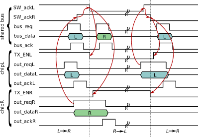
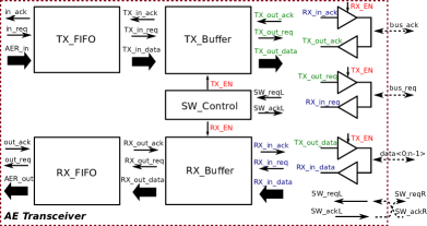
Figure 1 shows the architecture of the proposed AE transceiver block. Bi-directional chip communication can be implemented by connecting two AE transceiver blocks directly with a single shared bit-parallel AER bus. As is shown in Fig. 1, and from two linked AE blocks are swapped and connected to announce state of each other. The SW_Control block in each AE transceiver block then checks the states of two connected chip which are indicated by and , and generates control signals to allow TX_Buffer to push events on the shared AER bus or allow RX_Buffer to take events from the bus. Each AE block use to identify its own states (i.e., logic “1” if this AE block need to switch to transmitter mode “TX” for transmitting events, and logic “0” if currently this AE block has no event to transmit and can be switched to receiver mode “RX”), and use to get states of it’s linked AE block. SW_Control block on both sides will generate control signals and to switch on/off TX_Buffer and RX_Buffer and alternatively map terminals of TX_Buffer or RX_Buffer to the shared bus for a mode switching. Table I shows how modes are switched in different cases, with representing logic “0” to “1” and representing logic “1” to “0”.
Moreover, conditions need to be met for a safe mode switching. An AE transceiver block will only request a mode switching RXTX by asserting its SW_ack when: 1) The block is currently in a “RX” mode; 2)The block has received at least one event in “RX” mode (except that this block is initially reset to “RX” mode for a chip-level global reset); And 3) one or more events need to be transmitted. An AE transceiver block will only acknowledge a mode switching request from its lined AE block by de-asserting its SW_ack when: 1) The block is currently in a “TX” mode, and 2) it received a mode switching request.
Figure 2 shows an example how bi-directional transmission is implemented with proposed AE transceiver block following 4-phase handshaking. Assume that two AE transceiver blocks are linked by a signal AER bus, and initially we set of left block to logic “1” and of right block to logic “0”. So that initially the left AE block is in “TX” mode and the right AE block is in “RX” mode, to allow event transmission from left to right. Once there is an event need to be transmitted on right side, will be assert to “1” to request a mode switching. After requested by , as soon as there is no more event need to be transmitted by the left AE block, will be deassert to “0” to acknowledge the mode switching request. Correspondingly, in both blocks will be flipped to complete the mode switching.
Bi-directional tri-state buffers as shown in Fig. 1 are then switched by for mapping signals of TX/RX_Buffer blocks to shared AER bus. We should notice that the tri-state buffers can be directly replaced with standard digital I/O with as a configure signal for Input/Output switching. Input and output FIFOs are added to increase throughput of proposed AE transceiver block.
III Circuits Implementation
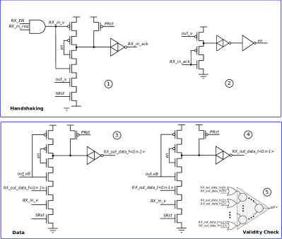
The proposed AE transceiver block is implemented following 4-phase handshaking protocol based on Pre-Charge Half-Buffer (PCHB). Figure 3 shows circuit implementation of SW_Control block for controlling mode switching. RX_Probe is employed to probe whether the belonging AE block has received at least one event as a receiver ( = “1”) in “RX” mode ( = “1”). TX_Probe is used to probe whether currently the belonging AE transceiver block has no event to be transmitted ( = “0”) as a transmitter in “TX” mode ( = “1”) when its linked AE transceiver block requests to switch the mode (). Switch Controller sub-block requests a mode switching RXTX (by asserting to “1”) when a coming event needs to be transmitted ( = “1”) if its belonging AE transceiver block is currently in “RX” mode ( = “1”) and it has successfully received at least one event ( = “1”) in “RX” mode. Three NFETs in Switch Controller sub-block gated by , and implement these guards. Switch Controller block also acknowledges a mode switching request from its linked AE transceiver block for a mode switching TXRX ( = “1”) if currently no event needs to be transmitted ( = “0”). Two p-FETs in Switch Controller sub-block gated by and implement these guards.
As described in previous section, If the AE transceiver block requested a mode switching RXTX and its linked AE block has acknowledged this request ( = “1” = “0”) , this AE block will be switched to “TX” mode ( = “1”). Otherwise, if this AE transmission block has acknowledged a mode switching TXRX requested by its linked AE block ( = “1” = “0”), this AE block will be switched to “RX” mode (= “1”). In these figures, signal ends with “B” represent reversed signal. Logic gates gated by , are global reset signals used to reset TX and RX Probes to an initial state, for example, is reset to “0” for “TX” mode or “1” for “RX” mode.
Figure 4 shows transistor level circuit implementation of TX_Buffer based on PCHB, following 4-phase bundled-data handshaking protocol. The process stage includes Handshaking and Data function blocks. Block ① guarantees that the process stage only deal with coming events while the linked AE transceiver block is free ( = “0”). Block ② checks whether the processing progress is completed to generate handshaking signal for previous process stage. Block ③ generates internal enable signal to enable functional processing. Matched delay element ④ is added to provide the worst case latency of buffer operation from valid input event data to output event. Block ⑤ implements an event buffer function.
RX_Buffer following 4-phase rail-rail handshaking protocol based on PCHB is shown in Fig. 5. Block ① checks whether the processing progress is completed and generates acknowledge signal to acknowledge previous process stage for a valid input and completed valid output. Block ② generates internal enable signal to enable functional processing. Dual-rail protocol (block ③ and ④ ) is utilized in this RX_Buffer and following RX_FIFO stage for Quasi-Delay Insensitive (QDI) processes. Validity check block ⑤ is employed to indicate output data from this process stage is valid.


IV Experimental Results
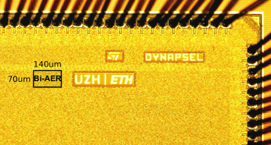
The proposed AE transceiver block is implemented and placed at all chip boarders of a neuromorphic chip in 28 nm FDSOI process [9] for implementing 2D chip-array bi-directional 26-bit AER communication. Standard digital I/Os with driven ability of 2 mA are adopted and internally configured by and for switching event transmission direction. As is shown in Fig. 6, each AE block occupies a silicon area of 140 m 70 m. By easily utilizing proposed AE blocks, we saved 100 I/Os which is a significant reducing for a prototype chip with totally 180 I/Os.
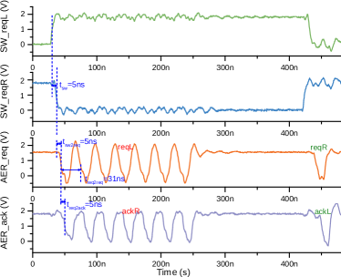
In order to judge the performance, we first measured single direction events transmission performance by continuously sending address events from single direction. As is shown in Fig. 7, AE transceivers from two linked chips are first reset to transmission direction from right to left. For continuously events communing from left, AE blocks first need to switch transmission direction with a switching latency of around 5 ns. Latency from a successfully mode switching to asserting the first request is around 5 ns. For continuously single direction events transmission, latency between two requests is around 31 ns, with a throughput of 32.3 MEvents/second.
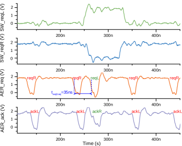
For bi-directional transmission, we transmitted events from both directions of two linked AE blocks. As is shown in Fig. 8, request latency of two events from two directions is around 35 ns, with an achieved worst case bi-directional throughput of 28.6 MEvents/second. Energy for delivering one 26-bit event is 11 pJ at 1 V power supply, excluding power consumption from digital IOs.
A summary of the key figures of the proposed AE transceiver block is shown in Table II.
| Process Technology | 28 nm FDSOI |
|---|---|
| Silicon Area | 140 m 70 m |
| Throughput (with IO) | 32.3 MEvents/s / 28.6 MEvents/s (bi-directional) |
| Latency | 5 ns |
| Energy per Event (26-bit) | 11 pJ@1 V |
V Conclusions
We presented a compact low-power event-driven bi-directional AE transceiver block for high-throughput and low-latency bi-directional inter-chip communication. The proposed fully asynchronous AE block is compatible with standard digital I/Os for easily implementing bi-directional inter-chip communication while saving half I/Os, comparing with normal bit-parallel AER protocol. Furthermore, it is possible to combine proposed scheme with "sub-words" to further reduce I/O numbers and power consumption. We designed and fabricated the proposed AE transmission block in 28 nm FDSOI process with an area of 140 m 70 m. Combined with standard digital I/Os, we implemented 2D spiking neural network bi-directional chip-array communication. Chip measurements show that the proposed AE transceiver block can achieve a worst case bi-directional event throughput of 28.6 MEvents/s with energy per event 11 pJ at 1 V supply voltage. The latency for switching transmission direction between two AE transmission blocks is around 5 ns.
Acknowledgment
This work is supported by the EU ERC grant “NeuroP” (257219) and by the EU ICT grant “NeuRAM3” (687299).
References
- [1] T. Delbruck, B. Linares-Barranco, E. Culurciello, and C. Posch, “Activity-driven, event-based vision sensors,” in International Symposium on Circuits and Systems, (ISCAS), 2010. Paris, France: IEEE, 2010, pp. 2426–2429.
- [2] S.-C. Liu, A. van Schaik, B. Minch, T. Delbruck et al., “Asynchronous binaural spatial audition sensor with 2x64 4 channel output,” Biomedical Circuits and Systems, IEEE Transactions on, vol. 8, no. 4, pp. 453–464, 2014.
- [3] N. Qiao, H. Mostafa, F. Corradi, M. Osswald, F. Stefanini, D. Sumislawska, and G. Indiveri, “A re-configurable on-line learning spiking neuromorphic processor comprising 256 neurons and 128k synapses,” Frontiers in Neuroscience, vol. 9, no. 141, 2015. [Online]. Available: http://www.frontiersin.org/neuromorphic_engineering/10.3389/fnins.2015.00141/abstract
- [4] S. Moradi, N. Qiao, F. Stefanini, and G. Indiveri, “A scalable multi-core architecture with heterogeneous memory structures for dynamic neuromorphic asynchronous processors (dynaps),” arXiv preprint arXiv:1708.04198, 2017.
- [5] G. Indiveri, F. Corradi, and N. Qiao, “Neuromorphic architectures for spiking deep neural networks,” in Electron Devices Meeting (IEDM), 2015 IEEE International. IEEE, Dec. 2015, pp. 4.2.1–4.2.14. [Online]. Available: http://ncs.ethz.ch/pubs/pdf/Indiveri_etal15.pdf
- [6] P. A. Merolla, J. V. Arthur, R. Alvarez-Icaza, A. S. Cassidy, J. Sawada, F. Akopyan, B. L. Jackson, N. Imam, C. Guo, Y. Nakamura, B. Brezzo, I. Vo, S. K. Esser, R. Appuswamy, B. Taba, A. Amir, M. D. Flickner, W. P. Risk, R. Manohar, and D. S. Modha, “A million spiking-neuron integrated circuit with a scalable communication network and interface,” Science, vol. 345, no. 6197, pp. 668–673, Aug. 2014. [Online]. Available: http://www.sciencemag.org/content/345/6197/668
- [7] C. Brandli, R. Berner, M. Yang, S.-C. Liu, and T. Delbruck, “A 240180 130 dB 3 s latency global shutter spatiotemporal vision sensor,” IEEE Journal of Solid-State Circuits, vol. 49, no. 10, pp. 2333–2341, 2014.
- [8] C. Zamarreño-Ramos, R. Kulkarni, J. Silva-Martínez, T. Serrano-Gotarredona, and B. Linares-Barranco, “A 1.5 ns off/on switching-time voltage-mode lvds driver/receiver pair for asynchronous aer bit-serial chip grid links with up to 40 times event-rate dependent power savings,” IEEE transactions on biomedical circuits and systems, vol. 7, no. 5, pp. 722–731, 2013.
- [9] N. Qiao and G. Indiveri, “Scaling mixed-signal neuromorphic processors to 28 nm fd-soi technologies,” in Biomedical Circuits and Systems Conference (BioCAS), 2016 IEEE. IEEE, 2016, pp. 552–555.