Scaling mixed-signal neuromorphic processors to 28 nm FD-SOI technologies
Abstract
As processes continue to scale aggressively, the design of deep sub-micron, mixed-signal design is becoming more and more challenging. In this paper we present an analysis of scaling multi-core mixed-signal neuromorphic processors to advanced 28 nm FD-SOI nodes. We address analog design issues which arise from the use of advanced process, including the problem of large leakage currents and device mismatch, and asynchronous digital design issues. We present the outcome of Monte Carlo Analysis and circuit simulations of neuromorphic subthreshold analog/digital neuron circuits which reproduce biologically plausible responses. We describe the AER used to implement PCHB based asynchronous QDI routing processes in multi-core neuromorphic architectures and validate their operation via circuit simulation results. Finally we describe the implementation of custom 28 nm CAM based memory resources utilized in these multi-core neuromorphic processor and discuss the possibility of increasing density by using advanced RRAM devices integrated in the 28 nm Fully-Depleted Silicon on Insulator (FD-SOI) process.
I Introduction
Neural networks and deep learning models have recently become the state of the art architectures for a wide range of applications that include data mining, signal processing, and pattern recognition [1]. However, most of these architectures are modeled as algorithms executed on power-hungry central processing units (CPUs) or graphical processing units (GPUs), often integrated in large server farms of classical von Neumann computing systems. Neuromorphic processors represent a promising alternative brain-inspired technology that, thanks to their massively parallel computational substrate, are ideally suited for implementing such algorithms [2, 3, 4, 5, 6]. These hardware devices promise to reduce power consumption by several orders of magnitude and have the potential to solve the von Neumann memory bottleneck problem thanks to their co-localized memory and computing features [7].
While neuromorphic processors made using purely digital circuits are already being implemented in advanced scaled processes [2, 4], devices designed using mixed analog and digital circuits have been implemented typically using older, less aggressive CMOS processes, such as 180 nm [6, 3].
In this paper we show how subthreshold analog designs can be scaled effectively down to 28 nm processes using FD-SOI technology. We use as a reference design the analog silicon neuron described in [6] and analyze its performance and characteristics in the 28 nm FD-SOI process, addressing issues related to channel and gate leakage currents, as well as device mismatch. Moreover, we describe the set of asynchronous digital circuits that can be used to interconnect multiple instances of these neurons among each others in single-chip multi-core architectures, and provide estimates for their size, bandwidth and power consumption in these scaled processes.
II Key sub-circuits in 28 nm FD-SOI processes
The transistors operated in the subthreshold regime used in mixed signal analog/digital neuromorphic architectures implemented with 180 nm or larger feature size CMOS processes typically use currents ranging from tens of nA to currents as low as a few pA [8]. Minimum-size transistors in advanced processes have considerably larger leakage currents. To maintain these levels of currents, we performed circuit simulations of single transistors and determined their proper geometrical size. Based on these results, we optimized the design of the analog silicon neuron circuit shown in Fig. 2, and performed Monte Carlo simulations to validate its performance in the 28 nm FD-SOI process.
To build multi-neuron/multi-core architectures using these analog neuron circuits, we make use of asynchronous Address-Event Representation (AER) digital circuits. These circuits assign a tag to the neuron that spikes and route its address to one or more destinations. Routing tables and tag memories are distributed within and across the neuron arrays, and can be programmed using the same AER communication protocol. Different neural network configurations, such as convolutional networks, deep multi-layer networks, or recurrent reservoir networks, can be deployed, depending on how these memory structures are programmed. To evaluate performance of typical asynchronous AER circuits in the 28 nm FD-SOI process considered, we designed and simulated a 10-bit pipeline buffer process stage. The type of digital memories we considered for storing the tags used to route spikes from source neurons to destination synapses are Content Addressable Memorys. As these are integral part of the synapse modules, and as neuromorphic processors typically consist of large arrays of synaptic elements, these memory circuits are the ones that would occupy the main area of the chip. We discuss possible scaling strategies for implementing CAMs in order to minimize the area of the die size, in the 28 nm FD-SOI process, given a specific network size.
II-A The analog subthreshold Integrate&Fire neuron
To develop mixed signal analog/digital neuromorphic processors that can be used in closed-loop application scenarios (e.g. ranging from self-driving cars to biomedical micro-devices measuring metabolites in the blood stream and deciding on what actions to take), it is necessary to endow them with computational elements that have time constants that are well-matched to the signals they are meant to process [5]. For natural signals (speech, gestures, etc.) these signals typically involve time constants of the order of milliseconds. It has been shown [6] that to achieve these time constants with the silicon neuron of Fig. 2, given a membrane capacitance of 1 pF, it is necessary to use currents of the order of a few pA.
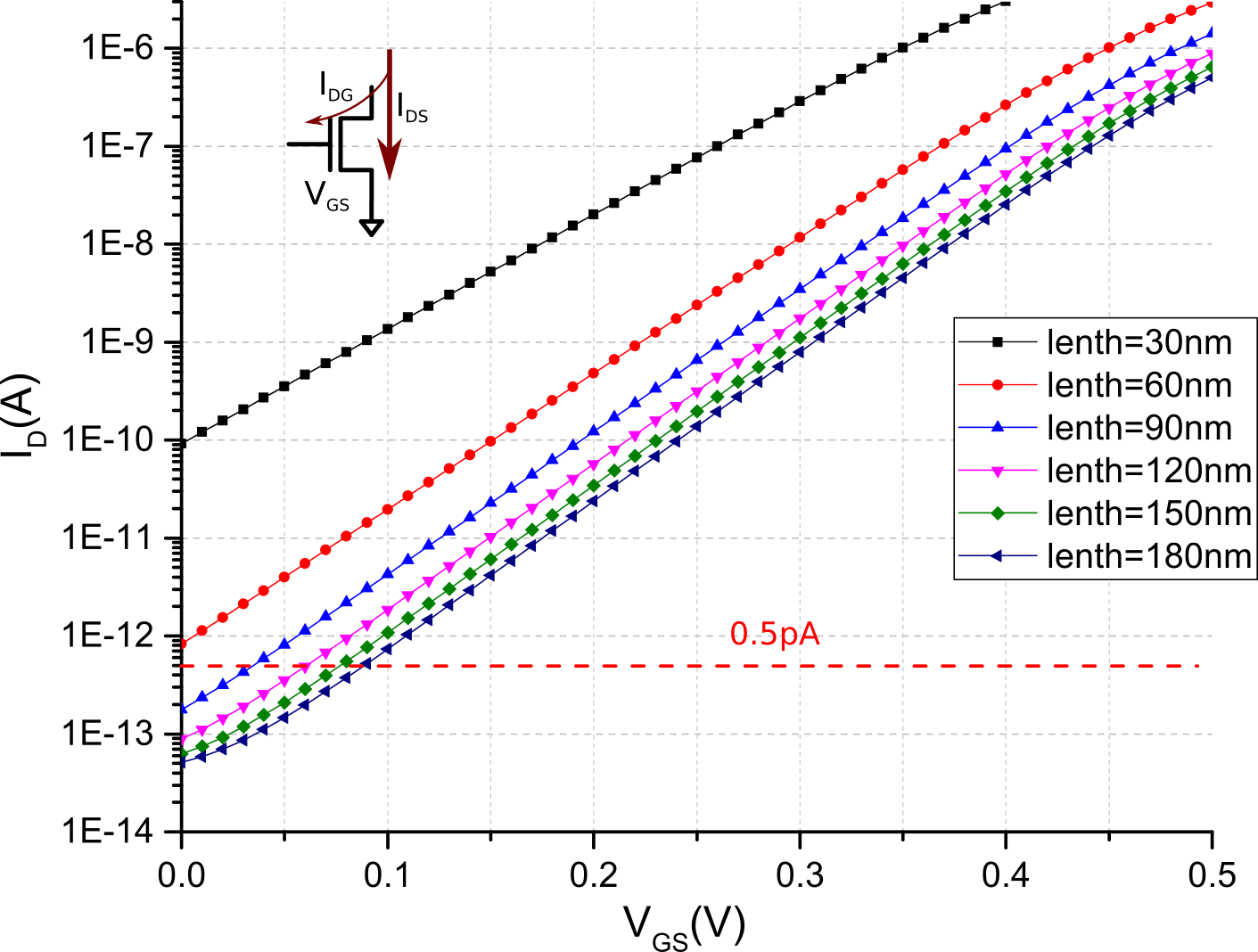
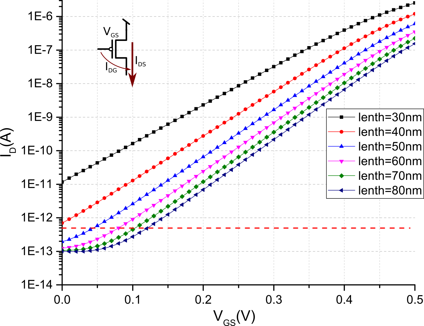
Figure 1 shows simulated current of PMOS/NMOS versus in subthreshold region for different channel lengths, with a fixed and .
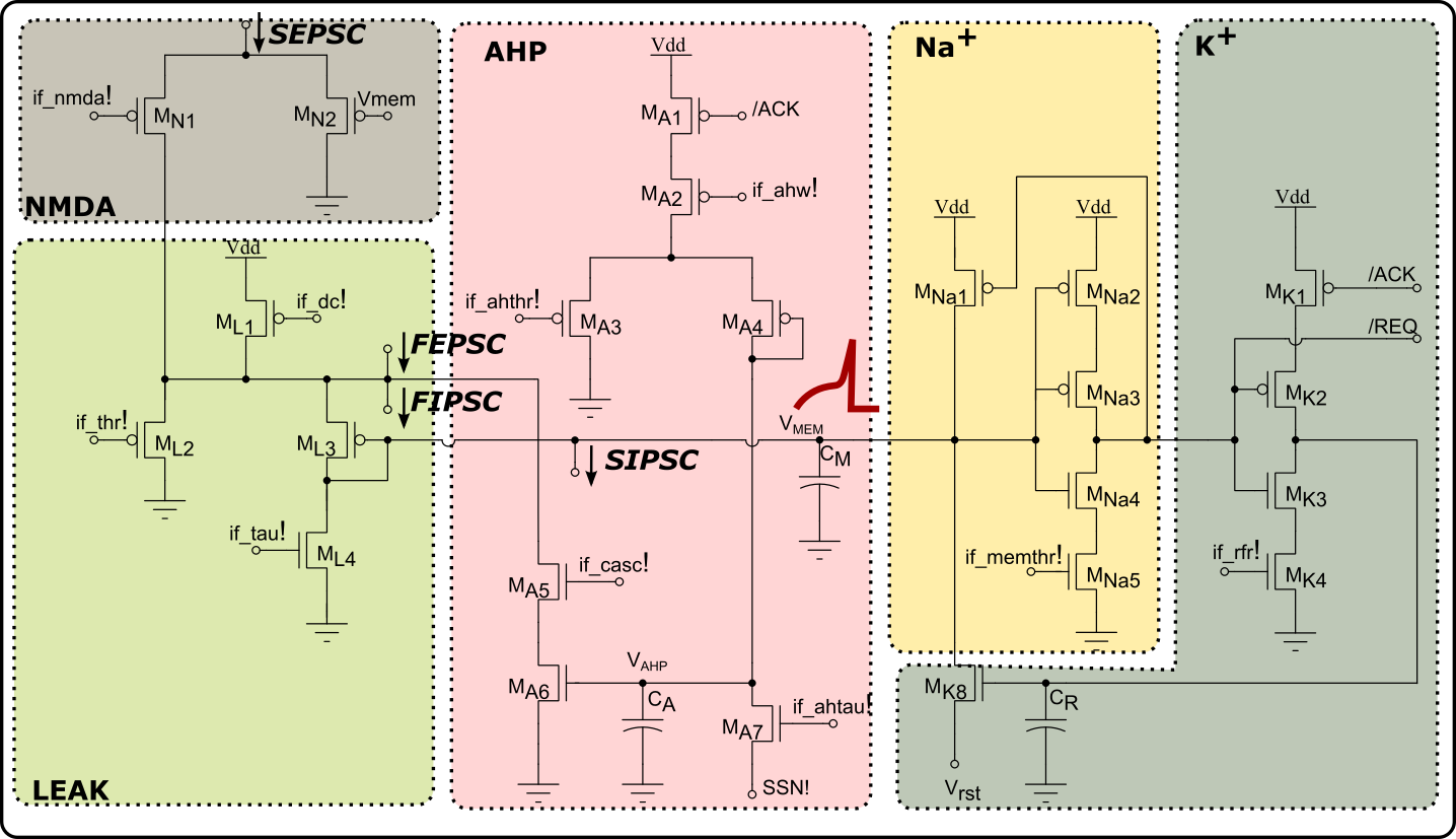
A simplified subthreshold analog neuron circuit compatible with the 28 nm FD-SOI process is shown in Fig. 2. Input currents are injected into the neuron membrane capacitance , in parallel with a programmable constant DC current. The NMDA block models the voltage-gating mechanisms of NMDA synapses. The LEAK block models the neuron’s leak conductance. The AHP block models the generation of the after hyper-polarizing current in real neurons, responsible for their spike-frequency adaptation behavior. The Na and K block model the effect of Sodium and Potassium channels, responsible for generating action-potentials (spikes) in real neurons. The and signals represent the digital voltages used to communicate Address-Events to the output AER circuits. All signals ending with "!" represent global variables (shared parameters) used to set the neuron firing properties. The and currents represent the fast and slow variables in the AdExp model, respectively. As shown in Fig. 2, the Fast Excitatory Post-Synaptic Current (FEPSC), Slow Excitatory Post-Synaptic Current (SEPSC), Fast Inhibitory Post-Synaptic Current (FIPSC) and Slow Inhibitory Post-Synaptic Current (SIPSC), with independently fine-tunable time constant parameters, feed into different branches of the neuron circuit.
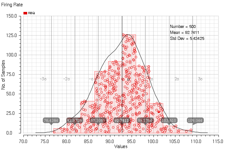
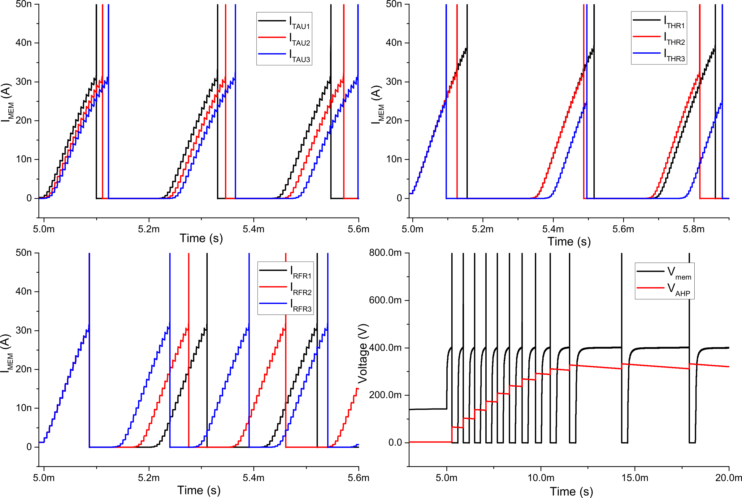
To minimize transistor mismatch effects, we identified the ones that are required to operate with small currents and assigned them large length values (e.g., , ). Even larger transistor sizes (e.g., ) were assigned key transistors relevant for mismatch (e.g., and ) . We performed Monte Carlo analysis with 500 runs for this neuron circuit, with DC current injected through , and with bias voltages set to obtain a firing rate of approximately 100 Hz. As shown in Fig. 3, for a mean firing rate of 92.7Hz, the standard deviation is 5.43 and error () is 5.86%.
Simulation results demonstrating examples of biologically plausible behaviors are shown in Fig.4. The top-left quadrant shows neuron membrane potential in response to a regular current spiking train for different leaking time constants (). The top-right quadrant shows the neuron response to a regular current spiking train injection for different values of firing threshold voltage (). The bottom-left quadrant shows the neuron response to a regular current spiking train injection for different settings of its refractory period (). The bottom-right quadrant demonstrates the spike-frequency adaptation behavior, obtained by appropriately tuning the relevant parameters in the AHP block of Fig. 2 and stimulating the neuron with a constant injection current.
With the transistor sizes chosen to minimize leakage current and device mismatch, the area of neuron, excluding the capacitor, is of approximately . The membrane capacitor can be overlayed onto the neuron layout using Metal Insulator Metal (MIM) structures. If we assume a capacitive density of approximately , the area required to implement sufficiently large capacitors (e.g. , and ) will be approximately .
II-B Asynchronous PCHB digital circuits
Pre-Charge Half-Buffer (PCHB)-based asynchronous AER routing/communication circuits are used to implement multi-core neuromorphic computing architectures. These circuits can be composed by combining basic building blocks that implement basic processes (merge, split, buffer, etc.), and that follow a standard 4-phase hand-shaking protocol.
Figure 5 shows an example of RTL level pipeline buffer following 4-phase handshaking protocol and dual-rail protocol based on PCHB. The process stage includes Handshaking, Validity and Buffer blocks. With dual-rail data protocol, the request signal from a previous stage is encoded in data, the Validity module checks the validity of input data and identifies the state via the signal . The handshaking block generates the acknowledge signal to acknowledge its previous stage for valid input. In parallel it will wait for the acknowledge signal from its following process stage, e.g. , for its valid output. While taking care of hand-shaking with neighbour stages, the handshaking block will generate control signal to enable Buffer block for dealing with current input data or reset the Buffer block for the next cycle (see Fig. 5).
Additional Quasi-Delay Insensitive (QDI) processes can be implemented with similar Handshaking, Validity and specific Function block. By using a dual-rail data flow and 4-phase handshaking, it is possible to build larger routing systems with more complex functions, properly placing and combining these concurrent processes.
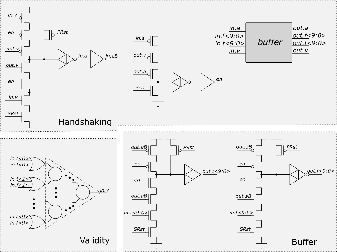
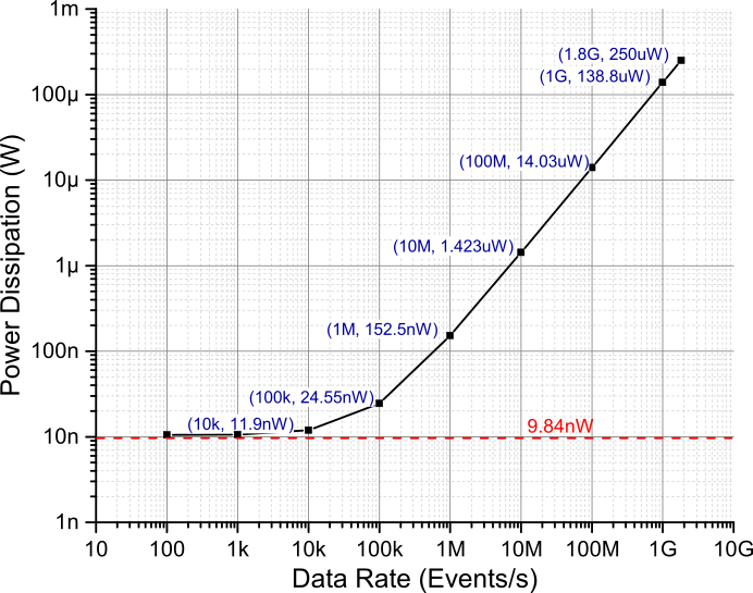
Figure 6 shows the power dissipation of a 10-bit PCHB-based buffer process versus different data rate of input events. The bandwidth of this 10-bit buffer is simulated to be 1.8 GEvents/s with a power dissipation of 250 uW. The power dissipation of this buffer stage will scale down linearly corresponding to lower data rate. For a small data rate, e.g lower than 100kEvents/s, the static power dissipation will play a role. For a data rate smaller than 1 kEvents/s, the mean power dissipation will be dominated by static power dissipation, which is 9.84 nW.
In case of implementing large enough asynchronous AER routing/communication system, according to estimates obtained from existing multi-core neuromorphic chips, the capacity of the whole asynchronous system will be equivalent of 600 10-bit buffers. In order to route 100 kEvents/s with this specific routing system, total power dissipation can be expected to be around 14.7 uW with 147 pJ per event.
II-C CAMs for implementing configurable digital synapses
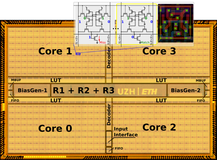
Figure 7 shows CAM cells that have been used to implement configurable digital synapses in previous 180 nm CMOS processes. The CAM cell considered is based on NOR-type 9T cells and utilize a pre-charge-high Match-Line (ML) scheme.
The layout of the CAM cell in 180 nm bulk CMOS process occupies an area of . With advanced 28 nm FPSOI process, it is reasonable to expect that the layout of CAM will be more compact with a silicon area smaller than , which will result in less than . If we assume a fan-in of 64 programmable synapse connections that feed into one neuron (e.g., to implement convolutional networks with 88 pixel kernels), and allocate 12-bits/synapse, the total silicon area that is expected to be used is , which is much larger than the area of the analog neuron (). Therefore the silicon area of the multi-core neuromorphic processor in 28 nm FD-SOI process following architecture would be dominated by the CAMs.
In Table I we compare features of multi-core neuromorphic processor with our old work in a 180 nm CMOS process and a neuromorphic system in a 28 nm CMOS process.
III Conclusion
In this paper we described some of the issues that have to be considered when scaling mixed-signal analog/digital neuromorphic circuits to advanced scaled process nodes. We showed how, by properly sizing the transistors of analog neurons, and by optimizing its layout, it is possible to obtain reliable operation in a 28 nm FD-SOI process, reducing both silicon area and power consumption. Furthermore, we showed that for asynchronous AER routing system, scaling to more advanced processes leads to a significant improvement in bandwidth, but not to improvements in area and power efficiency. This however can be potentially solved by resorting to integration of Resistive Random Access Memory (RRAM) elements on the same substrate.
| [9] | [10] | this work | |
|---|---|---|---|
| Technology | 180 nm CMOS | 28 nm CMOS | 28 nm FD-SOI |
| Supply voltage | 1.8V | 0.7V-1.0V | 1.0V |
| Energy per spike | 883pJ @ 30Hz | 2.3nJ-30nJ | 50pJ @ 30Hz |
| Energy per routing | 360pJ | 230pJ | 147pJ |
| Bandwidth of routers | 400MEvents/s | 20MEvents/s | 1.8GEvents/s |
| Area of neuron | 1188 | 64.6 | 20 |
| Area of synapse | 128.4 | 13 | 3 |
Acknowledgment
This work is supported by the EU ICT NeuRAM3 687299 grant.
References
- [1] Y. LeCun, Y. Bengio, and G. Hinton, “Deep learning,” Nature, vol. 521, no. 7553, pp. 436–444, 2015.
- [2] P. A. Merolla, J. V. Arthur, R. Alvarez-Icaza, A. S. Cassidy, J. Sawada, F. Akopyan, B. L. Jackson, N. Imam, C. Guo, Y. Nakamura, B. Brezzo, I. Vo, S. K. Esser, R. Appuswamy, B. Taba, A. Amir, M. D. Flickner, W. P. Risk, R. Manohar, and D. S. Modha, “A million spiking-neuron integrated circuit with a scalable communication network and interface,” Science, vol. 345, no. 6197, pp. 668–673, Aug. 2014. [Online]. Available: http://www.sciencemag.org/content/345/6197/668
- [3] B. V. Benjamin, P. Gao, E. McQuinn, S. Choudhary, A. R. Chandrasekaran, J. Bussat, R. Alvarez-Icaza, J. Arthur, P. Merolla, and K. Boahen, “Neurogrid: A mixed-analog-digital multichip system for large-scale neural simulations,” Proceedings of the IEEE, vol. 102, no. 5, pp. 699–716, 2014.
- [4] S. Furber, F. Galluppi, S. Temple, and L. Plana, “The SpiNNaker project,” Proceedings of the IEEE, vol. 102, no. 5, pp. 652–665, May 2014.
- [5] E. Chicca, F. Stefanini, C. Bartolozzi, and G. Indiveri, “Neuromorphic electronic circuits for building autonomous cognitive systems,” Proceedings of the IEEE, vol. 102, no. 9, pp. 1367–1388, Sep 2014. [Online]. Available: http://ncs.ethz.ch/pubs/pdf/Chicca_etal14.pdf
- [6] N. Qiao, H. Mostafa, F. Corradi, M. Osswald, F. Stefanini, D. Sumislawska, and G. Indiveri, “A re-configurable on-line learning spiking neuromorphic processor comprising 256 neurons and 128k synapses,” Frontiers in Neuroscience, vol. 9, no. 141, 2015. [Online]. Available: http://www.frontiersin.org/neuromorphic_engineering/10.3389/fnins.2015.00141/abstract
- [7] G. Indiveri and S.-C. Liu, “Memory and information processing in neuromorphic systems,” Proceedings of the IEEE, vol. 103, no. 8, pp. 1379–1397, 2015. [Online]. Available: http://ncs.ethz.ch/pubs/pdf/Indiveri_Liu15.pdf
- [8] S.-C. Liu, J. Kramer, G. Indiveri, T. Delbruck, and R. Douglas, Analog VLSI:Circuits and Principles. MIT Press, 2002. [Online]. Available: http://ncs.ethz.ch/pubs/pdf/Liu_etal02b.pdf
- [9] G. Indiveri, F. Corradi, and N. Qiao, “Neuromorphic architectures for spiking deep neural networks,” in Electron Devices Meeting (IEDM), 2015 IEEE International. IEEE, Dec. 2015, pp. 4.2.1–4.2.14. [Online]. Available: http://ncs.ethz.ch/pubs/pdf/Indiveri_etal15.pdf
- [10] C. Mayr, J. Partzsch, M. Noack, S. Hänzsche, S. Scholze, S. Höppner, G. Ellguth, and R. Schüffny, “A biological-realtime neuromorphic system in 28 nm cmos using low-leakage switched capacitor circuits,” IEEE transactions on biomedical circuits and systems, vol. 10, no. 1, pp. 243–254, 2016.