Efficiency enhancement of ultrathin CIGS solar cells by optimal bandgap grading
Faiz Ahmad1, Tom H. Anderson2, Peter B. Monk2, and Akhlesh Lakhtakia1
1Pennsylvania State University, Department of Engineering Science and Mechanics, NanoMM–Nanoengineered Metamaterials Group, University Park, PA 16802, USA
2University of Delaware, Department of Mathematical Sciences, 501 Ewing Hall, Newark, DE 19716, USA
Corresponding author: akhlesh@psu.edu
Abstract
The power conversion efficiency of an ultrathin CuIn1-ξGaξSe2 (CIGS) solar cell was maximized using a coupled optoelectronic model to determine the optimal bandgap grading of the nonhomogeneous CIGS layer in the thickness direction. The bandgap of the CIGS layer was either sinusoidally or linearly graded, and the solar cell was modeled to have a metallic backreflector corrugated periodically along a fixed direction in the plane. The model predicts that specially tailored bandgap grading can significantly improve the efficiency, with much smaller improvements due to the periodic corrugations. An efficiency of % with the conventional 2200-nm-thick CIGS layer is predicted with sinusoidal bandgap grading, in comparison to 22% efficiency obtained experimentally with homogeneous bandgap. Furthermore, the inclusion of sinusoidal grading increases the predicted efficiency to 22.89% with just a 600-nm-thick CIGS layer. These high efficiencies arise due to a large electron-hole-pair generation rate in the narrow-bandgap regions and the elevation of the open-circuit voltage due to a wider bandgap in the region toward the front surface of the CIGS layer. Thus, bandgap nonhomogeneity, in conjunction with periodic corrugation of the backreflector, can be effective in realizing ultrathin CIGS solar cells that can help overcome the scarcity of indium.
1 Introduction
The power conversion efficiency of thin-film CuIn1-ξGaξSe2 (CIGS) solar cells is about [1, 2]. This efficiency compares well to the 26.7% efficiency of single-junction crystalline-silicon solar cells [2], but the scarcity of indium is a major obstacle for large-scale and low-cost production of thin-film CIGS solar cells[3]. If the thickness of the CIGS layer could be reduced without significantly reducing the efficiency, this obstacle could be overcome. However, naïvely reducing that thickness below 1000 nm can lower for two reasons. First, the lower absorption of solar photons would reduce both the optical short-circuit current density and the open-circuit voltage . Second, the increased back-contact electron-hole-pair recombination rate [4, 5] would reduce the output current density. Common techniques under investigation to offset these problems include the use of light-trapping nanostructures [5, 6, 7], alternative back contacts [7], and back-surface passivation [8].
Although nonhomogeneity (i.e., bandgap grading) of the CIGS layer could increase by establishing drift fields [4], simple simulations as well as experiments have shown that linear grading of the bandgap can significantly reduce the short-circuit current density [4, 9, 10, 11]. New strategies are required for bandgap grading to maintain and enhance .
Optoelectronic simulations of thin-film Schottky-barrier solar cells with periodically nonhomogeneous absorbing layers of InGaAn and periodically corrugated backreflectors, predict improvement in efficiency [12, 13]. This improvement is due to: (i) the enhancement of owing to the excitation of guided wave modes by the use of the periodically corrugated backreflector [14, 15, 16, 17] and (ii) the enhancement of because of bandgap grading in the nonhomogeneous semiconductor layer [4, 11, 10]. Motivated by these simulations, we undertook a detailed optoelectronic optimization of ultrathin CIGS solar cells with a nonhomogeneous CIGS layer with back-surface passivation and backed by a periodically corrugated metallic backreflector.
Nonhomogeneity in the CIGS layer was modeled through either a sinusoidal or a linear variation of the bandgap along the thickness direction (taken to be the axis of a Cartesian coordinate system). The commonly considered planar molybdenum (Mo) contact, which also functions as a backreflector, was taken to be periodically corrugated along the axis for better light trapping [14, 16, 17]. Parenthetically, the replacement of Mo by silver (Ag) has been theoretically predicted to enhance [7], but the lower stability of Ag at temperatures exceeding 550 ∘C makes it impractical for the fabrication of CIGS solar cells. A thin passivation layer of was inserted between the CIGS layer and the backreflector. This passivation layer reduces the back-contact electron-hole recombination rate [8] and also protects the electrical characteristics of the CIGS layer [18].
We first used the rigorous coupled-wave approach (RCWA) [19, 20] to calculate the useful absorptance [21] of the chosen solar cell exposed to normally incident unpolarized light. Assuming the incident power spectrum was the AM1.5G solar spectrum [22], we then determined the -averaged electron-hole-pair generation rate in the solar cell. Then, we implemented the one-dimensional (1D) drift-diffusion model [18, 23] for electrical calculations. A hybridizable discontinuous Galerkin (HDG) scheme [24, 25] was developed for the drift-diffusion equations. The bandgap-dependent electron affinity and defect density [26] were incorporated in the electrical calculations, as also were the nonlinear Shockley–Read–Hall (SRH) and radiative electron-hole recombination processes [18, 23]. Surface recombination was neglected because it has been experimentally shown to be inconsequential for CIGS solar cells [27], but we did assess the role of traps at a CdS/CIGS interface in the solar cell [26] by incorporating a surface-defect layer [10]. The optoelectronic model was implemented for the conventional 2200-nm-thick homogeneous CIGS layer for and the predicted efficiency compared favorably with experimental results in the literature.
The bandgap profile of the CIGS layer and the dimensions of the backreflector were optimized for discrete values of the thickness of the CIGS layer ranging from 100 nm to 2200 nm. The differential evolution algorithm (DEA) [28] was used to maximize for three configurations:
-
(i)
homogeneous-bandgap CIGS layer with flat backreflector,
-
(ii)
sinusoidally nonhomogeneous-bandgap CIGS layer with periodically corrugated backreflector, and
-
(iii)
linearly nonhomogeneous-bandgap with periodically corrugated backreflector.
By implementing a coupled optoelectronic model instead of an optical model, we were able to bypass the major limitation of the latter: optical models can yield as well as the theoretical upper bound of the maximum extractable power density [29], but are incapable of accurately modeling and . Not surprisingly therefore, optical models yield homogeneous bandgap to be superior to bandgap grading for maximizing [30], but that conclusion is irrelevant for the maximization of , as we show in this paper.
The structure of this paper is as follows. Section 2 on optoelectronic optimization is divided into five subsections. The optical description of the solar cell is presented in Sec 2.2.1 and the approach adopted for optical calculations is summarized in Sec. 2.2.2, the electrical description of the solar cell is discussed in Sec 2.2.3 and the equations solved are described in Sec. 2.2.4, and optimization is discussed in Sec. 2.2.5.
Numerical results are presented and discussed in Sec. 3, which is divided into seven subsections. Section 3.3.1 compares the efficiency of the conventional 2200-nm-thick solar cell with a homogeneous CIGS layer predicted by the model with available experimental data. The effect of the passivation layer on the solar-cell performance is discussed in Sec. 3.3.2. Section 3.3.3 provides the optimal results for solar cells with a homogeneous CIGS layer and a flat backreflector, Sec. 3.3.4 for solar cells with a homogeneous CIGS layer and a periodically corrugated backreflector, and Sec. 3.3.5 for solar cells with a linearly graded CIGS layer and a periodically corrugated backreflector. Optimal results for solar cells with a sinusoidally graded CIGS layer and a periodically corrugated backreflector are discussed in Sec. 3.3.6. A detailed study of the optimal 600-nm-thick solar cell is presented in Sec. 3.3.7. The paper ends with concluding remarks in Sec. 4.
All optical calculations were performed with an implicit dependence on time , with as the angular frequency and . The free-space wavelength and the intrinsic impedance of free space are denoted by and , respectively, where is the free-space wavelength, is the permeability of free space, is the permittivity of free space, and is the speed of light in free space. Vectors are underlined and the Cartesian unit vectors are identified as , , and .
2 Optoelectronic optimization
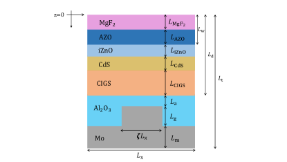
The structure of the CIGS solar cell is shown schematically in Fig. 1. The solar cell occupies the region , with the half spaces and occupied by air. The reference unit cell of this structure is identified as , with the backreflector being periodically corrugated with period along the axis.
The window region nm consists of a 110-nm-thick layer of magnesium fluoride (MgF2) [31] as an antireflection coating [32] and a 100-nm-thick layer of aluminum-doped zinc oxide (AZO) [33] as an electrical contact. The region is a 80-nm-thick layer of intrinsic zinc oxide (iZnO) [34] as a buffer layer to increase the open-circuit voltage [35]. The region is a 70-nm-thick layer of -type CdS [36] to form a junction with a -type CIGS layer of thickness nm.
The region of thickness nm is occupied by [37]. This is included to protect the electrical characteristics of the CIGS layer and also function as a passivation layer to reduce the back-surface electron-hole recombination rate. The region is occupied by Mo [38], the thickness nm being chosen to be well beyond the electromagnetic penetration depth [39] of Mo in the optical regime. The region consists of a rectangular Mo grating with period along the axis.
2.1 Optical description of solar cell
The permittivity in the grating region of is given by
| (3) | |||
| (4) |
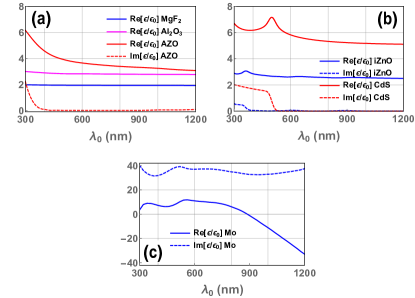
where is the duty cycle, is the permittivity of Mo [38], and is the permittivity of [33]. Spectrums of real and imaginary parts of the relative permittivity of MgF2 [31], AZO [33], iZnO [34], CdS [36], [37], and Mo [38] used in our calculations are displayed in Fig. 2.
The bandgap of CIGS varies with in the CIGS layer. As solar cells are fabricated using vapor-deposition techniques [40], nonhomogeneous bandgap profiles could be physically realized by varying the parameter during the deposition process [26, 41]. The linearly nonhomogeneous bandgap for forward grading was modeled as
| (5) |
where is the minimum bandgap, is the maximum bandgap, and is an amplitude (with representing a homogeneous CIGS layer). The linearly nonhomogeneous bandgap for backward grading was modeled as
| (6) |
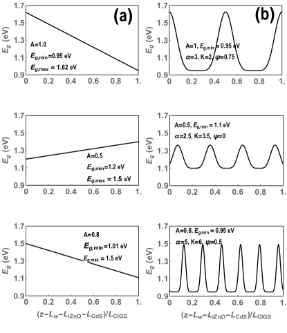
Three representative profiles of linearly nonhomogeneous bandgap are shown in Fig. 3(a). The parameter space for optimization of was fixed as follows: , , , , eV, and eV with the condition .
The sinusoidally varying bandgap was modeled as
| (7) |
where quantifies a relative phase shift, is the number of periods in the CIGS layer, and is a shaping parameter. Three representative profiles of sinusoidally nonhomogeneous bandgap are shown in Fig. 3(b). The parameter space for optimization of was fixed as follows: , , , , , , , and .
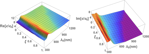
Spectrums of the real and imaginary parts of the relative permittivity of CIGS in the optical regime are plotted in Fig. 4 as functions of [30, 42].
2.2 Optical calculations
The RCWA [19, 20] was used the calculate the electric field phasor everywhere inside the solar cell as a result of illumination by a monochromatic plane wave normally incident on the plane from the half space . The electric field phasor of the incident plane wave was taken as
| (8) |
where V m-1. The region was partitioned into a sufficiently large number of slices along the axis, such that the useful solar absorptance [21, 30] converged correct to . Each slice was taken to be homogeneous along the axis but could be periodically nonhomogeneous along the axis. Standard boundary conditions were enforced on the planes and to match the internal field phasors to the incident, reflected, and transmitted field phasors, as appropriate. Detailed descriptions of the RCWA implementation are available elsewhere [30, 20, 13].
With the assumption that every absorbed photon excites an electron-hole pair, the electron-hole-pair generation rate was calculated as
| (9) |
for , where is the reduced Planck constant, is the AM1.5G solar spectrum [22], nm, and eV nm. As the solar cell operates under the influence of a -directed electrostatic field created by the application of a bias voltage , charge carriers generally flow along the axis, any current generated parallel to the axis being very small. Moreover, the period of the corrugated backreflector is 500 nm, which is so small in comparison to the lateral dimensions of the solar cell that it can be ignored for electrostatic analysis. Therefore, the -averaged electron-hole-pair generation rate was calculated as
| (10) |
for use in Secs. 2.2.3 and 2.2.4. The generation rate contains the effects of: (i) the periodic corrugations of the backreflector, (ii) the back-surface passivation layer, and (iii) the MgF2 antireflection coating.
2.3 Electrical description of solar cell
The region containing the iZnO, CdS, and CIGS layers was considered for electrical modeling. Both iZnO and CdS must be considered in addition to CIGS, because both contribute to charge-carrier generation. The useful solar spectrum is typically taken to span free-space wavelengths in excess of nm. Since iZnO has a bandgap of 3.3 eV, it will absorb solar photons with energies corresponding to nm. Likewise, as CdS has a bandgap of 2.4 eV, it will absorb solar photons with energies corresponding to nm. Hence, the generation of electron-hole pairs in the iZnO and CdS layers must be accounted for, not to mention the recombination of electron-hole pairs in both layers.
As our focus is on modeling the electrical characteristics of the solar cell, not on how it interfaces with an external circuit, both terminals were assumed to be ideal ohmic contacts. We used a 1D drift-diffusion model [23, 18, 43] to investigate the transport of electrons and holes for , as discussed next.
2.4 Electrical theory
The electron-current density and the hole-current density are driven by gradients in the electron and hole quasi-Fermi levels, respectively. Thus [23, Sec. 4.6],
| (11) |
where 10-19 C is the elementary charge; and are the electron density and hole density, respectively; and and are the electron mobility and hole mobility, respectively. The electron quasi-Fermi level
| (12) |
and the hole quasi-Fermi level
| (13) |
involve the product of the Boltzmann constant J K-1 and the absolute temperature . Furthermore, is the density of states in the conduction band, is the density of states in the valence band, is the conduction band-edge energy, is the valence band-edge energy, is the dc electric potential, and is the bandgap-dependent electron affinity. The reference energy level is arbitary. When the right side of Eq. (12) is substituted in Eq. (11)1, the contribution of diffusion of electrons to can be identified as depending on , the remainder being the contribution of electron drift; and likewise for .
According to the Boltzmann approximation [23],
| (14) |
where the intrinsic charge-carrier density
| (15) |
and the intrinsic energy
| (16) |
Under steady-state conditions, the 1D drift-diffusion model comprises the following three differential equations [23, Sec. 4.6]:
| (17) | ||||
| (18) | ||||
| (19) |
These differential equations hold for , with as the electron-hole-pair recombination rate, as the defect density (also called trap density), as the donor density which is positive for donors and negative for acceptors, and as the dc relative permittivity. Although , , and depend on because they depend on the bandgap, following Frisk et al. [26] we took all three quantities to be independent of because bandgap-dependent values are not available for CIGS.
Electron-hole pairs are produced at the rate defined in Eq. (10) and recombine at the rate . We incorporated the radiative recombination and SRH recombination processes via [23, 18]. The radiative recombination rate is given by
| (20) |
where is the radiative recombination coefficient. The SRH recombination rate is given by
| (21) |
where and are the electron and hole densities at the trap energy level ; the minority carrier lifetimes
| (22) |
depend on the capture cross sections and for electrons and holes, respectively; and represents the mean thermal speed for all charge carriers. The defect density was taken to be bandgap-dependent for the SRH recombination rate. Equation (19) describes the dc electric potential created by the electrically charged regions of the solar cell. Table 1 provides the values of the aforementioned electrical parameters as well as the doping density used for iZnO, CdS, and CIGS [26].
Equations (17)–(19) were supplemented by Dirichlet boundary conditions on , , and at the planes and [13, 44]. These boundary conditions were derived after assuming the region to be uncharged and at local quasi-thermal equilibrium [18]; furthermore, a bias voltage was applied at the plane . Solution of this system of equations was undertaken using the HDG scheme [46, 25, 45], in which all the -dependent variables have to be discretized using discontinuous finite elements in a space of piecewise polynomials of a fixed degree. The full discretized system was solved for , , and , using the Newton–Raphson method [43]. The HDG scheme is particularly advantageous for simulating solar cells with heterojunction interfaces [47] such as those which occur between the CdS and CIGS layers.
| Parameter (unit) | iZnO | CdS | CIGS |
| (eV) | 3.3 | – (Ga-dependent) | |
| (eV) | 4.4 | – (Ga-dependent) | |
| (cm-3) | |||
| (cm-3) | |||
| (cm-3) | (donor) | (donor) | (acceptor) |
| (cm2 | |||
| V-1 s-1) | |||
| (cm2 | |||
| V-1 s-1) | |||
| (cm-3) | – (Ga-dependent) | ||
| midgap | midgap | midgap | |
| (cm2) | |||
| (cm2) | |||
| (cm3 | |||
| s-1) | |||
| (cm s-1) |
2.5 Optoelectronic optimization
Solution of the drift-diffusion equations enabled the calculation of the current density
| (23) |
flowing through the iZnO/CdS/CIGS region. Under steady-state conditions, is constant throughout the solar cell. Thus, is the current density delivered to an external circuit; is the value of when and is the value of such that . With the power density defined as , the maximum power density obtainable from the solar cell is the highest point on the - curve. The efficiency is calculated as the ratio , where W m-2 is the integral of over the solar spectrum. Also, a figure of merit called fill factor is commonly considered in solar-cell research. The DEA [28] was used to optimize , using a custom algorithm implemented with MATLAB® version R2017b.
3 Numerical results and discussion
3.1 Conventional CIGS solar cell (model validation)
First, we validated our coupled optoelectronic model by comparison with extant experimental results for the conventional MgF2/AZO/iZnO/CdS/CIGS/Mo solar cell containing a 2200-nm-thick homogeneous CIGS layer and a flat backreflector [48]. Values of , , , and obtained from our model for ( eV), ( eV), and ( eV) are provided in Table 2, as also are the corresponding experimental data [1, 48]. The model predictions are in reasonable agreement with the experimental data, the differences very likely due to variance between the optical and electrical properties used in the model from those realized in practice.
| (eV) | (mA | (mV) | (%) | (%) | ||
| cm | ||||||
| 0 | 0.95 | Model | 38.63 | 497 | 78 | 15.05 |
| Experiment | ||||||
| (Ref. [48]) | 40.58 | 491 | 66 | 14.5 | ||
| Experiment | ||||||
| (Ref. [48]) | 41.1 | 491 | 75 | 15.0 | ||
| 0.25 | 1.12 | Model | 34.41 | 648 | 81 | 18.12 |
| Experiment | ||||||
| (Ref. [48]) | 35.22 | 692 | 79 | 19.5 | ||
| Experiment | ||||||
| (Ref. [1]) | 37.8 | 741 | 81 | 22.6 | ||
| 1 | 1.626 | Model | 14.86 | 911 | 73 | 9.92 |
| Experiment | ||||||
| (Ref. [48]) | 14.88 | 823 | 71 | 9.53 | ||
| Experiment | ||||||
| (Ref. [48]) | 18.61 | 905 | 75 | 10.2 |
Next, we assessed the role of traps at the CdS/CIGS interface in the solar cell [26] by incorporating a 10-nm-thick surface-defect layer between the CdS and the CIGS layers [10]. The interface trap density was taken to be cm-2, all other characteristics of the surface-defect layer being the same as of the CIGS layer [26]. The efficiency reduced in consequence, but the reduction was very small. For example, the efficiency calculated for reduced from 18.12% (Table 2) to 18.11%. This is accord with an experimental study concluding the influence of surface recombination on high-efficiency CIGS solar cells to be insignificant [27]. We ignored the surface-defect layer for all results presented from hereonwards in this paper.
3.2 Effect of layer
To delineate the effect of the 50-nm-thick layer between the CIGS layer and a flat backreflector, we optimized the CIGS solar cell with and without that layer. Values of , , , and obtained from our model for nm are presented in Table 3. The optimal efficiency is % with the layer and % without it. Surface recombination being insignificant [27], the %-enhancement of is very likely due to the reduction of optical mismatch between Mo and CIGS by the layer. Improvements in both short-circuit current density and open-circuit voltage due to the layer can also be noted in Table 3. Hence, the 50-nm-thick layer is present in the solar cell for all results presented from now onward.
| (nm) | (eV) | (mA | (mV) | (%) | (%) |
| cm | |||||
| 0 | 1.27 | 21.63 | 705 | 77 | 11.88 |
| 50 | 1.27 | 22.65 | 711 | 77 | 12.49 |
3.3 Optimal solar cell: Homogeneous bandgap & flat backreflector
To allow comparison with a sensible baseline and highlight the advantages of the proposed designs, it is useful to run the optoelectronic optimization for a CIGS solar cell in which the bandgap is homogeneous and the backreflector is flat; i.e., and . The parameter space for optimizing then reduces to: eV.
Values of , , , and [18, 23] corresponding to the optimal design for nm are shown in Table 4. Depending on , the optimal homogeneous bandgap varies, with eV. The optimal efficiency increases with . An efficiency of 13.79% is predicted with an ultrathin-600-nm CIGS layer. The highest efficiency predicted is %, for a solar cell with a 2200-nm-thick CIGS layer with an optimal bandgap of eV.
| (nm) | (eV) | (mA | (mV) | (%) | (%) |
| cm | |||||
| 100 | 1.28 | 14.89 | 624 | 78 | 7.25 |
| 200 | 1.26 | 19.50 | 660 | 76 | 9.76 |
| 300 | 1.25 | 22.56 | 681 | 76 | 11.59 |
| 400 | 1.27 | 22.65 | 711 | 77 | 12.49 |
| 500 | 1.25 | 23.71 | 704 | 78 | 13.15 |
| 600 | 1.24 | 24.66 | 704 | 79 | 13.79 |
| 900 | 1.25 | 25.68 | 725 | 80 | 15.08 |
| 1200 | 1.28 | 25.72 | 756 | 81 | 15.90 |
| 2200 | 1.24 | 31.11 | 742 | 82 | 18.93 |
| (nm) | (eV) | (nm) | (nm) | (mA | (mV) | (%) | (%) | |
| cm-2) | ||||||||
| 100 | 1.28 | 500 | 0.50 | 97 | 14.89 | 624 | 78 | 7.25 |
| 200 | 1.26 | 510 | 0.50 | 101 | 19.53 | 661 | 76 | 9.91 |
| 300 | 1.25 | 510 | 0.50 | 101 | 22.56 | 681 | 76 | 11.59 |
| 400 | 1.27 | 510 | 0.49 | 101 | 22.79 | 711 | 77 | 12.58 |
| 500 | 1.25 | 510 | 0.48 | 106 | 23.78 | 705 | 78 | 13.19 |
| 600 | 1.24 | 510 | 0.48 | 105 | 24.69 | 704 | 79 | 13.81 |
| 900 | 1.25 | 502 | 0.49 | 101 | 25.71 | 725 | 80 | 15.09 |
| 1200 | 1.28 | 502 | 0.49 | 101 | 25.72 | 759 | 81 | 15.90 |
| 2200 | 1.24 | 502 | 0.49 | 101 | 31.11 | 742 | 82 | 18.93 |
3.4 Optimal solar cell: Homogeneous bandgap & periodically corrugated backreflector
Next, we repeated optoelectronic optimization for solar cells containing a homogeneous CIGS layer but with a periodically corrugated backreflector instead of a flat one. The results of this optimization exercise for fixed are provided in Table 5. On comparing Tables 4 and 5, we see that periodic corrugation of the Mo backreflector improves the efficiency by no more than % (at nm). This indicates the moderate benefit of exciting both surface-plasmon-polariton (SPP) waves [49, 50] and waveguide modes [17] by taking advantage of the grating-coupled configuration [20], when the CIGS layer is ultrathin. However, that benefit vanishes for thicker CIGS layers.
3.5 Optimal solar cell: Linearly nonhomogeneous bandgap
Next, let us consider the maximization of as a function of when the CIGS layer has a linearly nonhomogeneous bandgap, according to either Eq. (5) or Eq. (6).
3.5.1 Forward grading
Equation (5) is used for linearly nonhomogeneous forward bandgap grading, so that for , the bandgap being smaller near the front contact than near the back contact. Optoelectronic optimization yielded . Thus, for forward bandgap grading of the CIGS layer, Table 4 holds when the backreflector is flat and Table 5 holds when the backreflector is periodically corrugated.
3.5.2 Backward grading
When Eq. (5) is replaced by Eq. (6) so that for , optoelectronic optimization predicts for optimal efficiency.
Table 6 presents optimal for nine values of , when the CIGS bandgap is linearly nonhomogeneous according to Eq. (6) and the Mo backreflector is periodically corrugated. For nm, the optimal % in Table 6, whereas % in Table 4. This relative enhancement of % must be attributed to the backward bandgap grading of the CIGS layer. Concurrently, increases from mW cm-2 to mA cm-2 (% relative increase) and from mV to mV (% relative increase); however, the fill factor reduces from % to %.
The overall trend encompasses the enhancement of both and and the reduction of and FF with backward bandgap grading for all considered thicknesses of the CIGS layer. For nm, upon the incorporation of a linearly nonhomogeneous bandgap and a periodically corrugated backreflector, the optimal efficiency increases from % (Table 4) by % to % (Table 6) and increases from mV by % to mV, but decreases from mA cm-2 by % to mA cm-2 and the fill factor reduces from % to %. The relative enhancement in efficiency decreases as increases. Thus, the relative enhancement is only % for nm. Higher values of are positively correlated with larger values of .
| A | ||||||||||
| (nm) | (eV) | (eV) | (nm) | (nm) | (mA cm-2) | (mV) | (%) | (%) | ||
| 100 | 1.61 | 0.96 | 0.98 | 500 | 0.50 | 97 | 15.09 | 960 | 68 | 9.88 |
| 200 | 1.61 | 0.96 | 0.98 | 510 | 0.51 | 101 | 19.28 | 995 | 62 | 12.08 |
| 300 | 1.62 | 0.96 | 0.98 | 502 | 0.49 | 101 | 20.70 | 1010 | 63 | 13.34 |
| 400 | 1.62 | 0.96 | 0.98 | 510 | 0.49 | 101 | 21.13 | 1011 | 67 | 14.34 |
| 500 | 1.62 | 0.95 | 0.99 | 510 | 0.48 | 106 | 21.31 | 1017 | 69 | 15.14 |
| 600 | 1.62 | 0.95 | 0.75 | 500 | 0.50 | 101 | 21.48 | 1023 | 71 | 15.79 |
| 900 | 1.62 | 0.95 | 0.75 | 500 | 0.50 | 101 | 22.21 | 1032 | 75 | 17.24 |
| 1200 | 1.62 | 0.95 | 0.75 | 500 | 0.50 | 101 | 22.74 | 1037 | 76 | 18.07 |
| 2200 | 1.62 | 0.95 | 0.75 | 500 | 0.50 | 101 | 24.09 | 1039 | 77 | 19.27 |
3.6 Optimal solar cell: Sinusoidally nonhomogeneous bandgap & periodically corrugated backreflector
Next, let us consider the optoelectronic optimization of for fixed values of for a solar cell with a periodically nonhomogeneous CIGS layer according to Eq. (7) and a periodically corrugated backreflector. Values of optimized for fixed are shown in Table 7. Values of , , , , , , , , , , and for the optimal designs are also shown in this table.
For nm, the optimal efficiency is % in Table 7, a relative increase of % over the optimal efficiency of % in Table 4. This enhancement must be due to the sinusoidally nonhomogeneous bandgap. Concurrently, increases from mA cm-2 to mA cm-2 (% relative increase) and from mV to mV (% relative increase); however, the fill factor reduces from % to %. Notably, increased significantly without decreasing, which is in contrast to solar cells with either a homogeneous or a linearly nonhomogeneous CIGS layer [4, 10].
For nm, upon the incorporation of a sinusoidally nonhomogeneous bandgap and a periodically corrugated backreflector, the optimal efficiency increases from % (Table 4) by % to % (Table 7), increases mA cm-2 by % to mA cm-2, and from mV by % to mV, but the fill factor reduces from % to %. Likewise, for nm, the optimal efficiency increases by % to % from , increases by % to mA cm-2 from mA cm-2, and increases by % to mV from mV, although the fill factor reduces to % from %. The overall trend is that the relative enhancement of —due to the sinusoidally nonhomogeneous bandgap and the periodically corrugated banckreflector—decreases with the increase of , on optoelectronic optimization. The highest optimal % in Table 7 was obtained with the conventional 2200-nm-thick CIGS layer, a relative enhancement of % with respect to % for the homogeneous CIGS layer in Table 4. The short-circuit current density increases from mA cm-2 by % to mA cm-2, increases from mV by % to mV, but the fill factor reduces to % from %.
Optimal values of range from to in Table 7, which is in contrast to delivered by optical optimization of [21]. The maximum value of provides the largest possible bandgap variation in the nonhomogeneous CIGS layer. Thus, optoelectronic optimization delivers sinusoidal nonhomogeneity of the bandgap with a large amplitude, whereas optical optimization severely suppresses nonhomogeneity of the bandgap. The inescapable conclusions are that (i) optical optimization is seriously deficient and (ii) optoelectronic optimization is essential for nonhomogeneous-bandgap solar cells.
Previous studies on Schottky-barrier thin-film solar cells [12, 13] had suggested that optimal values of are integer multiples of and that . Both predictions are mostly upheld by the optimal data in Table 7.
The relative enhancement in is almost the same for linear bandgap grading (Table 6) as for sinusoidal bandgap grading (Table 7) of the CIGS layer in comparison to the homogenous CIGS layer (Tables 4 and 5). However, whereas sinusoidal bandgap grading of the CIGS layer enhances , linear bandgap grading of that layer actually depresses , in comparison to the homogeneous CIGS layer. As the reduction of does not completely overcome the enhancement of for linear bandgap grading, the efficiencies in Table 6 exceed their counterparts in Tables 4 and 5; of course, the efficiencies in Table 7 are even higher. We conclude that sinusoidally nonhomogeneous bandgap is more efficient than the homogeneous and the linearly nonhomogeneous bandgaps for all nm.
| A | ||||||||||||
| (nm) | (eV) | (nm) | (nm) | (mA | (mV) | (%) | (%) | |||||
| cm-2) | ||||||||||||
| 100 | 0.96 | 0.99 | 6.14 | 0.75 | 0.75 | 510 | 0.50 | 101 | 17.04 | 969 | 71 | 12.37 |
| 200 | 0.95 | 1.00 | 6.0 | 1.50 | 0.75 | 500 | 0.48 | 101 | 24.12 | 1007 | 69 | 16.89 |
| 300 | 0.95 | 0.98 | 6.0 | 1.50 | 0.74 | 502 | 0.49 | 101 | 25.98 | 1023 | 71 | 19.01 |
| 400 | 0.95 | 0.98 | 6.0 | 1.50 | 0.75 | 500 | 0.50 | 111 | 27.17 | 1033 | 73 | 20.66 |
| 500 | 0.95 | 0.99 | 6.0 | 1.50 | 0.76 | 520 | 0.50 | 111 | 28.23 | 1040 | 74 | 21.90 |
| 600 | 0.95 | 0.99 | 6.0 | 1.50 | 0.75 | 510 | 0.48 | 106 | 29.18 | 1045 | 75 | 22.89 |
| 900 | 0.95 | 0.99 | 6.0 | 1.50 | 0.75 | 510 | 0.48 | 106 | 30.86 | 1057 | 76 | 24.98 |
| 1200 | 0.95 | 0.98 | 6.0 | 1.50 | 0.75 | 510 | 0.48 | 106 | 32.02 | 1063 | 77 | 26.33 |
| 2200 | 0.95 | 0.98 | 6.0 | 1.50 | 0.75 | 510 | 0.48 | 106 | 33.16 | 1070 | 78 | 27.70 |
3.7 Optimal solar cells with 600-nm-ultrathin CIGS layer
The highest efficiency in Tables 4–7 is 27.7%. It is predicted by our coupled optoelectronic model for the CIGS solar cell with a sinusoidally nonhomogeneous 2200-nm-thick CIGS layer. However, we are interested in ultrathin CIGS layers to reduce the material and processing costs, keeping in mind the scarcity of indium. The solar cell with the sinusoidally nonhomogeneous CIGS layer of 600-nm thickness and a periodically corrugated Mo backreflector has efficiency which compares well with the efficiency of the conventional CIGS solar cell with a 2200-nm-thick homogeneous CIGS layer [1]. Therefore, a detailed study of the solar cell with the 600-nm-thick nonhomogeneous CIGS layer is reported next.
3.7.1 Backward linearly nonhomogeneous bandgap
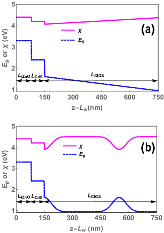
The design and performance parameters of the optimal CIGS solar cell with a 600-nm-thick linearly nonhomogeneous CIGS layer are provided in Table 6. Spatial profiles of and delivered by optoelectronic optimization are provided in Fig. 5(a).
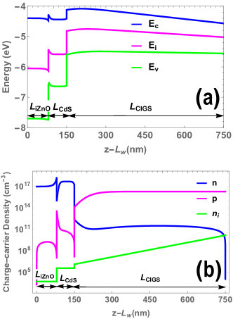
Figure 6(a) presents the spatial profiles of , , and . The spatial variations of and are similar to that of and provide the conditions to enhance the generation rate [4]. Figure 6(b) presents the graphs of , , and under the equilibrium condition. The intrinsic carrier density varies linearly such that it is small where is large and vice versa.
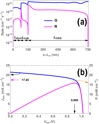
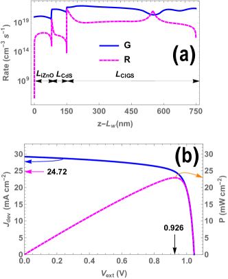
Spatial profiles of and are given in Fig. 7(a). The generation rate is higher near the front face and the back face of the CIGS layer and slightly lower in the middle of that layer, but the recombination rate drops sharply near the back face of that layer. Furthermore, the spatial profile of the recombination rate follows that of the defect density (not provided here). The - characteristics of the solar cell are shown in Fig. 7(b). From this figure, mA cm-2, V, %, and % for the best performance.
3.7.2 Sinusoidally nonhomogeneous bandgap & periodically corrugated backreflector
The parameters of the optimal CIGS solar cell with a 600-nm-thick sinusoidally nonhomogeneous CIGS layer are provided in Table 7. The variations of and with in the iZnO/CdS/CIGS region of the ultrathin CIGS solar cell are depicted in Fig. 5(b). With eV and , eV. The magnitude of is large in the proximity of the plane , which elevates . The regions in which is small are of substantial thickness, these regions being responsible for elevating the electron-hole-pair generation rate [18]. The sinusoidal grading close to the back-surface adds additional drift field to reduce the back-surface recombination rate, supplementing the role of the passivation layer. Thus the bandgap profile is ideal for high efficiency.
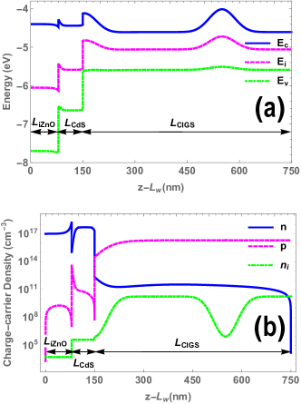
Figure 8(a) shows the variations of , , and with respect to . The spatial profiles of and are similar to that of and provide the conditions to enhance the generation rate [4]. Figure 8(b) shows the spatial variations of the electron, hole and intrinsic carrier densities under equilibrium condition. The holes are the majority carriers in -type CIGS and electrons are the majority carriers in -type CdS. The intrinsic carrier density varies sinusoidally such that is small where is large and vice versa.
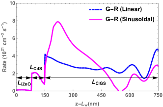
Profiles of the electron-hole-pair generation rate and recombination rate are shown in Fig. 9(a). The generation rate is higher in regions with lower bandgap and vice versa. Higher electron-hole-pair generation rate in the proximity of the plane can be seen as a consequence of the enhanced electric field at optical frequencies due to the excitation of SPP waves near the back face of the CIGS layer facilitated by the periodically corrugated backreflector [49, 50, 52, 51, 15].
The - characteristics of the solar cell are shown in Fig. 9(b). Our optoelectronic model predicts mA cm-2, V, %, and % for the best performance of this solar cell. Given that the thickness of the CIGS layer is just nm, this value of efficiency compares favorably with the % efficiency reported for solar cells with a -nm-thick homogeneous CIGS layer [1, 2].
3.7.3 Sinusoidally nonhomogeneous bandgap vs. linearly nonhomogeneous bandgap
When the bandgap is sinusoidally graded in the CIGS layer, the electron-hole-pair generation rate is higher in the small-bandgap regions than elsewhere in the CIGS layer. The open-circuit voltage is elevated in the optoelectronically optimal designs, because the bandgap is high in the proximity of both faces of the CIGS layer [13, 4, 11]. Both of these features help increase the efficiency, as discussed in Sec. 3.3.7.2.
Similar conclusions emerge when the bandgap is linearly graded in the CIGS layer, with the bandgap being smaller near the back face than near the front face. However, Fig. 5(b) shows that the bandgap is flat and low (1 eV) in a large portion of the CIGS layer when the bandgap is sinusoidally nonhomogenous, but that feature is missing in Fig. 5(a) for the linearly nonhomogeneous CIGS layer. The spatial profiles of provided in Fig. 10 confirm that the net production of charge carriers is boosted in regions of uniformly low bandgap. Hence, the efficiency is significantly higher for sinusoidal grading () than for linear grading () of the bandgap in the CIGS layer.
4 Concluding remarks
Optoelectronic optimization was carried out for an ultrathin CuIn1-ξGaξSe2 solar cell with: (i) a CIGS layer that is nonhomogeneous along the thickness direction and (ii) a metallic backreflector corrugated periodically along a fixed direction. The bandgap in the CIGS layer was either sinusoidally or linearly graded.
A % efficiency, mA cm-2 short-circuit current density, mV open-circuit voltage, and % fill factor can be achieved with a 2200-nm-thick CIGS layer that is sinusoidally graded and is accompanied by a periodically corrugated Mo backreflector. There is no change in the foregoing data if the corrugations of the backreflector are suppressed. In comparison, the efficiency is %, the short-circuit current density is mA cm-2, the open-circuit voltage is mV, and the fill factor is %, when the bandgap is homogeneous and the backreflector is flat.
In addition, a % efficiency, mA cm-2 short-circuit current density, mV open-circuit voltage, and % fill factor can be achieved with a 600-nm-thick CIGS layer that is sinusoidally nonhomogeneous and is accompanied by a periodically corrugated Mo backreflector. The efficiency reduces to % is the backreflector is flat, indicating the modest role of SPP waves [49, 50] and waveguide modes [17] for efficiency enhancement when the CIGS layer is ultrathin. In comparison, the efficiency is %, the short-circuit current density is mA cm-2, the open-circuit voltage is mV, and the fill factor is % when the CIGS layer is homogeneous and the backreflector is flat. The periodic corrugation of the backreflector explains some of the enhancement of efficiency, but the majority of the enhancement is seen to be driven by the bandgap nonhomogeneity. Efficiency enhancement can also be achieved by linearly grading the bandgap, but the gain is significantly smaller.
Optoelectronic optimization thus indicates that % efficiency is achievable with ultrathin solar cells with a 600-nm-thick CIGS layer. This efficiency compares favorably with the 22% efficiency demonstrated with CIGS layers that are more than three times thicker. Thus, bandgap nonhomogeneity in conjunction with periodic corrugation of the backreflector can be effective in realizing ultrathin CIGS solar cells that can help us in tackling the scarcity of indium and provide a way towards multi-terawatt solar-power production. We hope that our model-predicted results will provide an impetus to devise efficacious techniques for bandgap grading of ultrathin CIGS layers.
Acknowledgments. The authors thank two anonymous reviewers for invaluable suggestions to improve the contents of this paper. A. Lakhtakia thanks the Charles Godfrey Binder Endowment at the Pennsylvania State University for ongoing support of his research. The research of F. Ahmad and A. Lakhtakia was partially supported by US National Science Foundation (NSF) under grant number DMS-1619901. The research of T. H. Anderson and P. B. Monk was partially supported by the US NSF under grant number DMS-1619904.
References
- [1] P. Jackson, R. Wuerz, D. Hariskos, E. Lotter, W. Witte, and M. Powalla, “Effects of heavy alkali elements in Cu(In,Ga)Se2 solar cells with efficiencies up to 22.6%,” Phys. Status Solidi RRL 10, 583–586 (2016).
- [2] M. A. Green, Y. Hishikawa, E. D. Dunlop, D. H. Levi, J. Hohl-Ebinger, and A. W. Y. Ho-Baillie, “Solar cell efficiency tables (version 51),” Prog. Photovolt.: Res. Appl. 26, 3–12 (2018).
- [3] C. Candelise, M. Winskel, and R. Gross, “Implications for CdTe and CIGS technologies production costs of indium and tellurium scarcity,” Prog. Photovolt: Res. Appl. 20, 816–831 (2012).
- [4] M. Gloeckler and J. R. Sites, “Potential of submicrometer thickness Cu(In,Ga)Se2 solar cells,” J. Appl. Phys. 98, 103703 (2005).
- [5] M. Schmid, “Review on light management by nanostructures in chalcopyrite solar cells,” Semicond. Sci. Technol. 32, 043003 (2017).
- [6] C. van Lare, G. Yin, A. Polman, and M. Schmid, “Light coupling and trapping in ultrathin Cu(In,Ga)Se2 solar cells using dielectric scattering patterns,” ACS Nano 9(10), 9603–9613 (2015).
- [7] J. Goffard, C. Colin, F. Mollica, A. Cattoni, C. Sauvan, P. Lalanne, J.-F. Guillemoles, N. Naghavi, and S. Collin, “Light trapping in ultrathin CIGS solar cells with nanostructured back mirrors,” IEEE J. Photovolt. 7, 1433–1441 (2017).
- [8] B. Vermang, J. T. Wätjen, V. Fjällström, F. Rostvall, M. Edoff, R. Kotipalli, F. Henry, and D. Flandre, “Employing Si solar cell technology to increase efficiency of ultra-thin Cu(In,Ga)Se2 solar cells,” Prog. Photovolt: Res. Appl. 22, 1023–1029 (2014).
- [9] M. Gloeckler and J. R. Sites, “Band-gap grading in Cu(In,Ga)Se2 solar cells,” J. Phys. Chem. Solids 66, 1891-1894 (2005).
- [10] J. Song, S. S. Li, C. H. Huang, O. D. Crisalle, and T. J. Anderson, “Device modeling and simulation of the performance of Cu(In1-x,Gax)Se2 solar cells,” Solid-State Electron. 48, 73–79 (2004).
- [11] S. H. Song, K. Nagaich, E. S. Aydil, R. Feist, R. Haley, and S. A. Campbell, “Structure optimization for a high efficiency CIGS solar cell,” Proc. 35th IEEE Photovolt. Special. Conf. (PVSC), pp. 2488–2492, Honolulu, HI, USA, 20-25 June (2010).
- [12] T. H. Anderson, T. G. Mackay, and A. Lakhtakia, “Enhanced efficiency of Schottky-barrier solar cell with periodically nonhomogeneous indium gallium nitride layer,” J. Photon. Energy 7, 014502 (2017).
- [13] T. H. Anderson, A. Lakhtakia, and P. B. Monk, “Optimization of nonhomogeneous indium-gallium-nitride Schottky-barrier thin-film solar cells,” J. Photon. Energy 8, 034501 (2018).
- [14] M. Faryad and A. Lakhtakia, “Enhancement of light absorption efficiency of amorphous-silicon thin-film tandem solar cell due to multiple surface-plasmon-polariton waves in the near-infrared spectral regime,” Opt. Eng. 52, 087106 (2013); errata: 53, 129801 (2014).
- [15] L. Liu, M. Faryad, A. S. Hall, G. D. Barber, S. Erten, T. E. Mallouk, A. Lakhtakia, and T. S. Mayer, “Experimental excitation of multiple surface-plasmon-polariton waves and waveguide modes in a one-dimensional photonic crystal atop a two-dimensional metal grating,” J. Nanophotonics 9, 093593 (2015).
- [16] F.-J. Haug, K. Söderström, A. Naqavi, and C. Ballif, “Excitation of guided-mode resonances in thin film silicon solar cells,” MRS Symp. Proc. 1321, 123–128 (2011).
- [17] T. Khaleque and R. Magnusson, “Light management through guided-mode resonances in thin-film silicon solar cells,” J. Nanophotonics 8, 083995 (2014).
- [18] S. J. Fonash, Solar Cell Device Physics (Academic Press, 2010).
- [19] E. N. Glytsis and T. K. Gaylord, “Rigorous three-dimensional coupled-wave diffraction analysis of single and cascaded anisotropic gratings,” J. Opt. Soc. Am. A 4, 2061–2080 (1987).
- [20] J. A. Polo Jr., T. G. Mackay, and A. Lakhtakia, Electromagnetic Surface Waves: A Modern Perspective (Elsevier, 2013).
- [21] F. Ahmad, T. H. Anderson, B. J. Civiletti, P. B. Monk, and A. Lakhtakia, “On optical-absorption peaks in a nonhomogeneous thin-film solar cell with a two-dimensional periodically corrugated metallic backreflector,” J. Nanophotonics 12, 016017 (2018).
- [22] National Renewable Energy Laboratory, Reference Solar Spectral Irradiance: Air Mass 1.5 (5 June 2018).
- [23] J. Nelson, The Physics of Solar Cells (Imperial College Press, 2003).
- [24] C. Lehrenfeld, Hybrid Discontinuous Galerkin Methods for Solving Incompressible Flow Problems, Diplomingenieur Thesis, Rheinisch-Westfaälischen Technischen Hochschule, Aachen, Germany (2010).
- [25] B. Cockburn, J. Gopalakrishnan, and R. Lazarov, “Unified hybridization of discontinuous Galerkin, mixed, and continuous Galerkin methods for second order elliptic problems,” SIAM J. Numer. Anal. 47, 1319–1365 (2009).
- [26] C. Frisk, C. Platzer-Björkman, J. Olsson, P. Szaniawski, J. T. Wätjen, V. Fjällström, P. Salomé, and M. Edoff, “Optimizing Ga-profiles for highly efficient Cu(In, Ga)Se2 thin film solar cells in simple and complex defect models,” J. Phys. D: Appl. Phys. 47, 485104 (2014).
- [27] D. Kuciauskas, J. V. Li, M. A. Contreras, J. Pankow, P. Dippo, M. Young, L. M. Mansfield, R. Noufi, and D. Levi, “Charge carrier dynamics and recombination in graded band gap CuIn1-xGaxSe2 polycrystalline thin-film photovoltaic solar cell absorbers,” J. Appl. Phys. 144, 154505 (2013).
- [28] R. Storn and K. Price, “Differential evolution—a simple and efficient heuristic for global optimization over continuous spaces,” J. Global Optim. 11, 341–359 (1997).
- [29] B. J. Civiletti, T. H. Anderson, F. Ahmad, P. B. Monk, and A. Lakhtakia, “Optimization approach for optical absorption in three-dimensional structures including solar cells,” Opt. Eng. 57, 057101 (2018).
- [30] F. Ahmad, T. H. Anderson, P. B. Monk, and A. Lakhtakia, “Optimization of light trapping in ultrathin nonhomogeneous CuIn1-ξGaξSe2 solar cell backed by 1D periodically corrugated backreflector,” Proc. SPIE 10731, 107310L (2018).
- [31] M. J. Dodge, “Refractive properties of magnesium fluoride,” Appl. Opt. 23, 1980–1985 (1984).
- [32] G. Rajan, K. Aryal, T. Ashrafee, S. Karki, A.-R. Ibdah, V. Ranjan, R. W. Collins, and S. Marsillac, “Optimization of anti-reflective coatings for CIGS solar cells via real time spectroscopic ellipsometry,” Proc. 42nd IEEE Photovolt. Special. Conf. (PVSC), New Orleans, LA, USA, 14–19 June (2015).
- [33] N. Ehrmann and R. Reineke-Koch, “Ellipsometric studies on ZnO:Al thin films: Refinement of dispersion theories,” Thin Solid Films 519, 1475–1485 (2010).
- [34] C. Stelling, C. R. Singh, M. Karg, T. A. F. König, M. Thelakkat, M. Retsch, “Plasmonic nanomeshes: their ambivalent role as transparent electrodes in organic solar cells,” Sci. Rep. 7, 42530 (2017).
- [35] A. H. Jahagirdar, A. A. Kadam, and N. G. Dhere, “Role of i-ZnO in optimizing open circuit voltage of CIGS and CIGS thin film solar cells,” Proc. 4th IEEE World Conf. on Photovolt. Energ., Waikoloa, HI, USA, 7–12 May (2006).
- [36] R. E. Treharne, A. Seymour-Pierce, K. Durose, K. Hutchings, S. Roncallo, and D. Lane, “Optical design and fabrication of fully sputtered CdTe/CdS solar cells,” J. Phys.: Conf. Ser. 286, 012038 (2011).
- [37] R. Boidin, T. Halenkovic̆, V. Nazabal, L. Benes̆, and P. Nĕmec, “Pulsed laser deposited alumina thin films,” Ceramics Int. 42, 1177–1182 (2016).
- [38] M. R. Querry, “Optical constants of minerals and other materials from the millimeter to the ultraviolet,” Contractor Report CRDEC-CR-88009 (1987).
- [39] M. F. Iskander, Electromagnetic Fields and Waves (Waveland Press, 2012).
- [40] R. J. Martín-Palma and A. Lakhtakia, Nanotechnology: A Crash Course (SPIE, 2010).
- [41] J. Lindahl, U. Zimmermann, P. Szaniawski, T. Törndahl, A. Hultqvist, P. Salomé, C. Platzer-Björkman, and M. Edoff, “Inline Cu(In,Ga)Se2 co-evaporation for high-efficiency solar cells and modules,” IEEE J. Photovolt. 3, 1100–1105 (2013).
- [42] S. Minoura, T. Maekawa, K. Kodera, A. Nakane, S. Niki, and H. Fujiwara, “Optical constants of Cu(In,Ga)Se2 for arbitrary Cu and Ga compositions,” J. Appl. Phys. 117, 195703 (2015).
- [43] F. Brezzi, L. D. Marini, S. Micheletti, P. Pietra, R. Sacco, and S. Wang, “Discretization of semiconductor device problems (I),” In: W. H. A. Schilders and E. J. W. ter Maten (eds), Handbook of Numerical Analysis: Numerical Methods for Electrodynamic Problems, pp. 317–342 (Elsevier, 2005).
- [44] T. H. Anderson, B. J. Civiletti, P. B. Monk, and A. Lakhtakia, “Coupled optoelectronic simulation and optimization of thin-film photovoltaic solar cells,” arXiv: 1906.03962 (2019).
- [45] G. Fu, W. Qiu, and W. Zhang, “An analysis of HDG methods for convection-dominated diffusion problems,” ESAIM: Math. Model. Numer. Anal. 49, 225–256 (2015).
- [46] Y. Chen, P. Kivisaari, M.-E. Pistol, and N. Anttu, “Optimization of the short-circuit current in an InP nanowire array solar cell through opto-electronic modeling,” Nanotechnology 27(43), 435404 (2016).
- [47] D. Brinkman, K. Fellner, P. Markowich, and M.-T. Wolfram, “A drift-diffusion-reaction model for excitonic photovoltaic bilayers: Asymptotic analysis and a 2–D HDG finite-element scheme,” Math. Models Methods Appl. Sci. 23, 839–872 (2013).
- [48] J. AbuShama, R. Noufi, S. Johnston, S. Ward, and X. Wu, “Improved performance in CuInSe2 and surface-modified CuGaSe2 solar cells,” Proc. 31st IEEE Photovolt. Special. Conf. (PVSC), pp. 299–302, Lake Buena Vista, FL, USA, 3–7 June (2005).
- [49] L. M. Anderson, “Harnessing surface plasmons for solar energy conversion,” Proc. SPIE 408, 172–178 (1983).
- [50] C. Heine and R. F. Morf, “Submicrometer gratings for solar energy applications,” Appl. Opt. 34, 2476–2482 (1995).
- [51] A. S. Hall, M. Faryad, G. D. Barber, L. Liu, S. Erten, T. S. Mayer, A. Lakhtakia, and T. E. Mallouk, “Broadband light absorption with multiple surface plasmon polariton waves excited at the interface of a metallic grating and photonic crystal,” ACS Nano 7, 4995–5007 (2013).
- [52] M. V. Shuba and A. Lakhtakia, “Splitting of absorptance peaks in absorbing multilayer backed by a periodically corrugated metallic reflector,” J. Opt. Soc. Am. A 33, 779–784 (2016).