Highly Sensitive, Fast Graphene Photodetector with Responsivity A/W Using Floating Quantum Well Gate
Abstract
Graphene, owing to its zero bandgap electronic structure, is promising as an absorption material for ultra-wideband photodetection applications. However, graphene-absorption based detectors inherently suffer from poor responsivity due to weak absorption and fast photocarrier recombination, limiting their viability for low intensity light detection. Here we use a graphene/WS2/MoS2 vertical heterojunction to demonstrate a highly sensitive photodetector, where the graphene layer serves dual purpose, namely as the light absorption layer, and also as the carrier conduction channel, thus maintaining the broadband nature of the photodetector. A fraction of the photoelectrons in graphene encounter ultra-fast inter-layer transfer to a floating monolayer MoS2 quantum well providing strong quantum confined photogating effect. The photodetector shows a responsivity of A/W at 30 fW incident power, outperforming photodetectors reported till date where graphene is used as light absorption material by several orders. In addition, the proposed photodetector exhibits an extremely low noise equivalent power () of fW/ and a fast response ( milliseconds) with zero reminiscent photocurrent. The findings are attractive towards the demonstration of graphene-based highly sensitive, fast, broadband photodetection technology.
keywords:
Graphene, MoS2, WS2, Photodetection, Photogating effect, van der Waals heterojunction![[Uncaptioned image]](/html/1908.06924/assets/figs/TOC.png)
1 Introduction
Photodetectors operating in the infra-red spectral regime find widespread applications across different areas, such as military, space, communication, and medical imaging, to name a few 1, 2, 3, 4, 5. Technologies based on III-V semiconductors6, 7, Pb based quantum dots8, 9 and mercury cadmium telluride10, 11 currently dominate this space. However, there is a notable research focused on simplifying the fabrication process, reducing material cost, using non-hazardous materials in terms of environment, health and safety, and improving the detector performance at room temperature, thereby eliminating additional cooling requirements.
Graphene can absorb light of extremely wide wavelength range (ultra-violet to terahertz wavelength regime) due to its unique gapless band structure12. Graphene is thus widely considered as a promising material for broadband photodetection and hence is attractive for a plethora of applications 13, 14, 15, 16. Further, the graphene-based photodetectors exhibit ultra-fast operation 13 due to superior carrier mobility. Unfortunately, graphene photodetectors typically do not show high sensitivity due to two important issues. First, the ultra-thin nature of graphene impedes the overall light absorption efficiency. For example, a monolayer-thick graphene absorbs only about 2.3% of the light intensity incident on it 17. Second, photo-excited carriers in graphene possess short lifetime which is on the order of picoseconds 18, 19. One must separate the photo-generated electron-hole pairs within a time scale that is less than the photocarrier lifetime in order to generate a sizeable photocurrent. Consequently, a majority of the reported photodetectors in literature where graphene is used as light absorption medium, including graphene/metal junction 20, 21, 22, p-n junction using graphene 15, 23, and bilayer graphene under an electrical bias 24, exhibit weak sensitivity.
In this context, there has been a considerable amount of effort towards achieving photodetectors with a large responsivity by using photogating effect 25, 26, 27, 28, 29, 30, 31, 32, 33, 34, 35, 36, 37, 38. However, these structures primarily use graphene as a photocarrier transport layer, while the light absorption occurs in a different material, for example, transition metal dichalcogenides 32, 39, 40, quantum dots 31, 41, 42 and perovskites 42, 43, 44. The corresponding threshold wavelength of the photo-absorbing material thus limits the operation range of the photodetector, and the broadband nature of the photodetection that graphene offers is completely lost. In addition this, these detectors employing photogating while can achieve a high-gain, suffer from slow response, and exhibit a large reminiscent photocurrent 31, 32, 39, 45, 46 due to slow de-trapping of carriers. To mitigate this, it has been proposed in the past to flush the trapped carriers using a gate voltage pulse which can restore the initial state of the device 31, 32. However, such an arrangement requires additional circuits and thus increases the system level complexity. In order to eliminate these bottlenecks, in this work, we propose and demonstrate a novel photodetector that uses a vertical van der Waals (vdW) heterojunction comprising of graphene/WS2/MoS2 stack. In the proposed structure, graphene serves as the light absorbing layer and the carrier transport layer, while the MoS2 quantum well serves as a floating gate. The device simultaneously achieves ultra-high responsivity, extremely low noise, fast photodetection with no reminiscent photocurrent at room temperature over a broad wavelength range facilitating broadband operation.
2 Results and discussions
2.1 Principle of operation
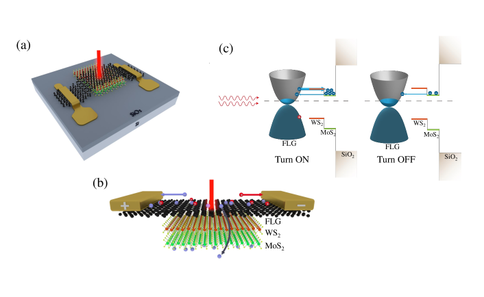
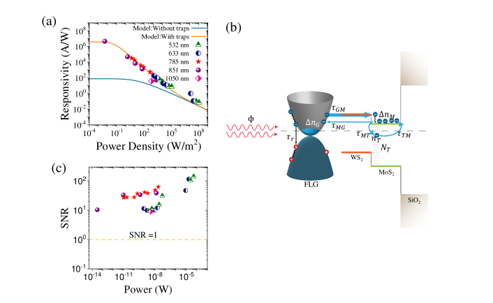
The architecture and working principle of the proposed device is explained schematically in Fig. 1a-c. The vertical stack consists of a monolayer (1L) or bilayer (2L) WS2 film sandwiched between few-layer graphene (FLG) on top and 1L-MoS2 at the bottom. The whole stack is placed on Si substrate coated with 285 nm thermally grown SiO2. MoS2 having a conduction band offset with WS2, as shown in Fig. 1c, creates an ultra-thin quantum well for electrons, with SiO2 on the other side. Under light illumination with photon energy less than the excitonic gap of MoS2 (and WS2), electron-hole pairs are generated only in the graphene layer. Since inter-layer carrier transfer process in vdW heterojunction is extremely fast ( sub-ps) 47, 48, 49, 50, a fraction of the photo-generated electrons are transferred to the MoS2 quantum well through the ultra-thin WS2 layer before recombination in graphene (Fig. 1b and left panel of Fig. 1c). Depending on the wavelength of excitation, both tunneling and over-the-WS2-barrier transfer processes are possible. The electrons, after being transferred to MoS2, swiftly thermalize to the conduction band edge of MoS2. A fraction of these carriers can also be captured by the sub-bandgap trap states 51 in MoS2. The trapped carriers in the MoS2 quantum well can in further tunnel through the WS2 barrier layer to come back to graphene. These population and depopulation mechanisms are quite fast due to the ultra-fast nature of the inter-layer charge transfer, which help to quickly create a steady state photoelectron population in the MoS2 floating quantum well. The WS2 spacer being an ultra-thin layer allows strong electrostatic coupling between the MoS2 layer and the graphene channel. The MoS2 quantum well with the captured photoelectrons thus acts as a floating gate on the graphene channel, modulating the Dirac point and the in-plane conductivity of the FLG film, in turn generating a measurable change in the current as detected by the electrodes shown in Figs. 1a-b.
Note that there is a strong built-in field due to the offset of the conduction band edges between MoS2 and graphene, as shown in the band diagram in Fig. 1c. Such field favors a fast inter-layer transfer of the stored photoelectrons in MoS2 to graphene. When the light source is turned off (Fig. 1c, right panel), the captured photoelectrons in the MoS2 quantum well thus swiftly tunnel through the WS2 barrier layer to graphene, and thus switching off the gating action immediately. This mechanism allows us to completely suppress the reminiscent photocurrent. Further, we do not need an external gate pulse to flush the confined photoelectrons. The detector thus is expected to exhibit a fast response due to the intrinsically small time scale of the inter-layer charge transfer and the high in-plane carrier mobility in graphene.
2.2 Evidence of carrier storage in MoS2 floating quantum well
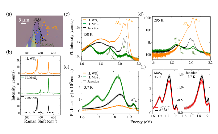
Fig. 2a shows the optical image of a fabricated FLG/1L-WS2/1L-MoS2 stack, along with isolated 1L-WS2 and 1L-MoS2 portions as controls. The Raman shifts from the isolated portions, as well as from the junction are shown in Fig. 2b. Under illumination, to demonstrate the charge storage in the bottom monolayer MoS2 without immediately being transferred to graphene through WS2, we employ photoluminescence (PL) quenching measurement. Figs. 2c-d show the PL intensity acquired from the isolated 1L-WS2 (in orange), isolated 1L-MoS2 (in green) and the junction (in black) separately at 150 K and 295 K with 532 nm laser excitation. At 150 K the monolayer WS2 shows the exciton () peak around 2.07 eV and the trion () peak around 2.04 eV, whereas the monolayer MoS2 exhibits the peak around 1.94 eV, and the peak at around 1.90 eV. On the junction, although there is no significant change in the peak position in the PL spectra (due to a combined effect of bandgap renormalization and exciton binding energy reduction 52, 53), the WS2 PL shows almost 90% to 95% quenching of the exciton and the trion peaks. This indicates an ultra-fast inter-layer charge transfer from WS2 to both graphene and MoS2 before the radiative decay of the exciton. On the contrary, the MoS2 peaks do not show any significant quenching in the PL spectra at the junction. At 295 K, the peaks are red shifted due to a reduction in bandgap, but the observations regarding quenching remain similar to that at 150 K.
Further, to avoid any possible compensation effect by photo-carrier injection from WS2 to MoS2, we reduce the temperature to 3.7 K, thus pushing up the excitonic gap of 1L-WS2 to 2.1 eV, and selectively excite only the 1L-MoS2 layer at the junction with 633 nm laser as the photon energy ( 1.96 eV) is lower than the 1L-WS2 optical bandgap. The results as shown in Fig. 2e suggest that PL intensity of the trion peak (the exciton peak being truncated by the edge filter due to resonant excitation) of MoS2 is similar in isolated portion and at the junction. This unambiguously shows that it is possible to create a steady state population of stored photo-carriers in the MoS2 quantum well without being immediately transferred to graphene - allowing for the proposed photogating action. To confirm the point further, we also perform circular polarization resolved PL experiment using near resonant excitation in MoS2 by 633 nm laser at 3.7 K (Fig. 2f). We obtain a similar degree ( 25%, obtained by peak fitting with Voigt function) of circular polarization for the trion peak both on the isolated MoS2 (left panel) and on the junction (right panel), which indicates that the valley polarization of MoS2 trions remains intact at the junction. This further justifies suppression of additional scattering channel in MoS2 at the junction owing to desirable carrier confinement. Note that, at low temperature, we observe strong sub-bandgap luminescence both from WS2 and MoS2, indicating presence of defect states 54, 55, 56, 57, which play an important role in obtaining large photodetector gain, as explained later.
2.3 Photodetector fabrication and characterization
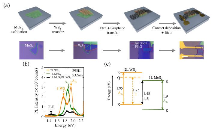
The photodetector (D1) fabrication process steps are illustrated in Fig. 3a. The device fabrication process starts with mechanical exfoliation of MoS2 flakes over Si substrate coated with 285 nm SiO2. 1L-MoS2 flakes are identified by optical contrast and Raman spectroscopy. The 2L-WS2 flake is then transferred on top of the 1L-MoS2 flake using a micromanipulator under optical microscope. For making MoS2 island, we use electron beam lithography, followed by dry etch using chlorine chemistry. FLG flake is then transferred on the heterostructure. Electrodes for contacting the FLG film are then defined by a second electron beam lithography step, followed by the deposition of Ni (10nm)/ Au (50nm) electrodes by DC sputtering and subsequent lift-off. A third lithography step followed by a final etch step is used to form a regular pattern of the FLG film so that graphene falls only on top of the WS2/MoS2 junction area, avoiding any un-gated parallel conduction path. More details on the layer transfer and device fabrication are provided in the Methods section. The junction area of the fabricated device is m2.
To demonstrate the concept proposed, we choose few-layer graphene over monolayer as the active layer. While monolayer graphene exhibits more gate tunability over few-layer, the choice of few-layer is to (1) enhance light absorption, (2) suppress substrate trap induced noise, and (3) reduce ambience induced detrimental effects. We also choose 2L-WS2 over 1L as the sandwiched barrier layer (1) to improve over-the-barrier injection from graphene to MoS2 due to suppressed barrier height, and (2) to increase the tunnelling width for band edge electrons in MoS2 to move back to graphene, thereby increasing the steady state population of captured photoelectron density in MoS2 floating gate. Fig. 3b shows the PL spectra of 1L-MoS2/2L-WS2 stack at 295 K, and the band-offset between the two can be inferred from the different peaks, as illustrated in Fig. 3c. The free exciton peaks of MoS2 (A and B) and WS2 (A) are distinctly observed from the isolated portions. The 2L-WS2 also clearly shows the indirect peak around 1.75 eV, indicating its bilayer nature. At the junction area, the exciton and indirect peaks of WS2 are quenched whereas the MoS2 peaks are distinctly discernable. We also observe a distinct inter-layer exciton peak at 1.45 eV, which is absent in the individual layers, indicating strong electronic coupling between the vdW layers.
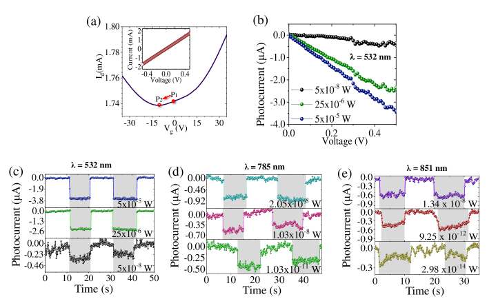
The - characteristics of the FLG under dark condition is shown in Fig. 4a, with a Dirac voltage () around V indicating n-type doping. We operate the device as a photodetector keeping the external gate voltage as zero. The operating point under dark condition is indicated by point . Under illumination, the captured photoelectrons by the MoS2 quantum well electrostatically gates the FLG, pushing the device operating point towards left to , providing a negative photocurrent, as schematically depicted in Fig. 1c. The top inset of Fig. 4a shows the drain voltage () dependent dark current under zero gate bias.
Fig. 4b shows the measured photocurrent () of the photodetector D1 as a function of , for three different optical powers () incident on the junction, at 532 nm excitation wavelength. Figs. 4c-e show the transient response of the photodetector at 532 nm, 785 nm, and 851 nm, respectively, illustrating fast switching for the incident powers used. The measured rise and fall times are found to be 10 ms, and only limited by the resolution of the measurement equipment. We do not observe any reminiscent photocurrent in the transient characteristics, which are typically observed in high-gain detectors using photo-gating effect. As mentioned earlier, this is achieved by the inherent built-in field in the device in the vertical direction that swiftly pushes the captured photo-carriers to graphene channel when light is turned off. This eliminates the requirement for additional refreshing circuit to push the detector to its original state. Note that the noise level is higher for the 532 nm excitation, which limits the detection of low power optical signal, while the noise level for 785 nm and 851 nm excitation is much lower, even when the incident power is very low (bottom panels of Figs. 4d-e). 532 nm photons having energy higher than the excitonic bandgap of MoS2 (and WS2), can be directly absorbed by these layers. The photo-generated large hot carrier density in MoS2 can in turn directly interact with the trap states in SiO2 substrate, causing a large noise. On the other hand, when excitation energy is smaller than MoS2 excitonic gap (for example, 785 and 851 nm), only graphene absorbs the excitation, followed by photoelectron transfer to MoS2 quantum well. During this process, the hot photo-carriers lose their energy, which significantly suppresses the interaction with the substrate traps states, reducing the gain noise and allowing us to detect optical signal down to 30 fW.
Using the above argument, the ultra-low noise level exhibited by the photodetector at sub-bandgap excitation of MoS2 and WS2 helps us to rule out a direct absorption by the defect states in these materials. Further, absorption of the near-infrared wavelengths used in this work would require involvement of deep level trap states of MoS2 and WS2. De-trapping of photocarriers from such deep trap states would be very slow, and would result in a slow decay of the photocurrent. The fast transient response observed from the detector thus corroborates that the effect of direct sub-bandgap absorption in MoS2 and WS2 layers can be ignored in our work.
2.4 Performance evaluation, modeling, and benchmarking
The extracted responsivity () of the photodetector is plotted in Fig. 5a as a function of incident optical power density for different wavelengths of excitation at V. There are two remarkable observations from this plot. First, the magnitude of the responsivity, particularly at low power density, is extremely high, reaching A/W at the minimum power density applied. This is several orders of magnitude higher than that of any reported detector based on light absorption by graphene, as shown in Table 1. Second, the responsivity follows the same trend line irrespective of the wavelength of the incident light, in agreement with broadband light absorption by graphene.
In order to get insights into such high gain mechanism in the detector, we construct a unified model that captures the density dependent recombination time of photo-carriers in graphene () 19, 58, fast inter-layer transfer of photo-carriers from graphene to MoS2 floating gate () and vice versa (), and possible trapping () and de-trapping times () of the carriers 59, 60 in the MoS2 bandgap. The coupled differential equations that govern the photoinduced carrier densities in graphene () and MoS2 (), and the trapped carrier density in MoS2 () are given by
| (1) |
| (2) |
| (3) |
where is the trap state density in MoS2 per unit area, is internal quantum efficiency of few-layer graphene absorption, and is the photon flux. Under steady state condition, putting the left hand sides of equations (1)-(3) to zero, and realizing that there is no net flow of charge from graphene to MoS2, we analytically obtain , , and . The responsivity can then be calculated as
| (4) |
where is Plank constant, is absolute electron charge, is velocity of light, is the excitation wavelength, is the extracted transconductance from Fig. 4a at operating point , is device active area, and is back gate oxide capacitance. The orange curve is the simulated responsivity with fitting parameters , , and cm-2. In the same plot, we also show the calculated by turning off the trap states in the model, as denoted by the blue curve. At high incident optical power density, the traps in MoS2 play a less important role and photocurrent saturation is dominated by reduction in in graphene with increasing photon flux. At low incident optical power density, as and , the relatively slow de-trapping of carriers builds up larger electron density in the trap states than in the conduction band of the floating MoS2 gate and thus traps play a major role in photogating and help obtaining the large responsivity. The simulated results follow the experimentally obtained remarkably well over 11 orders of magnitude of incident optical power density. The minor deviation of the simulated results from the data at smaller wavelength and high optical power density is because the model does not take into account direct absorption in MoS2. The experimentally obtained is slightly lower from the model predicted trend line at longer wavelength and is likely due to reduced energy of hot electrons, which affects the injection efficiency from graphene to MoS2.
In order to estimate the sensitivity of the device, we first extract the root mean squared noise current () integrated up to a detection bandwidth of 1 Hz, that is with an averaging time of 0.5 s. The electrical signal-to-noise ratio () is then obtained as
| (5) |
and plotted in Fig. 5c as a function of incident power for different wavelengths. The smallest power incident on the junction during the experiment is 30 fW (@851 nm), and even at such a low power, we obtain an of . Both nm and nm excitations, which directly excite the MoS2 and WS2 layers at the junction, produce smaller compared to the larger wavelength excitations. This is attributed to an enhanced noise level due to stronger interaction with SiO2 traps. The noise equivalent power () is a figure of merit that is often used to characterize the sensitivity and hence the minimum detectable optical power incident on the photodetector. represents the minimum input power required to obtain unity . The (normalized to 1 Hz) 61 of the detector is then calculated as
| (6) |
Since we only reached , from Equation 6, we estimate that the of the photodetector is fW/. The detection limit, as defined by is shown in Fig. 5c by the dashed line. We have shown the performance of another fabricated FLG/2L-WS2/1L-MoS2 heterojunction photodetector (D2) in Supporting Information S1. D2 exhibits a maximum responsivity of A/W, and fW/ at an excitation wavelength of 851 nm.
We benchmark the performance of the photodetector with existing photodetectors using graphene as light absorption medium. We note from the table that the detectors exhibiting high speed of operation suffers from low responsivity, while devices with larger gain show slow response. In this regard, the detector reported in this work not only outperforms any existing graphene-absorption based detector in terms of responsivity by several orders of magnitude, it also simultaneously achieves an extremely low and a fast response.
| Device description | Absorbing medium | R (A/W) | NEP (W/) | Response time (s) |
|---|---|---|---|---|
| FLG/WS2/MoS2 (This work) | Graphene | |||
| Metal/G/Metal detector 20 | Graphene | - | ||
| Suspended graphene 23 | Graphene | - | - | |
| Graphene with THz antenna 24 | Graphene | - | ||
| G/Ta2O5/G 30 | Graphene | |||
| G/MoS2 40 | Graphene | - | ||
| Metal/G/Metal with GQD arrays 45 | Graphene | - | ||
| Plasmonically enhanced graphene 62 | Graphene | - | ||
| Biased Graphene 63 | Graphene | - | - |
3 Conclusion
In summary, we have proposed and experimentally demonstrated a new class of highly sensitive photodetector that utilizes graphene as both light absorption medium as well as conduction channel and exploits ultra-fast inter-layer charge transfer to a floating quantum well enabling strong photogating. Graphene being the light absorbing medium, the photodetection principle is appealing for operation over a large wavelength range. The uniqueness of the device is demonstrated by eliminating the weak sensitivity observed in typical graphene-absorption based detectors. The proposed device achieves significantly superior performance over existing graphene-absorption-based photodetector reports in terms of simultaneously maintaining ultra-high responsivity, high signal to noise ratio at ultra-low incident power, and fast transient response, while reducing system level complexity by automatic flushing of captured photo-carriers when illumination is turned off. The photodetector also holds a key advantage in terms of maintaining room temperature operation, and using low-cost, less hazardous materials. The findings are appealing for highly sensitive broadband photodetection applications.
4 Methods
Device fabrication: The photodetector fabrication process steps are illustrated in Fig. 3a. The device fabrication process starts with mechanical exfoliation of MoS2 flakes over Si substrate coated with 285 nm SiO2. 1L-MoS2 flakes are identified by optical contrast and Raman spectroscopy. We then exfoliate WS2 flakes on PDMS sheet and identify 2L-WS2 using optical contrast and confirm with Raman and PL signal. The 2L-WS2 flake is then transferred on top of the 1L-MoS2 flake using a micromanipulator under optical microscope. For better adhesion, we heat this stack at 75∘C for 2 minutes on a hot plate. For making MoS2 island, we use electron beam lithography, followed by dry etch using chlorine chemistry. FLG flake is then transferred on the heterostructure using a similar technique discussed above, followed by another heating step. Electrodes for contacting the FLG film are then defined by a second electron beam lithography step, followed by the deposition of Ni (10nm)/ Au (50nm) electrodes by DC sputtering and subsequent lift-off. A third lithography step followed by a final etch step is used to form a regular pattern of the FLG film so that graphene falls only on top of the WS2/MoS2 junction area, avoiding any un-gated parallel conduction path.
This work was supported in part by a grant under Indian Space Research Organization (ISRO), by the grants under Ramanujan Fellowship, Early Career Award, and Nano Mission from the Department of Science and Technology (DST), and by a grant from MHRD, MeitY and DST Nano Mission through NNetRA.
Supporting Information is available on characterization of photodetector D2.
References
- Tan and Mohseni 2018 Tan, C. L.; Mohseni, H. Emerging Technologies for High Performance Infrared Detectors. Nanophotonics 2018, 7, 169–197
- Martyniuk et al. 2014 Martyniuk, P.; Antoszewski, J.; Martyniuk, M.; Faraone, L.; Rogalski, A. New Concepts in Infrared Photodetector Designs. Applied Physics Reviews 2014, 1, 041102
- Downs and Vandervelde 2013 Downs, C.; Vandervelde, T. E. Progress in Infrared Photodetectors Since 2000. Sensors 2013, 13, 5054–5098
- Potter and Eisenman 1962 Potter, R. F.; Eisenman, W. L. Infrared Photodetectors: A Review of Operational Detectors. Applied Optics 1962, 1, 567–574
- Rogalski 2011 Rogalski, A. Recent Progress in Infrared Detector Technologies. Infrared Physics and Technology 2011, 54, 136–154
- Craig et al. 2015 Craig, A. P.; Thompson, M. D.; Tian, Z. B.; Krishna, S.; Krier, A.; Marshall, A. R. InAsSb-Based nBn Photodetectors: Lattice Mismatched Growth on GaAs and Low-Frequency Noise Performance. Semiconductor Science and Technology 2015, 30, 105011(7pp)
- Gu et al. 2015 Gu, Y.; Zhou, L.; Zhang, Y.; Chen, X.; Ma, Y.; Xi, S.; Li, H. Dark Current Suppression in Metamorphic In0.83Ga0.17As Photodetectors with In0.66Ga0.34As/InAs Superlattice Electron Barrier. Applied Physics Express 2015, 8, 022202
- De Iacovo et al. 2016 De Iacovo, A.; Venettacci, C.; Colace, L.; Scopa, L.; Foglia, S. PbS Colloidal Quantum Dot Photodetectors Operating in the Near Infrared. Scientific Reports 2016, 6, 37913
- Cui et al. 2006 Cui, D.; Xu, J.; Xu, S. Y.; Paradee, G.; Lewis, B. A.; Gerhold, M. D. Infrared Photodiode Based on Colloidal PbSe Nanocrystal Quantum Dots. IEEE Transactions on Nanotechnology 2006, 5, 362–367
- Hall et al. 2004 Hall, D. J.; Buckle, L.; Gordon, N. T.; Giess, J.; Hails, J. E.; Cairns, J. W.; Lawrence, R. M.; Graham, A.; Hall, R. S.; Maltby, C.; Ashley, T. High-Performance Long-Wavelength HgCdTe Infrared Detectors Grown on Silicon Substrates. Applied Physics Letters 2004, 85, 2113–2115
- Lei et al. 2015 Lei, W.; Antoszewski, J.; Faraone, L. Progress, Challenges, and Opportunities for HgCdTe Infrared Materials and Detectors. Applied Physics Reviews 2015, 2, 041303
- Mak et al. 2012 Mak, K. F.; Ju, L.; Wang, F.; Heinz, T. F. Optical Spectroscopy of Graphene: From the Far Infrared to the Ultraviolet. Solid State Communications 2012, 152, 1341–1349
- Xia et al. 2009 Xia, F.; Mueller, T.; Lin, Y. M.; Valdes-Garcia, A.; Avouris, P. Ultrafast Graphene Photodetector. Nature Nanotechnology 2009, 4, 839–843
- Park and Ruiz-vargas 2009 Park, J.; Ruiz-vargas, C. Imaging of Photocurrent Generation and Collection in Single-Layer Graphene 2009. Nano Letters 2009, 9, 1742–1746
- Gabor et al. 2011 Gabor, N. M.; Song, J. C. W.; Ma, Q.; Nair, N. L.; Taychatanapat, T.; Watanabe, K.; Taniguchi, T.; Levitov, L. S.; Jarillo-Herrero, P. Hot Carrier–Assisted Intrinsic Photoresponse in Graphene. Science 2011, 334, 648–653
- Furchi et al. 2012 Furchi, M.; Urich, A.; Pospischil, A.; Lilley, G.; Unterrainer, K.; Detz, H.; Klang, P.; Andrews, A. M.; Schrenk, W.; Strasser, G.; Mueller, T. Microcavity-Integrated Graphene Photodetector. Nano Letters 2012, 12, 2773–2777
- Nair et al. 2008 Nair, R. R.; Blake, P.; Grigorenko, A. N.; Novoselov, K. S.; Booth, T.; Stauber, T.; Peres, N.; Geim, A. K. Fine Structure Constant Defines Visual Transparency of Graphene. Science 2008, 320, 1308
- George et al. 2008 George, P.; Strait, J.; Dawlaty, J.; Shivaraman, S.; Chandrashekhar, M.; Rana, F.; Spencer, M. G. Ultrafast Optical-Pump Terahertz-Probe Spectroscopy of the Carrier Relaxation and Recombination Dynamics in Epitaxial Graphene. Nano Lett 2008, 8, 4248–4251
- Rana et al. 2009 Rana, F.; George, P. A.; Strait, J. H.; Dawlaty, J.; Shivaraman, S.; Chandrashekhar, M.; Spencer, M. G. Carrier Recombination and Generation Rates for Intravalley and Intervalley Phonon Scattering in Graphene. Physical Review B 2009, 79, 115447
- Mueller et al. 2010 Mueller, T.; Xia, F.; Avouris, P. Graphene Photodetectors for High-Speed Optical Communications. Nature Photonics 2010, 4, 297–301
- Yoo et al. 2018 Yoo, T. J.; Kim, Y. J.; Lee, S. K.; Kang, C. G.; Chang, K. E.; Hwang, H. J.; Revannath, N.; Lee, B. H. Zero-Bias Operation of CVD Graphene Photodetector with Asymmetric Metal Contacts. ACS Photonics 2018, 5, 365–370
- Sassi et al. 2017 Sassi, U.; Parret, R.; Nanot, S.; Bruna, M.; Borini, S.; De Fazio, D.; Zhao, Z.; Lidorikis, E.; Koppens, F. H.; Ferrari, A. C.; Colli, A. Graphene-Based Mid-Infrared Room-Temperature Pyroelectric Bolometers with Ultrahigh Temperature Coefficient of Resistance. Nature Communications 2017, 8, 1–10
- Freitag et al. 2013 Freitag, M.; Low, T.; Avouris, P. Increased Responsivity of Suspended Graphene Photodetectors. Nano Letters 2013, 13, 1644–1648
- Spirito et al. 2014 Spirito, D.; Coquillat, D.; De Bonis, S. L.; Lombardo, A.; Bruna, M.; Ferrari, A. C.; Pellegrini, V.; Tredicucci, A.; Knap, W.; Vitiello, M. S. High Performance Bilayer-Graphene Terahertz Detectors. Applied Physics Letters 2014, 104, 061111
- Chen et al. 2015 Chen, Z.; Cheng, Z.; Wang, J.; Wan, X.; Shu, C.; Tsang, H. K.; Ho, H. P.; Xu, J. B. High Responsivity, Broadband, and Fast Graphene/Silicon Photodetector in Photoconductor Mode. Advanced Optical Materials 2015, 3, 1207–1214
- Chang et al. 2018 Chang, K. E.; Yoo, T. J.; Kim, C.; Kim, Y. J.; Lee, S. K.; Kim, S. Y.; Heo, S.; Kwon, M. G.; Lee, B. H. Gate-Controlled Graphene–Silicon Schottky Junction Photodetector. Small 2018, 14, 1801182
- Yu et al. 2013 Yu, W. J.; Liu, Y.; Zhou, H.; Yin, A.; Li, Z.; Huang, Y.; Duan, X. Highly Efficient Gate-Tunable Photocurrent Generation in Vertical Heterostructures of Layered Materials. Nature Nanotechnology 2013, 8, 952–958
- Wan et al. 2017 Wan, X. et al. A Self-Powered High-Performance Graphene/Silicon Ultraviolet Photodetector with Ultra-Shallow Junction: Breaking the Limit of Silicon? npj 2D Materials and Applications 2017, 1, 4
- Tao et al. 2017 Tao, L.; Chen, Z.; Li, X.; Yan, K.; Xu, J.-B. Hybrid Graphene Tunneling Photoconductor with Interface Engineering Towards Fast Photoresponse and High Responsivity. npj 2D Materials and Applications 2017, 1, 19
- Liu et al. 2014 Liu, C. H.; Chang, Y. C.; Norris, T. B.; Zhong, Z. Graphene Photodetectors with Ultra-Broadband and High Responsivity at Room Temperature. Nature Nanotechnology 2014, 9, 273–278
- Konstantatos et al. 2012 Konstantatos, G.; Badioli, M.; Gaudreau, L.; Osmond, J.; Bernechea, M.; De Arquer, F. P. G.; Gatti, F.; Koppens, F. H. Hybrid Graphene-Quantum Dot Phototransistors with Ultrahigh Gain. Nature Nanotechnology 2012, 7, 363–368
- Roy et al. 2013 Roy, K.; Padmanabhan, M.; Goswami, S.; Sai, T. P.; Ramalingam, G.; Raghavan, S.; Ghosh, A. Graphene-MoS2 Hybrid Structures for Multifunctional Photoresponsive Memory Devices. Nature nanotechnology 2013, 8, 826–830
- Yu et al. 2017 Yu, W.; Li, S.; Zhang, Y.; Ma, W.; Sun, T.; Yuan, J.; Fu, K.; Bao, Q. Near-Infrared Photodetectors Based on MoTe2/Graphene Heterostructure with High Responsivity and Flexibility. Small 2017, 13, 1700268
- Lan et al. 2017 Lan, C.; Li, C.; Wang, S.; He, T.; Zhou, Z.; Wei, D. Highly Responsive and Broadband Photodetectors Based on WS2-Graphene Van der Waals Epitaxial Heterostructures. Journal of Materials Chemistry C 2017, 5, 1494–1500
- Wu et al. 2018 Wu, J.-y.; Chun, Y. T.; Li, S.; Zhang, T.; Wang, J. Broadband MoS2 Field-Effect Phototransistors : Ultrasensitive Visible-Light Photoresponse and Negative Infrared Photoresponse. Advanced Materials 2018,
- Xiong et al. 2019 Xiong, Y.-f.; Chen, J.-h.; Lu, Y.-q.; Xu, F. Broadband Optical-Fiber-Compatible Photodetector with a Synergetic Photogenerating Mechanism. Advanced Electronic Materials 2019,
- Huo et al. 2017 Huo, N.; Gupta, S.; Konstantatos, G. MoS2–HgTe Quantum Dot Hybrid Photodetectors beyond 2 µm. Advanced Materials 2017, 29, 1606576
- Casalino et al. 2018 Casalino, M.; Russo, R.; Russo, C.; Ciajolo, A.; Gennaro, E. D.; Iodice, M.; Coppola, G. Free-Space Schottky Graphene/Silicon Photodetectors Operating at 2 m. ACS Photonics 2018, 5, 4577–4585
- Zhang et al. 2015 Zhang, W.; Chuu, C. P.; Huang, J. K.; Chen, C. H.; Tsai, M. L.; Chang, Y. H.; Liang, C. T.; Chen, Y. Z.; Chueh, Y. L.; He, J. H.; Chou, M. Y.; Li, L. J. Ultrahigh-Gain Photodetectors Based on Atomically Thin Graphene-MoS2 Heterostructures. Scientific Reports 2015, 4, 3826
- Vabbina et al. 2015 Vabbina, P.; Choudhary, N.; Chowdhury, A. A.; Sinha, R.; Karabiyik, M.; Das, S.; Choi, W.; Pala, N. Highly Sensitive Wide Bandwidth Photodetector Based on Internal Photoemission in CVD Grown p-Type MoS2/Graphene Schottky Junction. ACS Applied Materials and Interfaces 2015, 7, 15206–15213
- Sun et al. 2012 Sun, Z.; Liu, Z.; Li, J.; Tai, G. A.; Lau, S. P.; Yan, F. Infrared Photodetectors Based on CVD-Grown Graphene and PbS Quantum Dots with Ultrahigh Responsivity. Advanced Materials 2012, 24, 5878–5883
- Pan et al. 2018 Pan, R.; Li, H.; Wang, J.; Jin, X.; Li, Q.; Wu, Z.; Gou, J.; Jiang, Y.; Song, Y. High-Responsivity Photodetectors Based on Formamidinium Lead Halide Perovskite Quantum Dot-Graphene Hybrid. Particle and Particle Systems Characterization 2018, 35, 1700304
- Chang et al. 2017 Chang, P. H.; Liu, S. Y.; Lan, Y. B.; Tsai, Y. C.; You, X. Q.; Li, C. S.; Huang, K. Y.; Chou, A. S.; Cheng, T. C.; Wang, J. K.; Wu, C. I. Ultrahigh Responsivity and Detectivity Graphene-Perovskite Hybrid Phototransistors by Sequential Vapor Deposition. Scientific Reports 2017, 7, 46281
- Li et al. 2017 Li, J.; Yuan, S.; Tang, G.; Li, G.; Liu, D.; Li, J.; Hu, X.; Liu, Y.; Li, J.; Yang, Z.; Liu, S. F.; Liu, Z.; Gao, F.; Yan, F. High-Performance, Self-Powered Photodetectors Based on Perovskite and Graphene. ACS Applied Materials and Interfaces 2017, 9, 42779–42787
- Zhang et al. 2013 Zhang, B. Y.; Liu, T.; Meng, B.; Li, X.; Liang, G.; Hu, X.; Wang, Q. J. Broadband High Photoresponse from Pure Monolayer Graphene Photodetector. Nature Communications 2013, 4, 1811
- Tan et al. 2019 Tan, H.; Xu, W.; Sheng, Y.; Lau, C. S.; Fan, Y.; Chen, Q.; Tweedie, M.; Wang, X.; Zhou, Y.; Warner, J. H. Lateral Graphene-Contacted Vertically Stacked WS2/MoS2 Hybrid Photodetectors with Large Gain. Advanced Materials 2019, 1702917, 1–8
- Massicotte et al. 2016 Massicotte, M.; Schmidt, P.; Vialla, F.; Schädler, K. G.; Reserbat-Plantey, A.; Watanabe, K.; Taniguchi, T.; Tielrooij, K. J.; Koppens, F. H. Picosecond Photoresponse in Van der Waals Heterostructures. Nature Nanotechnology 2016, 11, 42–46
- Hong et al. 2014 Hong, X.; Kim, J.; Shi, S.-F.; Zhang, Y.; Jin, C.; Sun, Y.; Tongay, S.; Wu, J.; Zhang, Y.; Wang, F. Ultrafast Charge Transfer in Atomically Thin MoS2/WS2 Heterostructures. Nature Nanotechnology 2014, 9, 682–686
- Chen et al. 2016 Chen, H.; Wen, X.; Zhang, J.; Wu, T.; Gong, Y.; Zhang, X.; Yuan, J.; Yi, C.; Lou, J.; Ajayan, P. M.; Zhuang, W.; Zhang, G.; Zheng, J. Ultrafast Formation of Interlayer Hot Excitons in Atomically Thin MoS2/WS2 Heterostructures. Nature Communications 2016, 7, 12512
- Hill et al. 2017 Hill, M.; F., R. A.; Raja, A.; Chernikov, A.; Roquelet, C.; Heinz, T. F. Exciton Broadening in WS2 Graphene Heterostructures. Physical Review B 2017, 96, 205401
- Nan et al. 2014 Nan, H.; Wang, Z.; Wang, W.; Liang, Z.; Lu, Y.; Chen, Q.; He, D.; Tan, P.; Miao, F.; Wang, X.; Wang, J.; Ni, Z. Strong Photoluminescence Enhancement of MoS2 through Defect Engineering and Oxygen Bonding. ACS Nano 2014, 8, 5738–5745
- Ugeda et al. 2014 Ugeda, M. M.; Bradley, A. J.; Shi, S.-F.; da Jornada, F. H.; Zhang, Y.; Qiu, D. Y.; Ruan, W.; Mo, S.-K.; Hussain, Z.; Shen, Z.-X.; Wang, F.; Louie, S. G.; Crommie, M. F. Giant Bandgap Renormalization and Excitonic Effects in a Monolayer Transition Metal Dichalcogenide Semiconductor. Nature Materials 2014, 13, 1091–1095
- Gupta et al. 2017 Gupta, G.; Kallatt, S.; Majumdar, K. Direct Observation of Giant Binding Energy Modulation of Exciton Complexes in Monolayer MoSe2. Physical Review B 2017, 96, 081403
- Koperski et al. 2017 Koperski, M.; Molas, M. R.; Arora, A.; Nogajewski, K.; Slobodeniuk, A. O.; Faugeras, C.; Potemski, M. Optical Properties of Atomically Thin Transition Metal Dichalcogenides: Observations and Puzzles. Nanophotonics 2017, 6, 1289–1308
- Plechinger et al. 2016 Plechinger, G.; Nagler, P.; Arora, A.; Schmidt, R.; Chernikov, A.; del Águila, A. G.; Christianen, P. C.; Bratschitsch, R.; Schüller, C.; Korn, T. Trion Fine Structure and Coupled Spin–Valley Dynamics in Monolayer Tungsten Disulfide. Nature Communications 2016, 7, 12715
- Nagler et al. 2018 Nagler, P.; Ballottin, M. V.; Mitioglu, A. A.; Durnev, M. V.; Taniguchi, T.; Watanabe, K.; Chernikov, A.; Schüller, C.; Glazov, M. M.; Christianen, P. C. M.; Korn, T. Zeeman Splitting and Inverted Polarization of Biexciton Emission in Monolayer WS2. Physical Review Letters 2018, 121, 057402
- Vaclavkova et al. 2018 Vaclavkova, D.; Wyzula, J.; Nogajewski, K.; Bartos, M.; Slobodeniuk, A. O.; Faugeras, C.; Potemski, M.; Molas, M. R. Singlet and Triplet Trions in WS2 Monolayer Encapsulated in Hexagonal Boron Nitride. Nanotechnology 2018, 29, 325705
- Rana 2007 Rana, F. Electron-Hole Generation and Recombination Rates for Coulomb Scattering in Graphene. Physical Review B 2007, 76, 155431
- Knobloch et al. 2018 Knobloch, T.; Rzepa, G.; Illarionov, Y. Y.; Waltl, M.; Schanovsky, F.; Stampfer, B.; Furchi, M. M.; Mueller, T.; Grasser, T. A Physical Model for the Hysteresis in MoS2 Transistors. IEEE Journal of the Electron Devices Society 2018, 6, 972–978
- Furchi et al. 2014 Furchi, M. M.; Polyushkin, D. K.; Pospischil, A.; Mueller, T. Mechanisms of Photoconductivity in Atomically Thin MoS2. Nano Letters 2014, 14, 6165–6170
- Mackowiak et al. 2007 Mackowiak, V.; Jens, P.; Ma, Y.; Gorges, A. https://www.thorlabs.com/images/TabImages/Noise_Equivalent_Power_White_Paper.pdfNEP – Noise Equivalent Power. 2007; \urlhttps://www.thorlabs.com/images/TabImages/Noise_Equivalent_Power_White_Paper.pdf
- Ma et al. 2018 Ma, P.; Salamin, Y.; Baeuerle, B.; Josten, A.; Heni, W. Plasmonically Enhanced Graphene Photodetector Featuring 100 GBd , High-Responsivity and Compact Size. ACS Photonics 2018,
- Freitag et al. 2013 Freitag, M.; Low, T.; Xia, F.; Avouris, P. Photoconductivity of Biased Graphene. Nature Photonics 2013, 7, 53–59
See pages 1-3 of SI