Light emission from the layered metal 2H-TaSe2 and its potential applications
Abstract
1 Introduction
Adding new functionalities to devices is one of the important achievements of nano-materials and their heterojunctions. To this end, semiconducting two-dimensional (2D) transition metal dichalcogenides (TMDCs) have been extensively investigated for a plethora of nanoelectronic and optoelectronic applications 1, 2, 3. In general, obtaining a low resistance electrical contact without destroying the high quality of ultra-thin 2D active layers remains an outstanding challenge for 2D materials. Recently, vertical electronic and optoelectronic devices 1, 4, 5, 6 using layered materials are becoming increasingly popular as they exploit carrier transport through these nanometer-thick active layers - something that is difficult to achieve in a lithography limited conventional planar structure. Maintaining the pristine nature of the layers underneath the contact becomes even more crucial in the context of these vertical devices where the contact physically sits right on top of the active layers.
In this context, metallic TMDCs would be an ideal choice for contact material. However, metallic TMDCs remain a less explored class of materials. 2H-TaSe2 is one such layered TMDC that shows metallic properties 7, 8, 9, 10 and would be promising as a contact material for nanoelectronic devices. 2H-TaSe2 exhibits simultaneously strong electron-phonon coupling and spin-orbit coupling 11, which play a crucial role in charge density wave (CDW) driven transport properties. It exhibits highest CDW transition temperature among TMDCs exhibiting 2H symmetry. The resulting bandstructure shows a narrow band around Fermi energy with uniquely structured Fermi surfaces. Interestingly, there is a large gap above and below the bands around the Fermi energy 12, 13, 14, 15 in the normal metal phase and is expected to exhibit interesting optical properties, which remain largely unexplored. The perfect combination of excellent electrical transport and optical properties, coupled with the possibility of wafer-scale growth 16, makes 2H-TaSe2 a unique material for flexible, “all-2D” optoelectronic applications.
Motivated by this, in this work, we explore 2H-TaSe2 as a promising multi-purpose optoelectronic material. We show that this material exhibits strong optical absorption and photoluminescence, while maintaining metallic conductivity behavior. These properties have been explored here to demonstrate versatile device applications of 2H-TaSe2, for example, (1) as a donor layer for non-radiative resonant energy transfer (NRET) 17, 18, 19, 20 to other material, (2) as an efficient hot electron injector, (3) as a contact material for planar and vertical devices, and finally (4) as a dual-purpose layer, namely as light absorber as well as photo-carrier collector, in a sensitive, high speed vertical photodetector.
2 Results
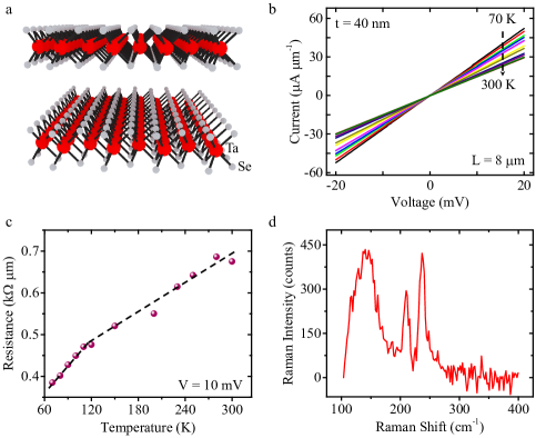
We obtain TaSe2 flakes on Si substrate covered with thermally grown nm SiO2 using micromechanical exfoliation from bulk crystals (procured from 2D Semiconductors). The bulk crystals are characterized using scanning electron micrograph (SEM), X-ray diffraction (XRD), and energy-dispersive X-ray spectroscopy (EDS) (see Supplementary Note 1). We use temperature dependent resistivity measurement and Raman spectroscopy to determine the polytype of the TaSe2 samples we use in this work. 1T-TaSe2 has an octahedral coordination and exhibits a normal metal to incommensurate, and incommensurate to commensurate CDW phase transition at K and K, respectively, with the latter being associated with a sharp discontinuity in resistivity 7, 21, 22. On the other hand, the 2H-TaSe2 polytype exhibits a trigonal prismatic structure (see Figure 1a) and remains normal metal above K. Upon cooling below K, it undergoes a CDW phase transition from metallic to incommensurate phase. On further cooling, it undergoes a first order lock in transition to commensurate ordered transition around K 11, 15. Unlike the 1T polytype, 2H-TaSe2 does not exhibit any discontinuity in resistivity. The current-voltage characteristics of a nm thick flake is shown in Figure 1b at different temperatures (). The normal metal to incommensurate CDW phase transition shows a sharp change in the slope in the resistivity (extracted from Figure 1b) versus plot 8, 9, 10, as shown in Figure 1c around K. Above this temperature, 2H-TaSe2 resistivity follows a functional form with and being constants, which is different from the law a conventional metal obeys. The term arises from impurity scattering due to local CDW fluctuation 9. Below the transition temperature , the resistivity drops as up to K, and as for K 9.
2H-TaSe2 also exhibits conspicuous Raman active A, E and E modes 10, 23, 24, as illustrated in Figure 1d. The A peak corresponds to the out of plane vibration mode at a wave number of cm-1, the E peak corresponds to in-plane vibrational mode at cm-1 and a broad E peak at cm-1 result from two-phonon processes. In Supplementary Note 2, we show the X-ray photoelectron spectrum of Ta core levels (4f5/2 and 4f7/2), both before and after an in-situ sputter etch step. The peak positions correlate well with TaSe2 25. Note that, in the pre-etch measurement, while we do not observe any distinct tantalum oxide peak, after curve fitting, a higher energy peak is found which shows presence of an ultra-thin surface oxide layer. This self-limiting layer acts as a protective layer to further oxidation. We provide a detailed short term and long term stability analysis of the TaSe2 flakes in Supplementary Note 3 using a combination of optical imaging, atomic force microscopy and Raman spectroscopy.
2.1 Photoluminescence from metallic TaSe2
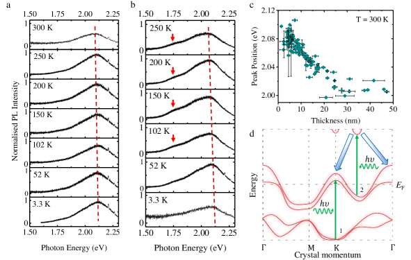
In spite of showing metal-like conductivity behavior, the 2H-TaSe2 flakes exhibit surprisingly strong photoluminescence (PL). We acquire PL spectra from TaSe2 flakes of varying thickness using continuous wave laser of wavelength nm at different temperatures from K to K where the sample chamber is kept at a high vacuum level of less than bar. The laser power is kept below W during the PL experiment. The obtained spectra from flakes of two different thickness values (monolayer and nm thick multi-layer) are shown in Figure 2a-b. Multiple features can be readily identified in the spectra: (1) Both the films exhibit a broad prominent peak around eV - eV. (2) No such strong luminescence is observed when an excitation with lower energy photon ( nm) is used. (3) The peak position blue shifts by about - meV depending on the thickness as the temperature is lowered from K to K. (4) Upon cooling below K, and further below K, the bands of 2H-TaSe2 are known to get significantly distorted to a “spaghetti-like” structure due to reconstruction 11. However, we do not observe any strong signature of such reconstruction in the photoluminescence. (5) For the thick film, a weak peak is identified around eV (indicated by red arrow in Fig 2b), particularly at higher temperature, and this is negligible in the monolayer. Figure 2c summarizes the thickness dependence of the peak position, measured over a large number of samples at K, suggesting a modulation of about meV can be achieved in the emission energy by changing the thickness of the flake. It is worth noting that photoluminescence has been reported in the past from films of tantalum based compounds which have been intentionally oxidized by exposing to relatively higher power laser beam 26, 27, 28. However, in our experiment, the origin of such strong PL from laser induced oxidation can be ruled out since the measurement is performed in high vacuum condition, and the laser power is also kept about an order of magnitude lower. In Supplementary Note 4, we provide a full spectrum of the PL showing the Raman lines close to the laser excitation, which suggests absence of any oxide Raman peak. Also, the strong dependence of the photoluminescence peak positions on the thickness of the TaSe2 films clearly suggests that the observed luminescence is not resulting from any surface-oxide layer. To further establish the point that any ambience induced surface oxidation (during exfoliation) does not give rise to the observed photoluminescence, we perform exfoliation followed by Poly(methyl methacrylate) (PMMA) spin coating inside a glovebox with N2 atmosphere. The coated samples exhibit similar photoluminescence and Raman characteristics, including a shift in the photoluminescence peak with change in flake thickness, as explained in Supplementary Note 5.
The general features of the light absorption and PL spectra can be qualitatively understood from the reported electronic structure of 2H-TaSe2, both using density functional calculations 12, 13, 24, 29, tight-binding calculations 11, 12, 30 and angle resolved photoemission spectroscopy (ARPES) measurements 12, 14, 15, 30, 31. With an excitation energy of eV, two possible direct optical transitions can be identified, as illustrated in the schematic bandstructure of a few-layer-thick 2H-TaSe2 (in the normal metal state, without any reconstruction) in Figure 2d. Like other layered CDW materials, 2H-TaSe2 has a narrow band around the Fermi energy across the Brillouin zone. There are also a set of bands below and above it which are well separated in energy. Transition 1 is a direct inter-band transition from the bottom band to the band above the Fermi energy at point. The photo-carriers (both electrons and holes) thus generated are scattered in the k-space in a very short time scale. This process is similar to gold and copper 32, and results in a weak luminescence. On the other hand, transition 2 (in between and ) causes a strong optical absorption due to the parallel nature of the band pair. The photo-generated electrons from the upper band relax to the and valley through indirect transitions with the assistance of phonons - resulting in luminescence.
The full width at half maximum (FWHM) of the peaks is - meV and is significantly larger compared with typical excitonic resonance observed in monolayers of semiconducting TMDCs (like MoS2, MoSe2, WS2, and WSe2). The linewidth remains large irrespective of the thickness and sample temperature, even down to K and can be understood from the indirect nature of carrier relaxation, as well as strong scattering from the free carriers. We also did not observe any sharp excitonic feature in differential reflectance spectra of the flakes, as shown in Supplementary Note 6.
In order to probe the lifetime of the photo-excited carriers in TaSe2, we perform time-resolved photoluminescence (TRPL) measurements. The measurement details and the results are summarized in Supplementary Note 7. Supplementary Figure 10d shows the statistical distribution of the lifetimes extracted after deconvolving the observed data with instrument response function (IRF) across all measurements (measured over seven different flakes, several spots on each flake). The dotted curves in Supplementary Figure 10d represent Gaussian fit to the distributions. The mean values of extracted lifetimes are 6.8 ps for 45 W and 2.5 ps for 140 W of incident power at 405 nm excitation wavelength. The distributions are found to be quite tight, with a standard deviation of 1.4 ps for 45 W and 0.9 ps for 140 W of excitation power. We, however, note that there may be some inaccuracy in these extracted lifetime values due to the closeness of the measured data with IRF. These lifetime values for the photo-carriers are significantly longer than, for example, what one would get in conventional metallic systems - a key result that is exploited later for efficient hot electron injection from TaSe2 to other semiconducting TMDC.
2.2 Resonant energy transfer between TaSe2 and MoS2
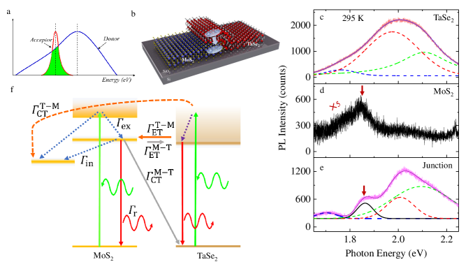
The broad emission linewidth from TaSe2 has a large spectral overlap with the excitonic absorption of other semiconducting TMDC materials like exciton of MoS2, as schematically shown in Figure 3a. We exploit this feature to transfer energy from TaSe2 to other semiconducting TMDC layers using dipole-dipole coupling through NRET process 17, 18, 19. Due to layered structure, the transition dipoles formed in both MoS2 and TaSe2 are quasi-two-dimensional in nature. The dipole-dipole interaction between these two vertically stacked materials is facilitated due to such in-plane orientation of the transition dipoles, which allow matching of the center of mass momentum 33, as schematically depicted in Figure 3b. We prepare multiple TaSe2 (top)/multi-layer MoS2 (bottom) vertical heterojunction stacks on Si/SiO2 substrate (see Methods). Figure 3c shows the PL spectrum from the part of the TaSe2 flake which is not on the junction. The data can be fitted with three different Voigt peaks, as shown by the dashed lines. We use a multi-layer MoS2 to ensure that the luminescence from the MoS2 flake alone is extremely weak. Figure 3d shows the weak MoS2 peak around eV which corresponds to the direct band gap transition at the point of the Brillouin zone. While plotting, the MoS2 peak intensity in multiplied by 5.
Figure 3e shows a seven-fold enhancement in the MoS2 PL intensity (indicated by the arrow) in the TaSe2/MoS2 junction. The resulting photoluminescence spectrum from the junction can now be fitted with four Voigt peaks, three from TaSe2 (in dashed traces) and the fourth one representing MoS2 emission (in solid black trace). At the junction, while the MoS2 peak is enhanced, the individual dashed traces clearly indicate the suppression of the strength of the TaSe2 emission at the emission energy of MoS2, justifying energy transfer from TaSe2 to exciton. The underlying mechanism is explained schematically in Figure 3f where the rates of the individual processes are indicated. In multi-layer MoS2, the direct peak is weak due to fast (on the order of fs 34) transfer of carriers to lower energy indirect valleys. The photo-excited carriers generated by an excitation with nm (i.e. eV) photon - that is off-resonant with the 1s peak - transfers to the lower valleys rather than forming an exciton in the and valleys.
According to the experimental data, photoluminescence of the MoS2 A peak gets enhanced at the MoS2/TaSe2 junction suggesting a gain channel for exciton density. MoS2 gains excitons at the () valley at a Forster NRET rate () from the energy states in TaSe2 that are resonant to the exciton state of MoS2. The MoS2 excitons decay through multiple parallel channels, namely the radiative recombination () and non-radiative processes including scattering to lower energy indirect valley in MoS2 (), as well as Dexter () and Forster () process induced exciton back transfer to TaSe2. With this understanding, we form the rate equations for exciton density in MoS2 () and free e-h pair density in TaSe2 () on junction, as explained in Supplementary Note 8.
The PL enhancement factor () is defined to be the ratio of the steady state PL intensity of MoS2 on TaSe2 to that of on SiO2 and turns out to be
| (1) |
where relevant variables are defined in Supplementary Note 8. Equation 1 suggests that the enhancement factor increases as decreases due to improved energy transfer with a maximum attainable value of . Such an efficient resonant energy transfer process is lucrative for a variety of optoelectronic applications, including electroluminescence 35.
2.3 TaSe2 as an efficient hot carrier injector
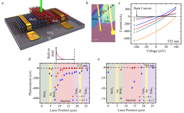
The strong light absorption by TaSe2 makes it a promising material for hot carrier injection to other semiconducting materials. We fabricate MoS2/TaSe2 heterojunction device with Ni/Au as contact pads, as schematically shown in Figure 4a (see Methods). A laser beam of wavelength nm is scanned from one contact to the other (along the arrow in the optical image in Figure 4b), and we measure the corresponding photocurrent (see Methods) at different external bias conditions. Figure 4c shows the current-voltage characteristics of the heterojunction for a few selected positions of the laser spot, as indicated by numbers. The dark current from the device is represented by the black line. The spatial dependence of the photocurrent is illustrated in Figure 4d at V by plotting the photocurrent as a function of the laser position.
When the laser spot is on the TaSe2 flake with no MoS2 underneath (points 5 and 6), we observe a strong photoresponse at a non-zero external bias. This strong photocurrent away from the junction is surprising when compared to other reported metal-TMDC junction devices 36. A weak photocurrent on the metal portion away from the junction has been attributed earlier to photo-thermoelectric effect due to laser spot induced local heating. However, in the present case, such a photo-thermoelectric effect can be ignored as the photocurrent strongly depends on the applied external bias, and is negligible under zero bias. This is further verified by noting that the photocurrent is extremely weak when a nm excitation is used (Figure 4e) which does not allow any inter-band transition in TaSe2. The strong photocurrent (with 532 nm) with the laser spot on TaSe2 suggests that the photo-electrons, generated by the inter-band transition in TaSe2, exhibit relatively longer recombination lifetime compared to other metals. This is in good agreement with the TRPL measurement discussed earlier. The long lifetime allows us to collect the photoelectrons at the contact even when the separation between the laser spot and the metal contact is several micrometers (for example, point 6 in Figure 4b), which is few orders of magnitude longer than conventional metals. This makes TaSe2 particularly attractive material as a source for efficient hot carrier injection techniques.
When the excitation wavelength is 532 nm, the device exhibits a large open circuit voltage () and short circuit current () which strongly depend on the position of the laser spot, as explained in Figure 4c. The asymmetry between Au/MoS2 and TaSe2/MoS2 junctions provides a strong built-in field in the device. is maximum when the laser spot is directly on the MoS2 channel, and this leads to a of V. and are zero on the other hand when the laser is on TaSe2 as there is no built-in field in TaSe2 owing to its high electrical conductivity. In between, upon moving the laser spot away from the MoS2 channel towards right along the arrow in Figure 4b, the and are gradually suppressed. Using transfer length theory 37, 38 of metal-semiconductor contacts, the built-in field dies rapidly in the lateral direction in the MoS2 portion underneath TaSe2 (see top panel of Figure 4d), resulting in a gradual suppression of the zero-bias photocurrent as the laser spot is moved away from the MoS2 channel.
2.4 Graphene/MoS2/TaSe2 vertical junction
Inspired by the strong built-in electric field in the lateral heterojunction device in Figure 4, we next fabricate a vertical heterojunction 2H-TaSe2/2H-MoS2/1L-graphene (see Methods), as schematically shown in Figure 5a. Two-dimensional layered materials have recently attracted a lot of attention as active material in photodetector applications 39, 40, 41. Vertical heterojunction photodetectors based on ultra-thin two-dimensional layered materials provide a number of advantages 5, 42 compared to lateral structures, namely (1) ultra-short carrier transit time due to nanometer separated electrodes, which is difficult to achieve otherwise in a lithography limited planar structure; (2) large built-in vertical field; (3) suppression of series resistance due to improved carrier collection efficiency that is not limited by transfer length; and (4) repeatable characteristics where encapsulated photoactive layer does not degrade from ambience effects and screened from substrate induced traps.
The difference in the work function between TaSe2 and monolayer (1L) graphene provides a strong built-in field across the few-layer MoS2 film which is sandwiched between the two. The structure utilizes the excellent electrical contact between TaSe2 and MoS2, while maintaining the pristine nature of MoS2 at the junction which is critical for the operation of such vertical heterojunction. Monolayer graphene at the bottom serves two purposes. First, it acts like the bottom electrode for carrier collection. Second, using the weak screening through graphene, a back-gate can be used to modulate the chemical potential of the MoS2 sandwiched layer.
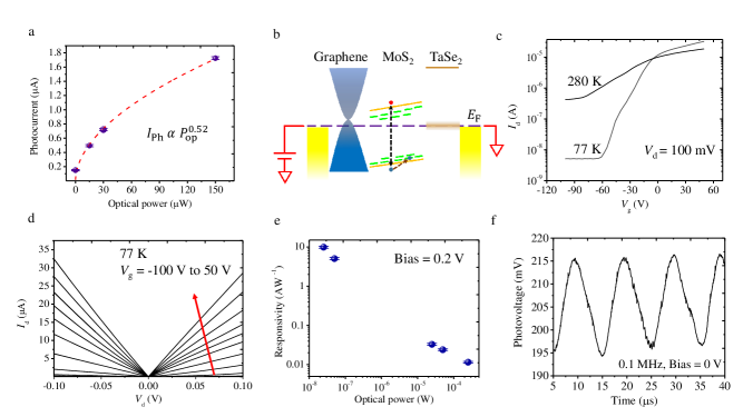
The optical image of the fabricated heterojunction device is shown in Figure 5b. The photocurrent () from the device is obtained as where is the measured current in presence of light and is the dark current. Figure 5c illustrates the variation of as a function of external bias when excited with a diffraction limited laser spot (diameter m) of wavelength nm. The vertical built-in field in the device manifests as a nonzero photocurrent at zero external bias. Three possible mechanisms that can contribute to the photocurrent are schematically depicted in Figure 5d-f. The left and right panels represent the state transition diagrams and the electronic band diagrams, respectively. The first process is explained in Figure 5d. NRET driven energy transfer due to dipole-dipole interaction between TaSe2 and MoS2 results in a creation of exciton in MoS2 due to light absorption in TaSe2. The exciton thus created in MoS2 is dissociated at a fast time scale due to scattering to lower energy indirect valleys, creating free electron and hole at the band edges. These electrons and holes are in turn separated by the built-in field, giving rise to photocurrent. Such an energy transfer driven photocurrent generation is a unique way of photodetection, and can find multiple applications in van der Waals heterojunctions. Second, the light absorbed by TaSe2 creates hot electrons, which are injected into MoS2. The built-in field in MoS2 carries these electrons towards graphene, resulting in photocurrent, as shown in Figure 5e. Third, the electron-hole pairs generated by the photons directly absorbed in MoS2 also result in population in the band edge indirect valleys, causing photocurrent, as explained in Figure 5f.
In order to segregate the effect of the above three mechanisms, the photocurrent is measured with nm excitation (which is not absorbed by TaSe2), and the current-voltage characteristics are summarized in the inset of Figure 5c. We notice that the photocurrent at zero external bias is completely suppressed. This indicates that the zero-bias photocurrent for nm excitation is primarily governed by TaSe2 induced hot carrier transfer and dipole-dipole interaction driven NRET process.
The photocurrent is plotted as a function of the incident optical power () of 532 nm excitation in Figure 6a. The data can be fitted with a power law: , which indicates that the traps due to the gap states in MoS2 play an important role in determining . The presence of gap states in MoS2 (see Figure 6b) is also identified by the back gate modulation of the electrical conductivity of the device. Figure 6c shows the transfer characteristics [drain current () versus gate voltage ()] where is applied at the back side. Upon cooling the device to 77 K, we obtain an on-off ratio of , which reduces to at K. The on-off ratio at K suffers from tunneling of carriers from bottom graphene electrode to top TaSe2 electrode though the bandgap states in MoS2 resulting from band tail states as well as deep traps due to defects 43. The tunneling effect manifests in a particularly strong manner for large negative , where the gate voltage dependence on the drain current is completely absent due to the tunneling leakage. When the device is cooled down to K, the trap assisted tunneling can be reduced significantly. The output characteristics [ versus drain voltage ()] of the vertical device at K are displayed in Figure 6d.
Figure 6e shows the obtained responsivity from the device at different incident optical powers. The responsivity is at the minimum power used, which suggests an internal gain in the device. The different photo-carrier generation mechanisms described earlier also populate the trap states closer to the valence band of MoS2 with holes. This in turn results in a gain mechanism 42, 43. Two possible mechanisms, namely photoconductive gain and photogating effect, provide gain in the system. Photo-generated holes trapped in the gap states of the MoS2 film cause a charge imbalance forcing reinjection of electrons multiple times before the trapped hole recombines or tunnels out of MoS2 - providing photoconductive gain. Electron trapping is neglected as the Fermi level in MoS2 lies close to the conduction band edge. Since the photoconductive gain is given by , where is the lifetime of the hole in the trap state, the vertical structure is advantageous due to its short transit time () of electrons through the thin MoS2 layer 5. On the other hand, the trapped holes suppress the barrier for carrier injection to MoS2 from vertical electrodes, providing a photogating effect.
The heterostructure device is further characterized for the speed of operation using a laser which is intensity modulated with varying frequency. The photovoltage generated by the device is measured across a digital storage oscilloscope which is terminated with M impedance. Figure 6f shows the measured photovoltage in response to a MHz modulation frequency under zero external bias operation, which is one of the fastest reported photodetectors using TMDC material. The short transit time of the photo-electrons helps to obtain the high speed of operation of the detector, while maintaining the gain. In Supplementary Table 1, we compare the performance of the photodetector presented in this work with existing 2D material based detectors (having response time less than 100 ms).
3 Discussion
In summary, we demonstrate the versatility of 2H-TaSe2 as a two-dimensional layered CDW material, which exhibits metal-like characteristics, coupled with strong light absorption and emission due to energy separated bands. The narrow band around the Fermi energy results in giant metallic conductivity with temperature dependent CDW characteristics. This makes TaSe2 an ideal candidate for a 2D-2D van der Waals contact material which can maintain the pristine nature of the underneath 2D layered semiconductor. On the other hand, the well separated bands lying above and below the Fermi energy result in strong inter-band optical absorption, strong photoluminescence and a long lifetime of photoelectrons generating large photocurrent. The spectral overlap between emission of TaSe2 and excitonic absorption of other TMDC semiconductors like MoS2 results in a unique in-plane momentum matched 2D-2D combination of donor-acceptor pair causing a giant enhancement of photoluminescence in multi-layer MoS2 due to non-radiative resonant energy transfer. TaSe2 is further utilized as a dual purpose layer in a vertical photodetection device to obtain high speed and gain simultaneously. The large separation of the bands also make TaSe2 an interesting material for low-loss plasmonic applications 44, 45. The finding will ignite multiple device applications using 2H-TaSe2 in the nano-opto-electronic domain.
4 Methods
4.1 Heterojunction device fabrication
For both planar and vertical devices, the 2D material stack is fabricated by using dry transfer technique on a highly doped Si substrate coated with nm thick thermally grown oxide. This stack is heated on a hot plate at C for 2 minutes for improved adhesion between layers. Devices are fabricated using standard nano-fabrication methods. The substrate is spin coated with PMMA C and baked on a hot plate at C for minutes. This is followed by electron beam lithography with an acceleration voltage of KV, an electron beam current of pA, and an electron beam dose of Ccm-2. Patterns were developed using MIBK:IPA solution in the ratio . Later samples are washed in isopropyl alcohol and dried in N2 blow. nm Ni / nm Au films are deposited by using magnetron sputtering with the help of Ar plasma at mBar. Metal lift-off was done by dipping the substrate in acetone for minutes, followed by washing in isopropyl alcohol and drying. The bottom side of the wafer is etched by dilute HF solution and silver film is deposited as the bottom gate contact.
4.2 Photocurrent measurements
Devices are probed by micromanipulators, connected to a Keithley 2636B and Agilent B1500 device analyzers for electrical measurements. Diffraction limited laser spots of wavelength 532 nm and 785 nm are used for photocurrent measurements through a 50 objective with a numerical aperture of 0.5. The device is kept on a motorized stage to obtain spatial mapping of photocurrent. For low temperature electrical measurements, a liquid nitrogen cooled stage is used. High speed measurements are performed using a 532 nm laser beam. The intensity of the laser beam is modulated at the required frequency, up to 0.1 MHz and the photovoltage measured using a digital storage oscilloscope which is terminated by 10 M.
Data availability
The datasets generated and analyzed during the current study are available from the corresponding author on reasonable request.
References
- 1 Lee, C.H et al. Atomically thin p–n junctions with van der waals heterointerfaces. Nature nanotechnology 9, 676 (2014).
- 2 Withers, F. et al. WSe2 light-emitting tunneling transistors with enhanced brightness at room temperature. Nano letters 15, 8223–8228 (2015).
- 3 Shim, J. et al. Electronic and optoelectronic devices based on two-dimensional materials: From fabrication to application. Advanced Electronic Materials 3, 1600364 (2017).
- 4 Massicotte, M. et al. Picosecond photoresponse in van der waals heterostructures. Nature nanotechnology 11, 42–46 (2016).
- 5 Kallatt, S., Nair, S. & Majumdar, K. Asymmetrically encapsulated vertical ITO/MoS2/Cu2O photodetector with ultrahigh sensitivity. Small 14, 1702066 (2018).
- 6 Withers, F. et al. Light-emitting diodes by band-structure engineering in van der waals heterostructures. Nature materials 14, 301 (2015).
- 7 Wilson, J.A., Di Salvo, F.J. & Mahajan, S. Charge-density waves in metallic, layered, transition-metal dichalcogenides. Physical review letters 32, 882 (1974).
- 8 Lee, H., Garcia, M., McKinzie, H. & Wold, A. The low-temperature electrical and magnetic properties of TaSe2 and NbSe2. Journal of Solid State Chemistry 1, 190–194 (1970).
- 9 Naito, M. & Tanaka, S. Electrical tranport properties in 2H-NbS2, -NbSe2, -TaS2 and -TaSe2. Journal of the Physical Society of Japan 51, 219–227 (1982).
- 10 Neal, A. T., Du, Y., Liu, H. & Ye, P. D. Two-dimensional TaSe2 metallic crystals: spin–orbit scattering length and breakdown current density. Acs Nano 8, 9137–9142 (2014).
- 11 Rossnagel, K. & Smith, N.V. Spin-orbit splitting, fermi surface topology, and charge-density-wave gapping in 2H-TaSe2. Physical Review B 76, 073102 (2007).
- 12 Laverock, J. et al. k-resolved susceptibility function of 2H-TaSe2 from angle-resolved photoemission. Physical Review B 88, 035108 (2013).
- 13 Renteria, J. et al. All-metallic electrically gated 2H-TaSe2 thin-film switches and logic circuits. Journal of Applied Physics 115, 034305 (2014).
- 14 Tsoutsou, D. et al. Epitaxial 2d MoSe2 (HfSe2) semiconductor/2D TaSe2 metal van der waals heterostructures. ACS applied materials & interfaces 8, 1836–1841 (2016).
- 15 Li, Y.W. et al. Folded superstructure and degeneracy-enhanced band gap in the weak-coupling charge density wave system 2H- TaSe2. Physical Review B 97, 115118 (2018).
- 16 Shi, J. et al. Chemical vapor deposition grown wafer-scale 2D Tantalum Diselenide with robust charge-density-wave order. Advanced Materials 30, 1804616 (2018).
- 17 Kozawa, D. et al. Evidence for fast interlayer energy transfer in MoSe2/WS2 heterostructures. Nano letters 16, 4087–4093 (2016).
- 18 Guzelturk, B. & Demir, H. V. Near-field energy transfer using nanoemitters for optoelectronics. Advanced Functional Materials 26, 8158–8177 (2016).
- 19 Deshmukh, R. et al. Long-range resonant energy transfer using optical topological transitions in metamaterials. ACS Photonics 5, 2737–2741 (2018).
- 20 Dandu, M. et al. Strong single-and two-photon luminescence enhancement by non-radiative energy transfer across layered heterostructure. ACS nano 13, 4795–4803 (2019).
- 21 Wilson, J.A., Di Salvo, F.J. & Mahajan, S. Charge-density waves and superlattices in the metallic layered transition metal dichalcogenides. Advances in Physics 24, 117–201 (1975).
- 22 Inada, R., Ōnuki, Y. & Tanuma, S. Hall effect of 1T-TaS2 and 1T-TaSe2. Physica B+ C 99, 188–192 (1980).
- 23 Hajiyev, P., Cong, C., Qiu, C. & Yu, T. Contrast and raman spectroscopy study of single-and few-layered charge density wave material: 2H-TaSe2. Scientific reports 3, 2593 (2013).
- 24 Yan, J. A., Cruz, M. A. D., Cook, B. & Varga, K. Structural, electronic and vibrational properties of few-layer 2H- and 1T-TaSe2. Scientific reports 5, 16646 (2015).
- 25 Luo, H. et al. Differences in chemical doping matter: Superconductivity in Ti1-xTaxSe2 but not in Ti1-xNbxSe2. Chemistry of Materials 28, 1927–1935 (2016).
- 26 Castellanos-Gomez, A. et al. Fast and reliable identification of atomically thin layers of TaSe2 crystals. Nano Research 6, 191–199 (2013).
- 27 Coronado, E., Forment-Aliaga, A., Navarro-Moratalla, E., Pinilla-Cienfuegos, E. & Castellanos-Gomez, A. Nanofabrication of TaS2 conducting layers nanopatterned with Ta2O5 insulating regions via AFM. Journal of Materials Chemistry C 1, 7692–7694 (2013).
- 28 Cartamil-Bueno, S. J. et al. High-quality-factor tantalum oxide nanomechanical resonators by laser oxidation of TaSe2. Nano Research 8, 2842–2849 (2015).
- 29 Kuchinskii, E.Z, Nekrasov, I.A & Sadovskii, M.V. Electronic structure of two-dimensional hexagonal diselenides: charge density waves and pseudogap behavior. Journal of Experimental and Theoretical Physics 114, 671–680 (2012).
- 30 Smith, N.V., Kevan, S.D & Di Salvo, F.J. Band structures of the layer compounds 1T-TaS2 and 2H-TaSe2 in the presence of commensurate charge-density waves. Journal of Physics C: Solid State Physics 18, 3175 (1985).
- 31 Jakovidis, G., Riley, J. D. & Leckey, R. C. G. Experimental bandstructure of 2H-TaSe2. Journal of Electron Spectroscopy and Related Phenomena 61, 19–26 (1992).
- 32 Mooradian, A. Photoluminescence of metals. Physical Review Letters 22, 185 (1969).
- 33 Lyo, S.K. Energy transfer of excitons between quantum wells separated by a wide barrier. Physical Review B - Condensed Matter and Materials Physics 62, 13641–13656 (2000).
- 34 Bertoni, R. et al. Generation and evolution of spin-, valley-, and layer-polarized excited carriers in inversion-symmetric WSe2. Physical review letters 117, 277201 (2016).
- 35 Puchert, R. P. et al. Spectral focusing of broadband silver electroluminescence in nanoscopic fret-leds. Nature nanotechnology 12, 637 (2017).
- 36 Hong, T. et al. Plasmonic hot electron induced photocurrent response at MoS2–metal junctions. ACS nano 9, 5357–5363 (2015).
- 37 Schroder, D. K. Semiconductor material and device characterization (Wiley-Interscience, Hoboken, New Jersey, 2006).
- 38 Majumdar, K. et al. STLM: A sidewall tlm structure for accurate extraction of ultralow specific contact resistivity. IEEE Electron Device Letters 34, 1082–1084 (2013).
- 39 Koppens, F.H.L et al. Photodetectors based on graphene, other two-dimensional materials and hybrid systems. Nature nanotechnology 9, 780 (2014).
- 40 Li, X. et al. Graphene and related two-dimensional materials: Structure-property relationships for electronics and optoelectronics. Applied Physics Reviews 4, 021306 (2017).
- 41 Mak, K. F. & Shan, J. Photonics and optoelectronics of 2D semiconductor transition metal dichalcogenides. Nature Photonics 10, 216 (2016).
- 42 Murali, K. & Majumdar, K. Self-Powered, Highly Sensitive, High-Speed Photodetection Using ITO/WSe2/SnSe2 Vertical Heterojunction. IEEE Transactions on Electron Devices 65, 4141–4148 (2018).
- 43 Furchi, M. M., Polyushkin, D. K., Pospischil, A. & Mueller, T. Mechanisms of photoconductivity in atomically thin MoS2. Nano letters 14, 6165–6170 (2014).
- 44 Khurgin, J. B. & Sun, G. In search of the elusive lossless metal. Applied Physics Letters 96, 181102 (2010).
- 45 Gjerding, M. N., Pandey, M. & Thygesen, K. S. Band structure engineered layered metals for low-loss plasmonics. Nature communications 8, 15133 (2017).
Acknowledgements
This work was partially supported in part by a grant under Indian Space Research Organization (ISRO), by the grants under Ramanujan Fellowship, Early Career Award, and Nano Mission from the Department of Science and Technology (DST), and by a grant from MHRD, MeitY and DST Nano Mission through NNetRA. S.G. acknowledges funding support from DST (SR/FST/ETII-072/2016) and SERB (SB/S2/RJN-134/2014, EMR/2016/007113).
Contributions
K.M. designed the experiment. M.M. and S.K. prepared the samples, fabricated the devices and performed the measurements. N.S. and S.G. performed the time-resolved photoluminescence measurement. M.D. contributed to the theoretical analysis of the energy transfer mechanism. All authors contributed to the data analysis, discussion of results, and writing of the paper. M.M. and S.K. contributed equally to this work.
Competing interests
The Authors declare no competing interests.
Corresponding author
Correspondence to K. Majumdar.

See pages 1-13 of Supplementary_Information