Influence of irradiation on defect spin coherence in silicon carbide
Abstract
Irradiation-induced lattice defects in silicon carbide (SiC) have already exceeded their previous reputation as purely performance-inhibiting. With their remarkable quantum properties, such as long room-temperature spin coherence and the possibility of downscaling to single-photon source level, they have proven to be promising candidates for a multitude of quantum information applications. One of the most crucial parameters of any quantum system is how long its quantum coherence can be preserved. By using the pulsed optically detected magnetic resonance (ODMR) technique, we investigate the spin-lattice relaxation time () and spin coherence time () of silicon vacancies in 4H-SiC created by neutron, electron and proton irradiation in a broad range of fluences. We also examine the effect of irradiation energy and sample annealing. We establish a robustness of the time against all types of irradiation and reveal a universal scaling of the time with the emitter density. Our results can be used to optimize the coherence properties of silicon vacancy qubits in SiC for specific tasks.
Introduction
Defect spins in silicon carbide (SiC) attract growing interest because of their high potential as multidimensional qubits – the so called qudits – for wafer-scale quantum information processing at room temperature Baranov et al. (2011); Koehl et al. (2011); Riedel et al. (2012); Weber et al. (2010). Particularly, silicon vacancies () and divacancies () demonstrate an extremely long spin-lattice relaxation time () and spin coherence time (), even in commercial wafers without isotope purification Falk et al. (2013); Yang et al. (2014); Carter et al. (2015); Seo et al. (2016); Simin et al. (2017); Fischer et al. (2018); Brereton et al. (2018); Soltamov et al. (2019). These defects can be used for room-temperature quantum metrology Kraus et al. (2014a); Falk et al. (2014); Soykal and Reinecke (2017); Castelletto et al. (2013a), including magnetometry Kraus et al. (2014b); Simin et al. (2015); Lee et al. (2015); Simin et al. (2016); Niethammer et al. (2016); Cochrane et al. (2016) and thermometry Kraus et al. (2014b); Anisimov et al. (2016). Furthermore, single defects have been isolated, which can be used as single photon emitters Castelletto et al. (2013b); Fuchs et al. (2015), and coherent control of single defect spins Christle et al. (2015); Widmann et al. (2015) with high fidelity Christle et al. (2017); Nagy et al. (2019); Banks et al. (2018) has been realized.
SiC itself is a technologically highly developed wide band gap semiconductor with unique mechanical, electrical and optical properties, that make it very attractive for various electronic and optoelectronic applications under extreme conditions. Therefore, it is a unique platform to implement hybrid quantum systems, where defect spins can be coupled to the eigenmodes of mechanical resonators Whiteley et al. (2019); Poshakinskiy and Astakhov (2019) and photonic cavities Calusine et al. (2014); Bracher and Hu (2015); Radulaski et al. (2017); Lohrmann et al. (2017) or integrated into photoelectronic circuits Fuchs et al. (2013); Lohrmann et al. (2015); Niethammer et al. (2019). Because SiC is a bio-compatible material, the fabrication of spin-carrying defects in SiC nanocrystals Castelletto et al. (2014); Muzha et al. (2014) gives an opportunity for in-vivo imaging of chemical processes.
Various approaches can be used to create intrinsic defects in SiC, including thermal quenching Baranov et al. (2011) and laser writing Chen et al. (2018). However, the most common and frequently used methods are based on electron Sörman et al. (2000); von Bardeleben et al. (2000a), neutron Heinisch et al. (2004); Fuchs et al. (2015) and ion von Bardeleben et al. (2000b); Kraus et al. (2017); Wang et al. (2017a, b); Embley et al. (2017); Wang et al. (2018) irradiation. There is no optimum irradiation method, as they all have their own advantages and disadvantages, which are schematically presented in Fig 1.
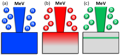
The irradiation with neutrons generates a homogeneous distribution of silicon vacancies in bulk crystals (Fig. 1a). In combination with high irradiation fluences, this method allows to create high-density ensembles, as required for the realization of room-temperature masers Kraus et al. (2014a) and highly sensitive magnetic field sensors Simin et al. (2016). Since neutrons are not charged, they lose almost all of their energy in collisions with nuclei in the lattice and hence considerably damage the SiC crystal. This leads to the creation of a multitude of defect types other than up to the formation of defect clusters, resulting in a deterioration of the coherence properties.
A more gentle approach is electron irradiation (Fig. 1b) as a large part of their energy is lost in interactions with crystal electrons. However, the electron damage cannot (in reasonable beam time with common accelerators) reach the quantum center densities achievable after irradiation with neutrons in nuclear reactors. Furthermore, the electron irradiation leads to a quantum center density gradient in the sample, with highest density close to the surface. The electron penetration depth depends on its kinetic energy. For thin samples (up to ) and -electron energy, the inhomogeneity of the in-depth defect distribution is marginal and can be neglected Campbell and Mainwood (2000). However for thick () samples, the in-depth inhomogeneous distribution should be taken into account. The samples in this study have a thickness of about .
In contrast to the aforementioned methods, ions show an increasing stopping power for lower energies according to the Bethe-Bloch equation Sigmund (2006). This results in the formation of a defect layer at a depth corresponding to the so-called Bragg peak (Fig. 1c). This approach can be used to write 3D defect structures in a SiC crystal using a focussed ion beam Kraus et al. (2017), allowing the creation of defect spins in the desired place of a nanostructure. On the other hand, the ion irradiation is not suitable for the creation of defect spin ensembles with an in-depth homogeneous distribution.
Any type of irradiation results in the creation of various types of defects, which also change the coherence properties of the vacancy-related spins. The impact of the irradiation on the and times, in spite of their crucial importance for quantum applications, has not been systematically investigated so far. In this work, we compare the spin relaxation and spin coherence in SiC created by neutron, electron and proton irradiation. Particularly, and times are measured in a broad range of the density of optically active quantum centers in the infrared regime (from here on referred to as emitter density ), from dense ensembles down to isolated defects. To improve the coherence of the defects after irradiation, we also examine the influence of sample annealing. Our results allow to predict the spin coherence properties depending on the irradiation type applied, fluence and particle energy as well as to optimize the irradiation parameters for a variety of quantum applications.
Results
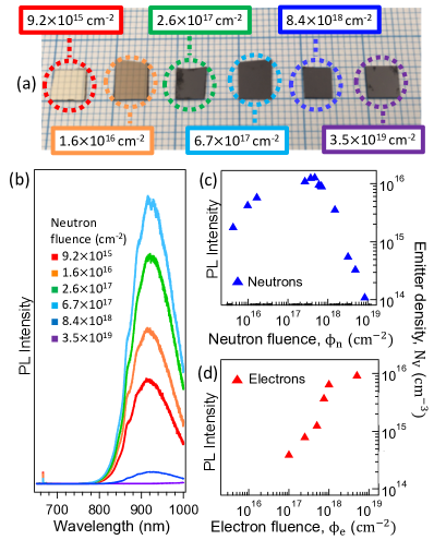
Figure 2a shows the modification of the optical properties of a SiC crystal with increasing neutron irradiation fluence. The irradiation was performed in nuclear research reactors. Since thermal neutrons only produce negligible displacement, only epithermal and fast (MeV) neutrons are counted in the fluence calculation Wendler et al. (2012). In our experiments, we use commercial high-purity semi-insulating (HPSI) 4H-SiC wafers. SiC is a wide bandgap semiconductor with a bandgap of and is therefore transparent in case of the lowest neutron fluence . Neutron irradiation creates a variety of optically active and inactive defects, which has a direct effect on the optical properties of the crystal due to absorption and scattering of light by the defects. High irradiation fluences cause crystal destruction and in case of the highest neutron fluence , SiC becomes completely opaque. The generation of the defects is verified by their characteristic room-temperature photoluminescence (PL) band in the near infrared (NIR) spectral range of Hain et al. (2014), as shown in Fig. 2b. The PL intensity shows non-monotonic behavior with the irradiation fluence. This is because high irradiation fluences lead to crystal damage and the creation of other types of defects (including defect clusters) providing non-luminescent relaxation paths for the defects.
To find the emitter density , we calibrate the PL intensity in our confocal setup with a defined collection volume using a 4H-SiC sample with known Fuchs et al. (2015). Figure 2c presents the concentration of the optically active defects as a function of the neutron fluence, which is varied over more than three orders of magnitude. The maximum is observed for and dramatically drops down for the higher neutron fluences. The electron irradiated samples reveal qualitatively similar behavior. Figure 2d presents as a function of the electron fluence for an electron energy of . The maximum is achieved for . A higher than is required to achieve the respective maximum in our samples, pointing at a lower creation yield in case of electron irradiation compared to neutron irradiation.
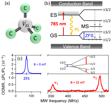
The crystallographic configuration is schematically presented in Fig. 3a. The capture of an electron by a silicon vacancy, in addition to the four electrons from the surrounding carbon atoms leads to a negatively charged state. Only this charge configuration of is optically active in NIR. Two of the total five electrons build a spin singlet and the three remaining electrons form a spin quadruplet with Kraus et al. (2014a). Upon laser excitation at , the radiative recombination from the excited state (ES) to the ground state (GS) leads to the characteristic NIR PL of the defects, as presented in the energetic structure of Fig. 3b. There are two types of the defect in the 4H-SiC polytype, referred to as V1 and V2 centers Sörman et al. (2000).
In this study, we concentrate on the V2 center with the characteristic zero-phonon line (ZFL) at and the zero-field splitting (ZFS) of between the GS spin sublevels and . There is also spin-dependent recombination from the ES to the GS through a metastable state (MS), resulting in the preferential population of the spin sublevel (Fig. 3b). The PL intensity is higher for the spin state, which is the basis for the optically detected magnetic resonance (ODMR) experiments with microwave (MW) induced transitions between the GS spin sublevels Kraus et al. (2014b). In the absence of an external magnetic field (), the ZFS can directly be observed in the ODMR spectrum (Fig. 3c). The ODMR contrast is calculated as the MW induced PL change () divided by the PL intensity, i.e., . In an external magnetic field (), the GS spin sublevels are split as shown in the inset of Fig. 3c. This results in two ODMR lines at the MW frequencies , where is the electron gyromagnetic ratio. An example of an ODMR spectrum at is shown in Fig. 3c.
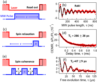
To measure the coherence properties of the spins at room temperature, we use pulsed ODMR as schematically presented in Figs. 4a, c and e. The pulse sequences are described in detail in earlier works Simin et al. (2017); Soltamov et al. (2019). The first laser pulse is used to initialize the system into the state. It is followed by a MW pulse to drive the spin transition between the and spin sublevels (inset of Fig. 3c). We apply a magnetic field along the -axis of the 4H-SiC crystal to suppress the heteronuclear-spin flip-flop processes and hence the decoherence Yang et al. (2014); Seo et al. (2016). The second laser pulse is used to reinitialize the system and read out the spin states of the defects. For this purpose, , which corresponds to the spin states of the defects, is detected immediately after the laser is switched on (dashed box in Figs. 4a, b and d). We first measure Rabi oscillations by varying the MW pulse length (Fig. 4a). An example of a measurement on an electron irradiated sample with corresponding to is presented in Fig. 4b. The fitting of these data to an exponentially decaying sine wave (solid line) allows to calibrate the MW duration for the - and -pulses.
To measure the spin-lattice relaxation time we use the protocol of Fig. 4c, where the MW -pulse is applied after the varyable delay time to exchange the spin population between the and states. The fitting of the experimental data to a mono-exponential decay of gives the spin relaxation time Widmann et al. (2015). A fitting example is shown in Fig. 4d by the solid line. We note that the spin relaxation time between the and states is expected to be shorter Soltamov et al. (2019).
To measure the spin coherence time , we use the spin echo sequence presented in Fig. 4e. The first -pulse creates a coherent superposition of the and states. It is followed by a -pulse to refocus the spin coherence after dephasing and the last -pulse to project the created superposition to an optically readable state. An example of the experimental data is presented in Fig. 4f. In addition to an exponential decay, the signal is modulated with a few frequency components, known as the electron spin-echo envelope modulation (ESEEM). These modulations have been shown to arise through hyperfine interactions between the defect spins and the surrounding and nuclei Widmann et al. (2015); Christle et al. (2015); Carter et al. (2015). In case of , the modulation frequencies and modulation amplitudes reveal a complex magnetic field dependence. To fit the experimental data, we use the product of oscillating functions decaying as . The details of the fitting procedure are described elsewhere Simin et al. (2017). An example of such a fit (solid line), from which we determine is shown in Fig. 4f.
Discussion
Effect of irradiation
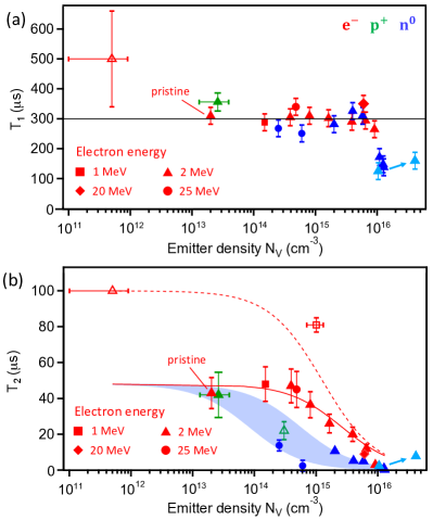
Figure 5a summarizes the measurements of the spin-lattice relaxation time as a function of the emitter density () in electron, neutron and proton irradiated samples. It is quite robust against irradiation for all irradiation types up to and equals . Remarkably, the electron energy in the range from to has no effect on . The spin relaxation is dominated by the Raman mechanism of spin-phonon scattering Simin et al. (2017); Poshakinskiy and Astakhov (2019), which is an intrinsic property of a SiC crystal and hence independent of the irradiation fluence. This result corresponds well to reported for a single defect in a sample with Widmann et al. (2015). In case of higher emitter density, the spin relaxation is given by the interaction with surrounding defects and the time decreases rapidly with .
The spin coherence time reveals strong dependence on the irradiation fluence as shown in Fig. 5b. The spin decoherence is governed by interactions with the surrounding spin bath of nuclei (, ) , paramagnetic centers (particularly ) as well as residual (particularly carbon vacancies) and irradiation-induced defects Yang et al. (2014); Carter et al. (2015); Stanwix et al. (2010). The resulting spin decoherence rate is then . By applying a moderate magnetic field is suppressed Yang et al. (2014). We assume that is proportional to the number of all irradiation induced defects, which in turn scales with . Under this assumption, the effect of irradiation can be described by
| (1) |
Here, is the spin coherence time in a pristine, non-irradiated sample given by the presence of residual paramagnetic centers and nuclear spins. It is therefore depending on the intrinsic properties and quality of a wafer. The coefficient describes the assumed proportionality .
We now discuss the experimental data for in the electron irradiated samples presented in Fig. 5b. As in case of the time, we do not find any significant dependence on the electron energy. In our HPSI wafers (solid symbols) with low irradiation fluence (, ), the time is nearly independent of . The experimental data can be well fitted to Eq. (1) with and (solid line in Fig. 5b). A deviation towards lower values is observed for , which correlates with the shortening in Fig. 5a.
The spin coherence in some other SiC samples (open symbols in Fig. 5b) was reported to be longer. It is for a single with in an epitaxial 4H-SiC layer Widmann et al. (2015). Another HPSI 4H-SiC wafer after electron irradiation gives Carter et al. (2015). As was not reported for this wafer, we assume the same creation yield as in Fig. 2d and obtain . The longer coherence time is likely related to lower concentration of intrinsic paramagnetic centers and hence longer compared to that in our non-irradiated wafer (Fig. 5b). The dashed line in Fig. 5b represents a fit to Eq. (1) with and the same as in the case above.
Compared to electron irradiation, neutron irradiation creates a higher defect density, but also a higher percentage of defects other than , resulting in a larger . As a consequence, the coherence time is significantly shorter for a moderate concentration of the created centers. The coherence time measured for the neutron-irradiated samples should be seen as a lower bound, due to inhomogeneity in the applied microwave field across the detection volume. Application of optimized pulses will be required to test the limits of coherence in such samples Nöbauer et al. (2015). Figure 5b shows experimental data for HPSI 4H-SiC wafers irradiated in two scientific reactors with different distribution of neutron energy. They can be described assuming and and the same as for our electron irradiated wafer, which is represented by the cyan area in Fig. 5b.
We now compare the aforementioned results to the spin coherence time in ion-irradiated samples. The ion irradiation can also damage the SiC lattice resulting in a reduction of . It is expected that the irradiation induced damage is stronger for heavier atoms. From this point of view, it is advantageous to use light atoms – particularly H (protons) – for the creation of highly coherent centers. In case of low proton irradiation fluence corresponding to (Fig. 5b), the coherence time approaches that in the pristine wafer Kraus et al. (2017). It was found in another work that with increasing and the time decreases. For with estimated emitter density , the spin coherence time from a stretched exponential fit was reported Embley et al. (2017).
In fact, the dependence of the spin coherence on the proton (or any other ion) irradiation flucence is more complex as in case of electron or neutron irradiation. The ions penetrate to a certain depth, which depends on their energy and the ion type. Though the highest probability to create defects is at the Bragg peak, there is a non-zero probability to create shallow centers, which have longer coherence time Brereton et al. (2018). We expect that Eq. 1 can still be used for ion irradiation though the parameter should depend on the ion type and energy as well as on the depth from the irradiated surface.
Effect of annealing
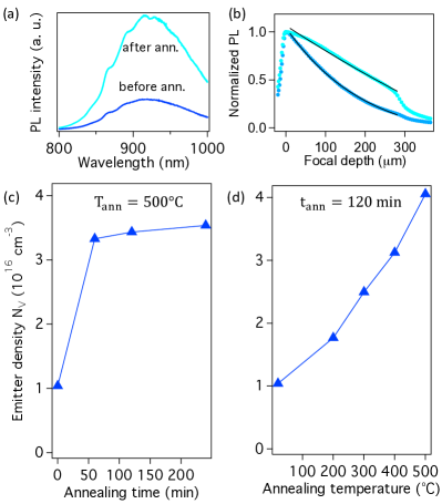
Since, as previously mentioned, a high density combined with long spin coherence is desirable for various applications, we anneal a heavily irradiated sample to explore crystal healing. Figure 6a shows the PL spectrum in a neutron irradiated sample with a fluence and the corresponding initial emitter density . Figures 6c and 6d show the emitter density as a function of the annealing time and temperature , respectively. The PL intensity linked to increases by a factor of 4 after optimum annealing conditions. This increase can be explained by healing of some irradiation-induced and intrinsic defects other than , which can provide non-radiative recombination paths for the defects if they are located in their vicinity. This conclusion is also confirmed by the in-depth (along the direction) PL scans, presented in Fig. 6b. Exponential fits to allow to estimate the absorption coefficient . It decreases from to after annealing, indicating that some color centers are indeed removed.
The annealing temperature in our experiments is limited to since the defects can otherwise be eliminated at higher temperatures Fuchs et al. (2015). We would like to note that we do neither observe any PL enhancement nor an inrease of or in the electron irradiated sample. This again strongly hints at less severe crystal damage and a higher percentage of created centers by electron irradiation.
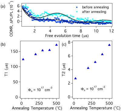
To explore the effect of annealing on the coherence properties of the defects, we measure and in the sample after each annealing step. Figure 7a shows the spin-echo experimental data before and after annealing (symbols), fitted with ESEEM (the solid lines). An improvement of the coherence properties with annealing can be clearly seen from these data.
Figure 7b presents the measured spin relaxation time as a function of the annealing temperature (). Though increases, it is not completely restored to the value of as in case of low irradiation fluences (Fig. 5a). We note, as a function of does not saturate in our experiments. For higher , might increase further, but would drop due to healing out of the defects. The spin coherence time can be improved by a factor of 2.5 as presented in Fig. 7c. The maximum value achieved in the heavily irradiated sample is . Since scales with the number of all created defects, this increase of can be explained by healing of paramagnetic, non- defects at temperatures below and therefore a suppression of decoherence caused by the spin-spin interaction.
To conclude, we have thoroughly investigated the irradiation impact on the room-temperature spin coherence properties of silicon vacancies in SiC. We have measured the spin-lattice relaxation time and the spin coherence time depending on the irradiation particle (electron, neutron and proton), irradiation fluence and irradiation energy. In order to find the broader systematics, we have analyzed the available literature values, too.
We have established, that the spin-lattice relaxation time remains constant up to high irradiation fluences, independently of the irradiation type. On the contrary, the spin coherence time is very sensitive to the irradiation type and fluence. The longest spin coherence time for the same emitter density is observed for electron irradiation. Surprisingly, the electron energy has no influence on the silicon vacancy coherence properties and all data can be well described by the same equation with two independent parameters. The shortest spin coherence time was observed in neutron-irradiated samples, which, however, can be partially recovered using thermal annealing. We thus expect that our study provides important information for the optimization of the defect spin coherence properties and allows to design quantum devices and structures with the desired parameters based on SiC as a platform.
Methods
Neutron irradiation was performed in two different research reactors. For the first irradiation set, we purchased a high-purity semi-insulating (HPSI) SiC wafer from CREE and used chambers DBVK and DBVR at the BER II reactor at Helmholtz-Zentrum Berlin. Since thermal neutrons produce negligible displacement, only epithermal and fast neutrons are counted in the fluence calculation Wendler et al. (2012). The neutron fluence spanned a large range from to . For the second irradiation set, we purchased a HPSI SiC wafer from Norstel and used the TRIGA Mark II reactor (General Atomics, San Diego) of the Atominstitut, TU Wien Fuchs et al. (2015). During irradiation, the temperature of the crystals did not exceed C. Vacancy creation by neutron irradiation in SiC is weakly dependent on neutron energy in the range MeVMeV, but falls off rapidly for smaller energies. The neutron energies in the TRIGA reactor are distributed evenly in the range between 100 eV and eV, with a peak in flux density around MeV followed by a sharp cut-off.
For the electron irradiated sample series, a HPSI 4H-SiC wafer was purchased from Norstel and diced in many pieces. The irradiation with electron energies of 1 and 2 MeV was performed at electron beam irradiation facility at QST Takasaki (Japan). During the irradiation, the samples were placed on a water cooled copper plate to avoid heating by the electron beams. The irradiation with electron energies of 20 and 25 MeV was performed at the electron accelerator ELBE in HZDR (Germany). The beam was extracted through a 300 Beryllium vacuum window and passes 150 mm through air before hitting the sample. The incident beam distribution and the small angle scattering in the vacuum window and air leads to a Gaussian shaped beam distribution on the sample. The beam profile was measured at the position of the sample with a Roos ionisation chamber (IC) N34001. The certificate calibrated IC and a Faraday cup were used for the dose and current calibration. From the profile measurement, the irradiation parameters were deduced. To monitor the current stability of the electron gun as well as dark current contributions, the edge field of the beam was constantly measured and stabilized during the irradiation.
Proton irradiation was done at the TIARA irradiation facilities in Takasaki, Japan. A piece of a 4H-SiC wafer purchased from CREE was placed on an aluminum plate and irradiated with a focused proton beam generated by a single-ended particle accelerator with a typical spot size of and proton energy of MeV. The irradiation beam current was monitored by a beam dump (Faraday cup) connected to a picoampermeter before and after irradiation.
The continuous wave and pulsed ODMR measurements were performed with a confocal setup. For optical excitation, a 788 nm diode laser (LD785-SE400 from Thorlabs) was coupled into a 50 optical fiber and focused onto the sample using a objective (Olympus LMPLN10XIR), with the laser spot measuring approximately 10 m in diameter. The laser power at the surface of the sample was about 20 mW, illuminating a volume of approximately 300 for the measurements of electron and neutron irradiated samples. For the measurement of the proton irradiated sample, a objective (Olympus LCPLN100XIR) was used, which leads to laser illumination of approx. . The PL was collected through the same objective and separated from the scattered laser light using a 850 nm short pass dichroic mirror and a 875 nm long pass filter. Behind the filter, it was coupled into a 600 optical fibre and detected using a Si avalanche photodiode (APD120A from Thorlabs). The sample was placed on a 0.5 mm copper-stripline to apply the microwaves generated by a signal generator (Stanford Research Systems SG384) and amplifier (Vectawave VBA1000-18). A permanent magnet was mounted below the sample to generate the external magnetic field of 15 mT. To generate the laser pulses needed for time-resolved ODMR experiments, an acousto-optic modulator (Opto-Electronic MT250-A02-800) was placed in the laser beam path. The microwaves were modulated using an RF-switch (Mini-Circuits ZASWA-2-50DR+). TTL pulsing for laser and microwave modulation was provided by a PulseBlaster ESR-PRO 500 MHz card from SpinCore. The ODMR signal was processed using either a lock-in amplifier (Signal Recovery DSP 7230) or an oscilloscope card from GaGe CompuScope (Razor Max).
Acknowledgments
This work has been supported by the German Research Foundation (DFG) under Grants AS 310/5-1 and DY 18/13-1, the FWF project I 3167-N27 SiC-EiC as well as JSPS KAKENHI 17H01056 and 18H03770. HK states that part of this work was carried out at the Jet Propulsion Laboratory, California Institute of Technology, under a contract with the National Aeronautics and Space Administration; and acknowledges funding by the NASA Postdoctoral Program. We thank M. Villa and R. Bergmann for operation of the TRIGA reactor as well as G. Bukalis for operation of the BER II reactor.
References
- Baranov et al. (2011) P. G. Baranov, A. P. Bundakova, A. A. Soltamova, S. B. Orlinskii, I. V. Borovykh, R. Zondervan, R. Verberk, and J. Schmidt, Silicon vacancy in SiC as a promising quantum system for single-defect and single-photon spectroscopy, Physical Review B 83, 125203 (2011).
- Koehl et al. (2011) W. F. Koehl, B. B. Buckley, F. J. Heremans, G. Calusine, and D. D. Awschalom, Room temperature coherent control of defect spin qubits in silicon carbide, Nature 479, 84 (2011).
- Riedel et al. (2012) D. Riedel, F. Fuchs, H. Kraus, S. Väth, A. Sperlich, V. Dyakonov, A. Soltamova, P. Baranov, V. Ilyin, and G. V. Astakhov, Resonant Addressing and Manipulation of Silicon Vacancy Qubits in Silicon Carbide, Physical Review Letters 109, 226402 (2012).
- Weber et al. (2010) J. R. Weber, W. F. Koehl, J. B. Varley, A. Janotti, B. B. Buckley, C. G. Van de Walle, and D. D. Awschalom, Quantum computing with defects, Proceedings of the National Academy of Sciences 107, 8513 (2010).
- Falk et al. (2013) A. L. Falk, B. B. Buckley, G. Calusine, W. F. Koehl, V. V. Dobrovitski, A. Politi, C. A. Zorman, P. X. L. Feng, and D. D. Awschalom, Polytype control of spin qubits in silicon carbide, Nature Communications 4, 1819 (2013).
- Yang et al. (2014) L.-P. Yang, C. Burk, M. Widmann, S.-Y. Lee, J. Wrachtrup, and N. Zhao, Electron spin decoherence in silicon carbide nuclear spin bath, Physical Review B 90, 241203 (2014).
- Carter et al. (2015) S. G. Carter, Ö. O. Soykal, P. Dev, S. E. Economou, and E. R. Glaser, Spin coherence and echo modulation of the silicon vacancy in 4H-SiC at room temperature, Physical Review B 92, 161202 (2015).
- Seo et al. (2016) H. Seo, A. L. Falk, P. V. Klimov, K. C. Miao, G. Galli, and D. D. Awschalom, Quantum decoherence dynamics of divacancy spins in silicon carbide, Nature Communications 7, 12935 (2016).
- Simin et al. (2017) D. Simin, H. Kraus, A. Sperlich, T. Ohshima, G. V. Astakhov, and V. Dyakonov, Locking of electron spin coherence above 20 ms in natural silicon carbide, Physical Review B 95, 161201(R) (2017).
- Fischer et al. (2018) M. Fischer, A. Sperlich, H. Kraus, T. Ohshima, G. V. Astakhov, and V. Dyakonov, Highly Efficient Optical Pumping of Spin Defects in Silicon Carbide for Stimulated Microwave Emission, Physical Review Applied 9, 2126 (2018).
- Brereton et al. (2018) P. G. Brereton, D. Puent, J. Vanhoy, E. R. Glaser, and S. G. Carter, Spin coherence as a function of implantation depth for silicon vacancies in proton-irradiated 4H-SiC, arXiv:1812.10432 .
- Soltamov et al. (2019) V. A. Soltamov, C. Kasper, A. V. Poshakinskiy, A. N. Anisimov, E. N. Mokhov, A. Sperlich, S. A. Tarasenko, P. G. Baranov, G. V. Astakhov, and V. Dyakonov, Excitation and coherent control of spin qudit modes in silicon carbide at room temperature, Nature Communications 10, 1678 (2019).
- Kraus et al. (2014a) H. Kraus, V. A. Soltamov, D. Riedel, S. Väth, F. Fuchs, A. Sperlich, P. G. Baranov, V. Dyakonov, and G. V. Astakhov, Room-temperature quantum microwave emitters based on spin defects in silicon carbide, Nature Physics 10, 157 (2014a).
- Falk et al. (2014) A. L. Falk, P. V. Klimov, B. B. Buckley, V. Ivády, I. A. Abrikosov, G. Calusine, W. F. Koehl, A. Gali, and D. D. Awschalom, Electrically and Mechanically Tunable Electron Spins in Silicon Carbide Color Centers, Physical Review Letters 112, 187601 (2014).
- Soykal and Reinecke (2017) Ö. O. Soykal and T. L. Reinecke, Quantum metrology with a single spin-3/2 defect in silicon carbide, Physical Review B 95, 081405 (2017).
- Castelletto et al. (2013a) S. Castelletto, B. C. Johnson, and A. Boretti, Quantum Effects in Silicon Carbide Hold Promise for Novel Integrated Devices and Sensors, Advanced Optical Materials 1, 609 (2013a).
- Kraus et al. (2014b) H. Kraus, V. A. Soltamov, F. Fuchs, D. Simin, A. Sperlich, P. G. Baranov, G. V. Astakhov, and V. Dyakonov, Magnetic field and temperature sensing with atomic-scale spin defects in silicon carbide, Scientific Reports 4, 5303 (2014b).
- Simin et al. (2015) D. Simin, F. Fuchs, H. Kraus, A. Sperlich, P. G. Baranov, G. V. Astakhov, and V. Dyakonov, High-Precision Angle-Resolved Magnetometry with Uniaxial Quantum Centers in Silicon Carbide, Physical Review Applied 4, 014009 (2015).
- Lee et al. (2015) S.-Y. Lee, M. Niethammer, and J. Wrachtrup, Vector magnetometry based on S=3/2 electronic spins, Physical Review B 92, 115201 (2015).
- Simin et al. (2016) D. Simin, V. A. Soltamov, A. V. Poshakinskiy, A. N. Anisimov, R. A. Babunts, D. O. Tolmachev, E. N. Mokhov, M. Trupke, S. A. Tarasenko, A. Sperlich, P. G. Baranov, V. Dyakonov, and G. V. Astakhov, All-Optical dc Nanotesla Magnetometry Using Silicon Vacancy Fine Structure in Isotopically Purified Silicon Carbide, Physical Review X 6, 031014 (2016).
- Niethammer et al. (2016) M. Niethammer, M. Widmann, S.-Y. Lee, P. Stenberg, O. Kordina, T. Ohshima, N. T. Son, E. Janzén, and J. Wrachtrup, Vector Magnetometry Using Silicon Vacancies in 4H-SiC Under Ambient Conditions, Physical Review Applied 6, 034001 (2016).
- Cochrane et al. (2016) C. J. Cochrane, J. Blacksberg, M. A. Anders, and P. M. Lenahan, Vectorized magnetometer for space applications using electrical readout of atomic scale defects in silicon carbide, Scientific Reports 6, 37077 (2016).
- Anisimov et al. (2016) A. N. Anisimov, D. Simin, V. A. Soltamov, S. P. Lebedev, P. G. Baranov, G. V. Astakhov, and V. Dyakonov, Optical thermometry based on level anticrossing in silicon carbide, Scientific Reports 6, 33301 (2016).
- Castelletto et al. (2013b) S. Castelletto, B. C. Johnson, V. Ivády, N. Stavrias, T. Umeda, A. Gali, and T. Ohshima, A silicon carbide room-temperature single-photon source, Nature Materials 13, 151 (2013b).
- Fuchs et al. (2015) F. Fuchs, B. Stender, M. Trupke, D. Simin, J. Pflaum, V. Dyakonov, and G. V. Astakhov, Engineering near-infrared single-photon emitters with optically active spins in ultrapure silicon carbide, Nature Communications 6, 7578 (2015).
- Christle et al. (2015) D. J. Christle, A. L. Falk, P. Andrich, P. V. Klimov, J. u. Hassan, N. T. Son, E. Janzén, T. Ohshima, and D. D. Awschalom, Isolated electron spins in silicon carbide with millisecond coherence times, Nature Materials 14, 160 (2015).
- Widmann et al. (2015) M. Widmann, S.-Y. Lee, T. Rendler, N. T. Son, H. Fedder, S. Paik, L.-P. Yang, N. Zhao, S. Yang, I. Booker, A. Denisenko, M. Jamali, S. A. Momenzadeh, I. Gerhardt, T. Ohshima, A. Gali, E. Janzén, and J. Wrachtrup, Coherent control of single spins in silicon carbide at room temperature, Nature Materials 14, 164 (2015).
- Christle et al. (2017) D. J. Christle, P. V. Klimov, C. F. de las Casas, K. n. Sz sz, V. Iv dy, V. Jokubavicius, J. Ul Hassan, M. Syv j rvi, W. F. Koehl, T. Ohshima, N. T. Son, E. Janz n, d. m. Gali, and D. D. Awschalom, Isolated Spin Qubits in SiC with a High-Fidelity Infrared Spin-to-Photon Interface, Physical Review X 7, 021046 (2017).
- Nagy et al. (2019) R. Nagy, M. Niethammer, M. Widmann, Y.-C. Chen, P. Udvarhelyi, C. Bonato, J. u. Hassan, R. Karhu, I. G. Ivanov, N. T. Son, J. R. Maze, T. Ohshima, Ö. O. Soykal, A. Gali, S.-Y. Lee, F. Kaiser, and J. Wrachtrup, High-fidelity spin and optical control of single silicon-vacancy centres in silicon carbide, Nature Communications 10, 1954 (2019).
- Banks et al. (2018) H. B. Banks, Ö. O. Soykal, R. Myers-Ward, D. K. Gaskill, T. L. Reinecke, and S. G. Carter, Resonant optical spin initialization and readout of single silicon vacancies in 4H-SiC, arXiv:1811.01293 .
- Whiteley et al. (2019) S. J. Whiteley, G. Wolfowicz, C. P. Anderson, A. Bourassa, H. Ma, M. Ye, G. Koolstra, K. J. Satzinger, M. V. Holt, F. J. Heremans, A. N. Cleland, D. I. Schuster, G. Galli, and D. D. Awschalom, Spin–phonon interactions in silicon carbide addressed by Gaussian acoustics, Nature Physics 112, 3866 (2019).
- Poshakinskiy and Astakhov (2019) A. V. Poshakinskiy and G. V. Astakhov, Optically detected spin-mechanical resonance in silicon carbide membranes, arXiv:1903.00876 .
- Calusine et al. (2014) G. Calusine, A. Politi, and D. D. Awschalom, Silicon carbide photonic crystal cavities with integrated color centers, Applied Physics Letters 105, 011123 (2014).
- Bracher and Hu (2015) D. O. Bracher and E. L. Hu, Fabrication of High-Q Nanobeam Photonic Crystals in Epitaxially Grown 4H-SiC, Nano Letters 15, 6202 (2015).
- Radulaski et al. (2017) M. Radulaski, M. Widmann, M. Niethammer, J. L. Zhang, S.-Y. Lee, T. Rendler, K. G. Lagoudakis, N. T. Son, E. Janzén, T. Ohshima, J. Wrachtrup, and J. Vučković, Scalable Quantum Photonics with Single Color Centers in Silicon Carbide, Nano Letters 17, 1782 (2017).
- Lohrmann et al. (2017) A. Lohrmann, T. J. Karle, V. K. Sewani, A. Laucht, M. Bosi, M. Negri, S. Castelletto, S. Prawer, J. C. McCallum, and B. C. Johnson, Integration of Single-Photon Emitters into 3C-SiC Microdisk Resonators, ACS Photonics 4, 462 (2017).
- Fuchs et al. (2013) F. Fuchs, V. A. Soltamov, S. Väth, P. G. Baranov, E. N. Mokhov, G. V. Astakhov, and V. Dyakonov, Silicon carbide light-emitting diode as a prospective room temperature source for single photons, Scientific Reports 3, 1637 (2013).
- Lohrmann et al. (2015) A. Lohrmann, N. Iwamoto, Z. Bodrog, S. Castelletto, T. Ohshima, T. J. Karle, A. Gali, S. Prawer, J. C. McCallum, and B. C. Johnson, Single-photon emitting diode in silicon carbide, Nature Communications 6, 7783 (2015).
- Niethammer et al. (2019) M. Niethammer, M. Widmann, T. Rendler, N. Morioka, Y.-C. Chen, R. Stöhr, J. u. Hassan, S. Onoda, T. Ohshima, S.-Y. Lee, A. Mukherjee, J. Isoya, N. T. Son, and J. Wrachtrup, Coherent electrical readout of defect spins in 4H-SiC by photo-ionization at ambient conditions, arXiv:1903.12236 .
- Castelletto et al. (2014) S. Castelletto, B. C. Johnson, C. Zachreson, D. Beke, I. Balogh, T. Ohshima, I. Aharonovich, and A. Gali, Room Temperature Quantum Emission from Cubic Silicon Carbide Nanoparticles, ACS Nano 8, 7938 (2014).
- Muzha et al. (2014) A. Muzha, F. Fuchs, N. V. Tarakina, D. Simin, M. Trupke, V. A. Soltamov, E. N. Mokhov, P. G. Baranov, V. Dyakonov, A. Krueger, and G. V. Astakhov, Room-temperature near-infrared silicon carbide nanocrystalline emitters based on optically aligned spin defects, Applied Physics Letters 105, 243112 (2014).
- Chen et al. (2018) Y.-C. Chen, P. S. Salter, M. Niethammer, M. Widmann, F. Kaiser, R. Nagy, N. Morioka, C. Babin, J. ü. Erlekampf, P. Berwian, M. Booth, and J. ö. Wrachtrup, Laser writing of scalable single colour centre in silicon carbide, arXiv:1812.04284 .
- Sörman et al. (2000) E. Sörman, N. Son, W. Chen, O. Kordina, C. Hallin, and E. Janzén, Silicon vacancy related defect in 4H and 6H SiC, Physical Review B 61, 2613 (2000).
- von Bardeleben et al. (2000a) H. J. von Bardeleben, J. L. Cantin, L. Henry, and M. F. Barthe, Vacancy defects in p-type 6H-SiC created by low-energy electron irradiation, Physical Review B 62, 10841 (2000a).
- Heinisch et al. (2004) H. L. Heinisch, L. R. Greenwood, W. J. Weber, and R. E. Williford, Displacement damage in silicon carbide irradiated in fission reactors, Journal of Nuclear Materials 327, 175 (2004).
- von Bardeleben et al. (2000b) H. von Bardeleben, J. Cantin, I. Vickridge, and G. Battistig, Proton-implantation-induced defects in n-type 6H- and 4H-SiC: An electron paramagnetic resonance study, Physical Review B 62, 10126 (2000b).
- Kraus et al. (2017) H. Kraus, D. Simin, C. Kasper, Y. Suda, S. Kawabata, W. Kada, T. Honda, Y. Hijikata, T. Ohshima, V. Dyakonov, and G. V. Astakhov, Three-Dimensional Proton Beam Writing of Optically Active Coherent Vacancy Spins in Silicon Carbide, Nano Letters 17, 2865 (2017).
- Wang et al. (2017a) J. Wang, X. Zhang, Y. Zhou, K. Li, Z. Wang, P. Peddibhotla, F. Liu, S. Bauerdick, A. Rudzinski, Z. Liu, and W. Gao, Scalable Fabrication of Single Silicon Vacancy Defect Arrays in Silicon Carbide Using Focused Ion Beam, ACS Photonics 4, 1054 (2017a).
- Wang et al. (2017b) J. Wang, Y. Zhou, X. Zhang, F. Liu, Y. Li, K. Li, Z. Liu, G. Wang, and W. Gao, Efficient Generation of an Array of Single Silicon-Vacancy Defects in Silicon Carbide, Physical Review Applied 7, 064021 (2017b).
- Embley et al. (2017) J. S. Embley, J. S. Colton, K. G. Miller, M. A. Morris, M. Meehan, S. L. Crossen, B. D. Weaver, E. R. Glaser, and S. G. Carter, Electron spin coherence of silicon vacancies in proton-irradiated 4H-SiC, Physical Review B 95, 045206 (2017).
- Wang et al. (2018) J.-F. Wang, Q. Li, F.-F. Yan, H. Liu, G.-P. Guo, W.-P. Zhang, X. Zhou, Z.-H. Lin, J.-M. Cui, X.-Y. Xu, J.-S. Xu, C.-F. Li, and G.-C. Guo, On-demand generation of shallow silicon vacancy in silicon carbide, arXiv:1810.11252 .
- Campbell and Mainwood (2000) B. Campbell and A. Mainwood, Radiation Damage of Diamond by Electron and Gamma Irradiation, physica status solidi (a) 181, 99 (2000).
- Sigmund (2006) P. Sigmund, Particle Penetration and Radiation Effects, Springer Series in Solid-State Sciences, Vol. 151 (Springer Berlin Heidelberg, Berlin, Heidelberg, 2006).
- Wendler et al. (2012) E. Wendler, T. Bierschenk, F. Felgenträger, J. Sommerfeld, W. Wesch, D. Alber, G. Bukalis, L. C. Prinsloo, N. van der Berg, E. Friedland, and J. B. Malherbe, Damage formation and optical absorption in neutron irradiated SiC, Nuclear Instruments and Methods in Physics Research Section B: Beam Interactions with Materials and Atoms 286, 97 (2012).
- Hain et al. (2014) T. C. Hain, F. Fuchs, V. A. Soltamov, P. G. Baranov, G. V. Astakhov, T. Hertel, and V. Dyakonov, Excitation and recombination dynamics of vacancy-related spin centers in silicon carbide, Journal of Applied Physics 115, 133508 (2014).
- Stanwix et al. (2010) P. L. Stanwix, L. M. Pham, J. R. Maze, D. Le Sage, T. K. Yeung, P. Cappellaro, P. R. Hemmer, A. Yacoby, M. D. Lukin, and R. L. Walsworth, Coherence of nitrogen-vacancy electronic spin ensembles in diamond, Physical Review B 82, 201201 (2010).
- Nöbauer et al. (2015) T. Nöbauer, A. Angerer, B. Bartels, M. Trupke, S. Rotter, J. Schmiedmayer, F. Mintert, and J. Majer, Smooth Optimal Quantum Control for Robust Solid-State Spin Magnetometry, Physical Review Letters 115, 190801 (2015).