Macroscopic electron-hole distribution in silicon and cubic silicon carbide
Abstract
Electron excitations at silicon and 3C-SiC surfaces caused by an intense femtosecond laser pulse can be calculated by solving the time-dependent density functional theory and the Maxwell’s equation simultaneously. The energy absorption, carrier density, and electron-hole quasi-temperatures decrease exponentially in 100 nm from the surface. The electron and hole quasi-temperatures have finite values even at large distances from the surface because of a specific photo-absorption channel. Although the quasi-temperature in the silicone shows smooth exponential descrease, 3C-SiC shows stepwise decrease because of the change of concerning bands. The quasi-temperature depends not only on the excitation process, i.e., tunnel and multi-photon absorption, but also on the band structure significantly.
I introduction
Processing of solid materials using femtosecond laser pulses has attracted considerable interest for potential application to high-precision processing technology. Chichkov et al. (1996); Stuart et al. (1996); Liu, Du, and Mourou (1997); Lenzner et al. (1998); Geissler et al. (1999); Lenzner et al. (2000); Sudrie et al. (2002); Doumy et al. (2004); Amoruso et al. (2005); Gattass and Mazur (2008); Gamaly (2011); Chimier et al. (2011) Because a femtosecond laser pulse can deposit large amounts of energy into solid materials within a much shorter time than the conventional spatial diffusion of thermal energy to the exterior of the irradiated spot, we can process materials with small thermal denaturation outside of the irradiated volume.Gattass and Mazur (2008); Gamaly (2011)
The precise description of the electron-hole distribution and their quasi-temperatures are important to understand the initial stage of laser processing. The multi-photon absorption and tunnel excitation processes are the crucial electron excitation processes in semiconductors under the femtosecond laser pulse. Since these processes are nonlinear and/or nonperturbative, we have to treat the dynamics of the electron and electromagnetic fields simultaneously Li and Ki (2006); Rethfeld et al. (2017).
The two temperature model Snishimov, Kapeliovicj, and Perel’man (1975); Allen (1987) (TTM) is a common approach to describe the energy flow between an electron and phonon in metals. The TTM is applied to semiconductors and dielectrics by combining electron excitation and scattering modelsSilaeva et al. (2012); Gallais et al. (2015). Although the electron excitation process and electron-hole distribution is complicated, the excitation process and the estimation of the electron temperature assuming simple model. To understand the electron-hole state induced by a laser field around a surface, the dynamics of the electrons and electromagnetic field should be treated directly.
Recently, we developed a first-principle numerical program SALMON, which combines time-dependent density functional theory (TDDFT) and the Maxwell’s equation Noda et al. (2018). In the present work, we would like to calculate the macroscopic carrier and hole distribution at the surface of silicon and cubic silicon carbide (3C-SiC).
II Computational method
The theory and its implementation in the present calculation have been described elsewhere Bertsch et al. (2000); Yabana et al. (2012); Noda et al. (2018); therefore, we describe it briefly. The laser pulse that enters from the vacuum and attenuates in the medium varies on a scale of micrometers, while the electron dynamics take place on a subnanometer scale. To overcome these conflicting spatial scales, we have developed a multiscale implementation by introducing two coordinate systems: macroscopic coordinate for the laser pulse propagation and the microscopic coordinate for local electron dynamics. The laser pulse is described by the vector potential , which satisfies
| (1) |
At each point , we consider lattice-periodic electron dynamics driven by the electric field . They are described by the electron orbitals , which satisfy the time-dependent Kohn–Sham equation at each point Noda et al. (2018).
| (2) | |||||
where the potential , which includes Hartree and ionic contributions, and the exchange-correlation potential are periodic in the lattice. In this work, we use local density approximation (LDA) Perdew and Zunger (1981) for exchange-correlation potential in adiabatic approximation.
The electric current at , , is provided from electron orbitals as
| (3) | |||||
where is the volume of a unit cell. is the current caused by the nonlocality of pseudopotential.
We solved Eqs. (1)–(3) simultaneously as an initial value problem, where the incident laser pulse is prepared in a vacuum region in front of the surface, while all the Kohn–Sham orbitals are set to their ground state.
The incident laser field in vacuum, , is described as,
| (4) |
where is the electric field amplitude at the peak, is the laser frequency, describes the space-time dependence of the field. The pulse length is set to be 10.81 fs, and the computation is terminated at fs.
III Results
III.1 Silicon
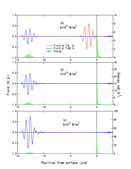
We first assume a typical silicon semiconductor. Because we use the LDA exchange-correlation potential, the calculated direct band gap (2.4 eV) is smaller than the experimental one (3.1 eV) Figure 1 shows the initial laser field (red dashed line in (a)), reflected and transmitted field (blue solid lines), and the energy density (green filled lines). We define the energy of the ground state as 0 eV/Å3.
The cubic unit cell containing eight carbon atoms was discretized into grids of 163. The Bloch -space was also discretized into 163 grid points. The macroscopic mesh size for the Maxwell Eq. (Eq. (1)) is 13 nm. The time step is set to 0.04 atomic unit (0.97 attosecond).
The absorbed energy is defined as the difference of between its initial and final values, where . The electron-hole density () is defined by the projection of the time-dependent wavefunction at onto the initial state Otobe et al. (2008).
Individual projections to the initial states at each macro point , given by,
| (5) |
give the occupation of state . We prepare adequate unoccupied states in the conduction band, typically comprising 100 states for each , to calculate the overall electron distribution.
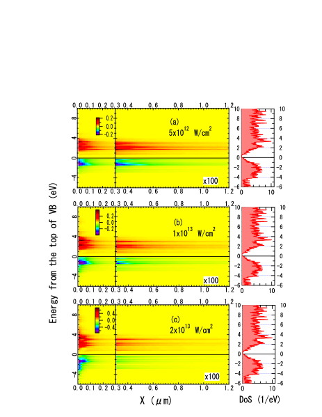
Figure 2 shows the change in the electron distribution,
| (6) |
in the form of the density of states (DoS). Red color indicates the excited electron in the conduction band (CB), whereas the blue indicates the hole in the valence band (VB). The color map in the area deeper than 0.3 is 100 times enhanced.
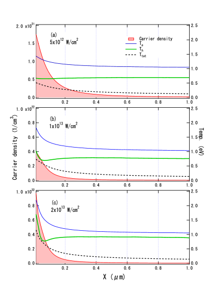
We can estimate the quasi-temperatures of the electron and hole with the QTM, and the temperature of the total system with the STM Otobe, Hayashi, and Nishikino (2017). The reduced internal energies in the conduction and valence bands, given by and , respectively, can be defined as
| (7) |
where represents the states in the valence (conduction) band, and is the energy eigenvalue of the -th state at . We can assume the quasi-temperatures of carrier () and hole () at each from , and the temperature () from the .
Figure 3 shows the carrier density, quasi-temperatures, and temperature as functions of position from the silicon surface. The color map of the density is 100 times enhanced in regions deeper than m. At the surface, the electron (red) and hole (blue) spread into a wide energy range as the laser intensity increases. However, in the region m, the electron and the hole states have specific peaks whose energy positions do not depend on the position and laser intensity.
The position-independent behavior at m and laser intensity dependence at the surface are presented in Fig. 2, and the position-dependent quasi-temperatures are shown in Fig. 3. Around the surface (m), the quasi-temperatures show an exponential decrease as increases. However, in the deeper region, the electron and hole show approximately same quasi-temperatures around 1.0 eV. It should be noted that the carrier density and the electron temperature in the STM show a monotonic decrease, as predicted by the previous models. We can also see a small dip in the hole quasi-temperature around m in Fig. 2 (b) and (c), which is the transient region between the exponential decrease and the position-independent region. This dip in the hole quasi-temperature corresponds to the intense single peak in hole density.
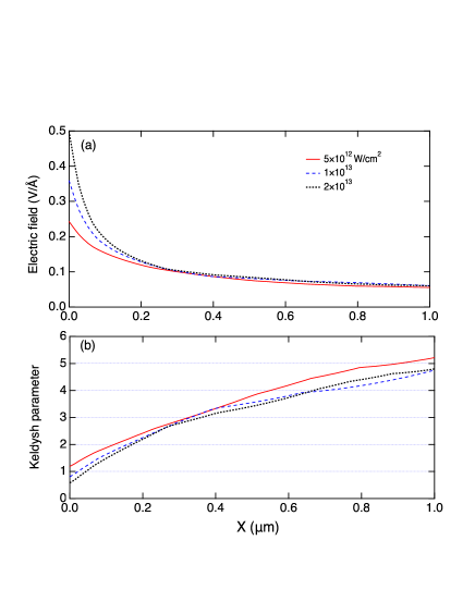
The dip in the hole quasi-temperature indicates the excitation process dependence in the electron-hole distribution. In general, the photo-excitation process can be attributed to regime, that is, multi-photon absorption and tunneling process. Since an intense laser field induces the tunneling process preferentially, the tunneling process occurs around the surface. The Keldysh parameter Keldysh (1965) is a good parameter to classify the excitation process. Here, is the effective mass, is the band gap, and is the electric field. The tunneling process (multi-photon absorption) is dominant for ().
Figure 4 shows the (a) maximum field and (b) at . While the weakest laser intensity ( W/cm2) shows for all the points, across the one around m with a laser intensity of and W/cm2. The positions of ( m) correspond to the dip in the hole quasi-temperature, as shown in Fig. 3. This result indicates that the hole and/or electron distribution change by the excitation process. The tunneling process gives a broader distribution of the electron-hole pairs, which correspond to a higher quasi-temperature. However, the multiphoton process gives specific peaks of electron-hole pairs, which correspond to the laser intensity–independent lower quasi-temperature.
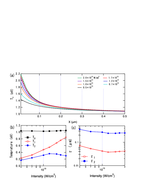
Although the hole quasi-temperature shows a complex -dependence, the electron quasi-temperature () may be approximated by the simple double exponential function,
| (8) |
because there are two different excitation processes. Here, and are the peak temperature and the damping factor at the surface, and are the parameters in a deeper region, is the parameter for saturated temperature. Figure5 (a) shows the computational results (solid lines) and fitted function (dashed lines). The fitted function well reproduces . The fitting parameters are shown in Fig. 5 (b) and (c).
does not depend on the laser intensity, which is consistent with the results in Fig. 3. is the dominant parameter at a deeper region, because is small. , which corresponds to , increases monotonically as the function of laser intensity. and are close to each other at and W/cm2. This similarity indicates that the multiphoton absorption is the dominant excitation process at such intensities. However, above W/cm2, the deviation between and indicates that a change in the excitation process occurs at the surface, as shown in Fig. 4. The damping parameter decreases as the laser intensity increases, which corresponds to the steep decrease of around the surface.
III.2 3C-SiC

SiC is attracting interest as a foundation base in the next generation, because of its wide band gap ( eV), temperature resistance, good thermal conductivity, as well as impact resistance Persson and Lindefelt (1996); Morkoç et al. (1994); Matsunami and Kimoto (1997); Son et al. (2000). However, for its hardness and chemical and mechanical stability, SiC is difficult to process. The processing by the femtosecond laser pulse enables the processing of SiC by the nonlinear processes Choi et al. (2016).
Figure 6 shows the dielectric function of 3C-SiC with LDA potential. From the imaginary part of the dielectric function (Im), the optical band gap is 4.2 eV.
In the macroscopic calculation, we discretized a cubic cell, including 4 carbon and 4 silicon atoms, into grids. We used K-sampling grids for the Bloch phase space. Eighty-four conduction bands were prepared to calculate the excited electron distribution.
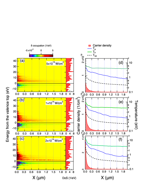
Figure 7 (a)–(c) shows the position-dependent electron-hole distribution at three different laser intensities. The hole density has a peak at -3 eV and the electron density has a peak at 3 eV at a deeper region, whose energy difference (6 eV) corresponds to four-photon absorption.
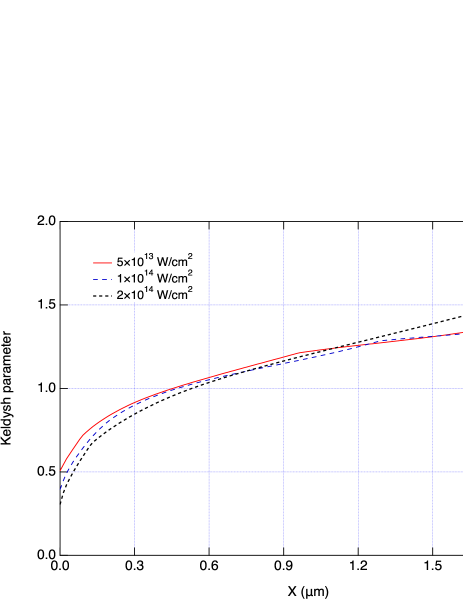
Although the quasi-temperatures of silicon show a smooth decrease with increasing , 3C-SiC shows a stepwise structure in Fig. 6 (d)–(f). The abrupt change in and corresponds to the change of the number of contributing bands. The stepwise structure indicates that the band structure affects the electron-hole distribution and temperature. However, the carrier density and show monotonic behavior as increases. At all intensities, becomes position-independent at , which corresponds to the behavior of the Keldysh parameter, as shown in Fig. 8.
While is much higher than in silicon, of 3C-SiC becomes much higher than . Although at a deeper region is 4 eV at all laser intensities, which corresponds to hole creation at same energy point, decreases as increases. From Fig. 7 (a)-(c), the electron at 5 eV survives even at a relatively deeper position (weak field intensity). These results indicate that the quasi-temperatures depend strongly on the material, in other words, band structure.
IV Summary
In summary, we studied the spatial dependence of the quasi-temperatures in silicon and 3C-SiC by employing the time-dependent Kohn–Sham equation and Maxwell equation. We found that the quasi-temperature and the electron-hole distribution depend on the excitation process. While the quasi-temperatures do not show any spatial dependence where multiphoton absorption is dominant, they increase at the surface where the tunneling excitation process is important. Although we found that the carrier quasi-temperature can be approximated by a simple double exponential function in silicon, 3C-SiC shows a stepwise spatial distribution in quasi-temperatures. These results indicate that the estimation of the quasi-temperatures from the quantum mechanical simulation is important to employ electron-lattice models, such as the two-temperature model, to understand the initial state of the laser processing and/or laser damage.
Our method treats the electron and electromagnetic field dynamics without any artificial parameters. However, we should contain lattice dynamics induced by the electron excitation, which occurs in longer time scale, to simulate the laser processing. We can understand the early stage of the laser processing by combining our method and classical molecular dynamics or fluid dynamics in the future.
Acknowledgement
This work was supported by MEXT Quantum Leap Flagship Program (MEXT Q-LEAP) Grant Number JPMXS0118067246, JST-CREST under grant number JP-MJCR16N5, and by JSPS KAKENHI Japan Grant Numbers JP17H03525. The numerical calculations were performed on the supercomputer SGI ICE X at the Japan Atomic Energy Agency (JAEA). We would like to thank Editage (www.editage.com) for English language editing.
References
- Chichkov et al. (1996) B. N. Chichkov, C. Momma, S. Nolte, F. von Alvensleben, and A. Tünnermann, Applied Physics A 63, 109 (1996).
- Stuart et al. (1996) B. C. Stuart, M. D. Feit, S. Herman, A. M. Rubenchik, B. W. Shore, and M. D. Perry, Phys. Rev. B 53, 1749 (1996).
- Liu, Du, and Mourou (1997) X. Liu, D. Du, and G. Mourou, IEEE Journal of Quantum Electronics 33, 1706 (1997).
- Lenzner et al. (1998) M. Lenzner, J. Krüger, S. Sartania, Z. Cheng, C. Spielmann, G. Mourou, W. Kautek, and F. Krausz, Phys. Rev. Lett. 80, 4076 (1998).
- Geissler et al. (1999) M. Geissler, G. Tempea, A. Scrinzi, M. Schnürer, F. Krausz, and T. Brabec, Phys. Rev. Lett. 83, 2930 (1999).
- Lenzner et al. (2000) M. Lenzner, F. Krausz, J. Krüger, and W. Kautek, Applied Surface Science 154-155, 11 (2000).
- Sudrie et al. (2002) L. Sudrie, A. Couairon, M. Franco, B. Lamouroux, B. Prade, S. Tzortzakis, and A. Mysyrowicz, Phys. Rev. Lett. 89, 186601 (2002).
- Doumy et al. (2004) G. Doumy, F. Quéré, O. Gobert, M. Perdrix, P. Martin, P. Audebert, J. C. Gauthier, J.-P. Geindre, and T. Wittmann, Phys. Rev. E 69, 026402 (2004).
- Amoruso et al. (2005) S. Amoruso, G. Ausanio, R. Bruzzese, M. Vitiello, and X. Wang, Phys. Rev. B 71, 033406 (2005).
- Gattass and Mazur (2008) R. R. Gattass and E. Mazur, Nature Photonics 2, 219 EP (2008).
- Gamaly (2011) E. Gamaly, Physics Reports 508, 91 (2011).
- Chimier et al. (2011) B. Chimier, O. Utéza, N. Sanner, M. Sentis, T. Itina, P. Lassonde, F. Légaré, F. Vidal, and J. C. Kieffer, Phys. Rev. B 84, 094104 (2011).
- Li and Ki (2006) H. Li and H. Ki, Journal of Applied Physics 100, 104907 (2006), https://doi.org/10.1063/1.2388853 .
- Rethfeld et al. (2017) B. Rethfeld, D. S. Ivanov, M. E. Garcia, and S. I. Anisimov, Journal of Physics D: Applied Physics 50, 193001 (2017).
- Snishimov, Kapeliovicj, and Perel’man (1975) S. I. Snishimov, B. L. Kapeliovicj, and T. L. Perel’man, Sov. Phys.-JETP 39, 375 (1975).
- Allen (1987) P. B. Allen, Phys. Rev. Lett. 59, 1460 (1987).
- Silaeva et al. (2012) E. P. Silaeva, A. Vella, N. Sevelin-Radiguet, G. Martel, B. Deconihout, and T. E. Itina, New Journal of Physics 14, 113026 (2012).
- Gallais et al. (2015) L. Gallais, D.-B. Douti, M. Commandré, G. Batavičiūtė, E. Pupka, M. Ščiuka, L. Smalakys, V. Sirutkaitis, and A. Melninkaitis, Journal of Applied Physics 117, 223103 (2015), https://doi.org/10.1063/1.4922353 .
- Noda et al. (2018) M. Noda, S. A. Sato, Y. Hirokawa, M. Uemoto, T. Takeuchi, S. Yamada, A. Yamada, Y. Shinohara, M. Yamaguchi, K. Iida, I. Floss, T. Otobe, K.-M. Lee, K. Ishimura, T. Boku, G. F. Bertsch, K. Nobusada, and K. Yabana, Computer Physics Communications (2018), https://doi.org/10.1016/j.cpc.2018.09.018.
- Bertsch et al. (2000) G. F. Bertsch, J.-I. Iwata, A. Rubio, and K. Yabana, Phys. Rev. B 62, 7998 (2000).
- Yabana et al. (2012) K. Yabana, T. Sugiyama, Y. Shinohara, T. Otobe, and G. F. Bertsch, Phys. Rev. B 85, 045134 (2012).
- Perdew and Zunger (1981) J. P. Perdew and A. Zunger, Phys. Rev. B 23, 5048 (1981).
- Otobe et al. (2008) T. Otobe, M. Yamagiwa, J.-I. Iwata, K. Yabana, T. Nakatsukasa, and G. F. Bertsch, Phys. Rev. B 77, 165104 (2008).
- Otobe, Hayashi, and Nishikino (2017) T. Otobe, T. Hayashi, and M. Nishikino, Applied Physics Letters 111, 171107 (2017), https://doi.org/10.1063/1.4997363 .
- Keldysh (1965) L. V. Keldysh, Sov. Phys.-JETP 20, 1307 (1965).
- Persson and Lindefelt (1996) C. Persson and U. Lindefelt, Phys. Rev. B 54, 10257 (1996).
- Morkoç et al. (1994) H. Morkoç, S. Strite, G. B. Gao, M. E. Lin, B. Sverdlov, and M. Burns, Journal of Applied Physics 76, 1363 (1994), https://doi.org/10.1063/1.358463 .
- Matsunami and Kimoto (1997) H. Matsunami and T. Kimoto, Materials Science and Engineering: R: Reports 20, 125 (1997), r20.
- Son et al. (2000) N. T. Son, P. N. Hai, W. M. Chen, C. Hallin, B. Monemar, and E. Janzén, Phys. Rev. B 61, R10544 (2000).
- Choi et al. (2016) I. Choi, H. Y. Jeong, H. Shin, G. Kang, M. Byun, H. Kim, A. M. Chitu, J. S. Im, R. S. Ruoff, S.-Y. Choi, and K. J. Lee, Nature Communications 7, 13562 EP (2016).