Exciton-polaritons in multilayer WSe2 in a planar microcavity
Abstract
Due to high binding energy and oscillator strength, excitons in thin flakes of transition metal dichalcogenides constitute a perfect foundation for realizing a strongly coupled light-matter system. In this paper we investigate mono- and few-layer WSe2 flakes encapsulated in hexagonal boron nitride and incorporated into a planar dielectric cavity. We use an open cavity design which provides tunability of the cavity mode energy by as much as 150 meV. We observe a strong coupling regime between the cavity photons and the neutral excitons in direct-bandgap monolayer WSe2, as well as in few-layer WSe2 flakes exhibiting indirect bandgap. We discuss the dependence of the exciton’s oscillator strength and resonance linewidth on the number of layers and predict the exciton-photon coupling strength.
I Introduction
The possibility to engineer multilayered structures using two-dimensional (2D) van der Waals materials allows to construct new artificial crystals of designed functionalities Geim and Grigorieva (2013) with strong application potential in photonics and opto-electronics Mak and Shan (2016), including, especially, the areas of photo-detectors, ultrathin-film photovoltaic devices, light emitting diodes and lasers Britnell et al. (2013); Koppens et al. (2014); Ahn et al. (2016); Pu and Takenobu (2018); Binder et al. (2019).
Optical properties of monolayer (ML) transition metal dichalcogenides (TMDs) are widely explored as they are dominated by particularly strong exciton resonances stable up to room temperatures Wang et al. (2018); Koperski et al. (2017). This is a consequence of their direct bandgap in contrast to few-layer and bulk forms that exhibit indirect optical transitions Splendiani et al. (2010); Mak et al. (2010); Molas et al. (2017). These properties make ML TMDs interesting for laser light sources Wu et al. (2015); Ye et al. (2015); Li et al. (2017) and light-matter interactions which demand narrow-resonance oscillators Basov et al. (2016); Schneider et al. (2018). For ML, the lowest energy transition occurs between the band-edge states at the points of the Brillouin zone, which are mostly composed of the transition metal atom orbitals: orbitals in the valence band (VB) and orbitals in the conduction band (CB). Starting from the bilayer, an indirect transition between the band-edge states at the point in the VB and the Q point in the CB appears, as those states are partially composed of orbitals of the chalcogen atoms, which significantly overlap between the layers Kormányos et al. (2015); Liu et al. (2015); Lindlau et al. (2018).
For a long time the indirect bandgap of multilayer TMDs was considered a drawback in the construction of opto-electronic devices due to low emission rate and poor quantum efficiency. However, compared to the ML, multilayers of TMDs have also several advantages as they possess larger optical density of states and exhibit higher absorbance as well as longer exciton lifetimes Li et al. (2018). It is also possible to tune the bandgap and alter the carrier type in TMD-based FET devices through the control over the TMD film thickness Pudasaini et al. (2018).
In this work, we explore the high optical absorbance of multilayer TMDs and demonstrate the strong light-matter coupling between the cavity photons and neutral excitons in multilayer WSe2 placed in a tunable, planar optical resonator. Multiple works have already demonstrated the strong coupling regime for excitons in TMD monolayers incorporated into various types of planar optical cavities Lundt et al. (2016): dielectric Liu et al. (2014), tunable Dufferwiel et al. (2018); Flatten et al. (2017), metallic Sun et al. (2017), semiconductor–metallic Waldherr et al. (2018), but all of them were entirely focused on direct-bandgap ML flakes or MLs separated by thin hexagonal boron nitride (hBN) flakes Dufferwiel et al. (2015).
The strong light-matter coupling conditions in multilayer TMDs have been recently achieved in different systems with plasmonic cavities of ultra-small volume Kleemann et al. (2017); Stührenberg et al. (2018) and in open plasmonic cavities formed by periodic arrays of metallic nanoparticles Wang et al. (2019). In that case, however, the resonant electric field is polarized perpendicularly to the flakes’ plane and nearly perpendicularly to the excitons’ dipole moment which is mostly in-plane oriented Schuller et al. (2013). Here we report on the observation of the strong coupling regime between photons confined in a planar cavity, where the electric field is polarized along the main axis of the excitons’ dipole moment, with neutral excitons in ML as well as few-layer-thick WSe2 flakes. Starting from the bilayer WSe2 the bandgap becomes indirect, but the absorption at direct excitonic resonance is efficient enough to allow for creation of strongly coupled light–matter states. The exciton–photon coupling strength reaches even higher values for multilayers than for the ML due to increased thickness of the TMD material. Our findings are well reproduced by calculations done within the framework of a transfer matrix method, where the parameters of the excitonic resonances in WSe2 are determined based on the analysis of reflectance spectra of the flakes deposited directly onto the bottom distributed Bragg reflector (DBR).
II Results
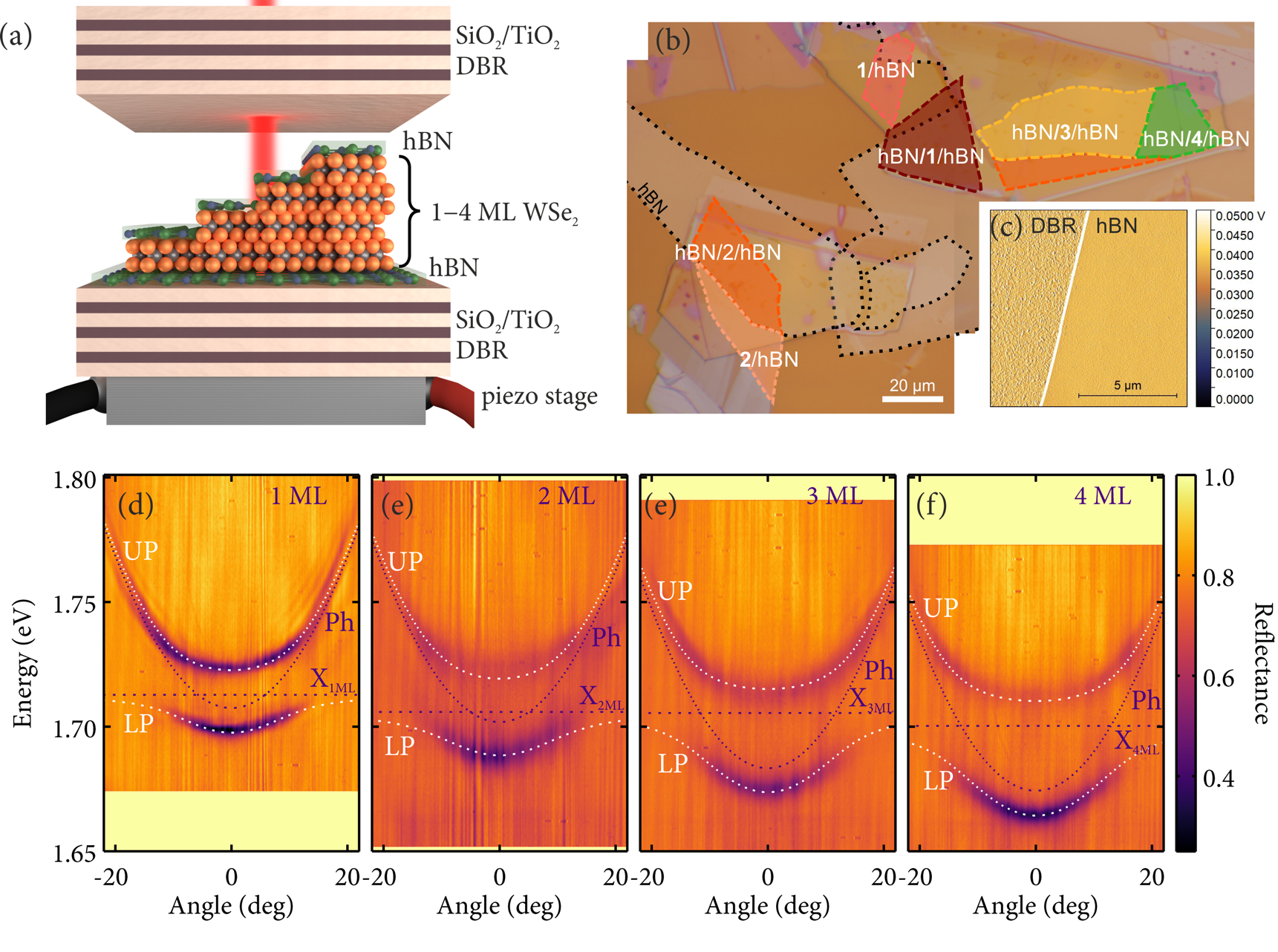
We investigated 1 ML- to 4 ML-thick WSe2 flakes embedded in an open, tunable dielectric cavity schematically shown in Fig. 1(a). The cavity consists of two dielectric distributed Bragg reflectors (DBRs), each made of 5 pairs of SiO2/TiO2 layers with the maximum reflectance at 723 nm (1.715 eV), chosen specifically to match the energy of the A exciton in monolayer WSe2 encapsulated in hBN Manca et al. (2017). The mirrors were grown on a transparent fused silica substrate to provide optical access also from the back side.
WSe2 flakes were mechanically exfoliated from commercially available, nominally undoped bulk crystals. Selected flakes of 1 to 4 ML thickness were then transferred onto approx. 183 nm thick (see Fig. S1 Supplementary Materials) hBN flakes previously deposited on top of the bottom DBR. The thickness of the bottom hBN flakes was chosen to obtain the local maximum of the electric field standing wave inside the final full cavity at the position of the WSe2 flakes to assure the efficient exciton-photon coupling conditions (see Supplementary Materials for details). The hBN capping layer covering the WSe2 flakes was much thinner, approx. 10 nm. Fig. 1(b) presents an optical microscope image of the investigated WSe2 flakes. The hBN encapsulation allows to significantly reduce the inhomogeneous broadening of spectral lines, leading to linewidths that approach the radiative decay limit Cadiz et al. (2017); Ajayi et al. (2017).
The influence of the encapsulation is still under investigation Fang et al. (2019), but hBN provides isolation of the electrostatic disorder at the SiO2 interfaces and acts also as an atomically flat substrate for the flakes. A comparison of surface roughness of the DBR and the hBN flake deposited on that DBR, measured by atomic force microscopy, is shown in the inset of Fig. 1(c).
The full cavity, presented in Fig. 1(a), is formed by covering the structure discussed above with another DBR. We performed angle-resolved reflectance measurements at 5 K revealing the strong coupling regime between the cavity photons and the excitons in all 1- to 4 ML-thick WSe2 flakes, as presented in Fig. 1(d–f). In an angle-resolved experiment, the cavity photon energy (Ph) depends quadratically on the in-plane wavevector, which is proportional to the emission angle. The strong coupling regime of the cavity mode with the exciton resonances in thin WSe2 layers (Xi) manifests itself by the appearance of two anticrossing lower and upper polariton branches (LP and UP), with dispersion relations well described by a two coupled oscillators model, as demonstrated with dashed white curves in Fig. 1(d–f).
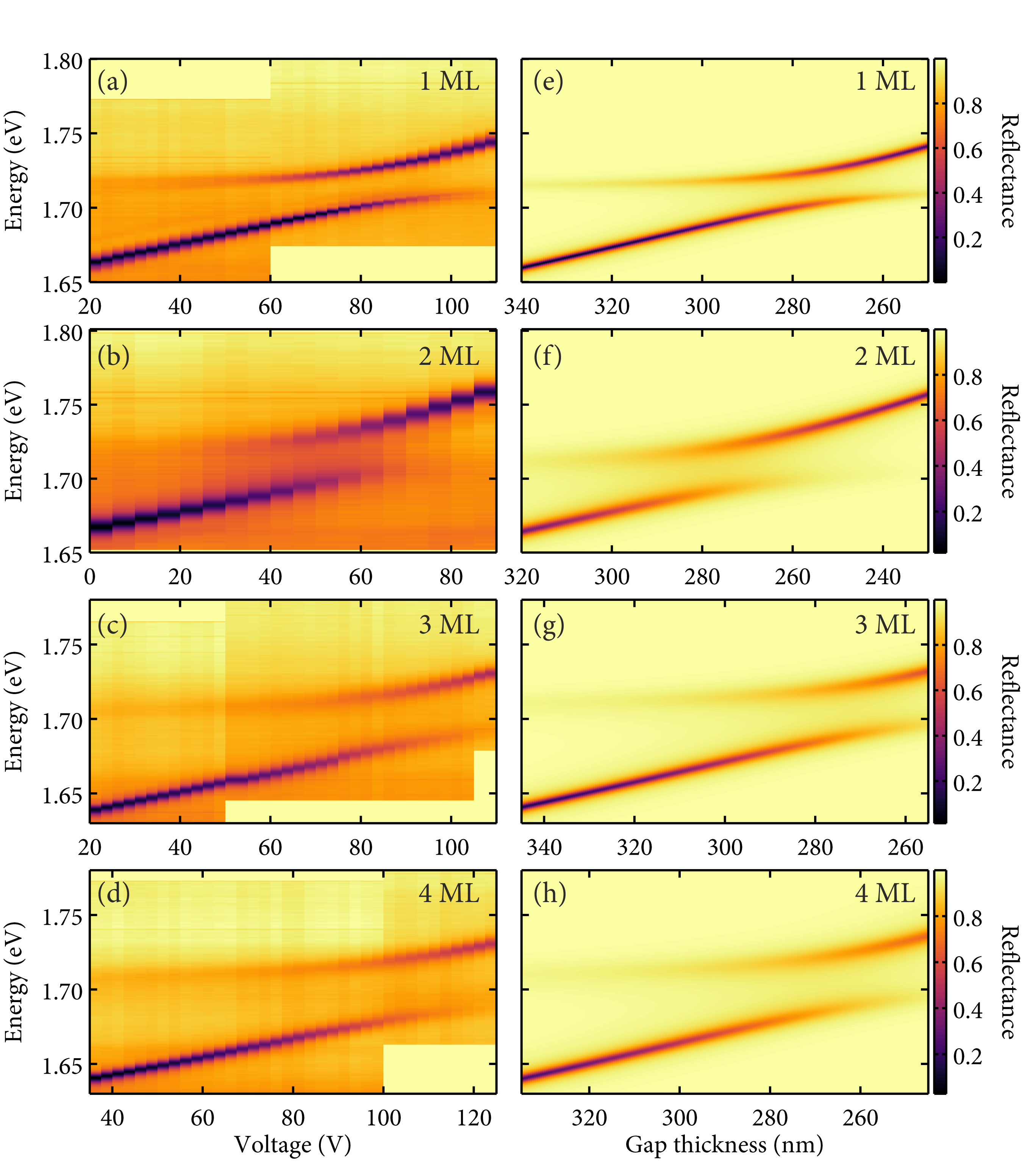
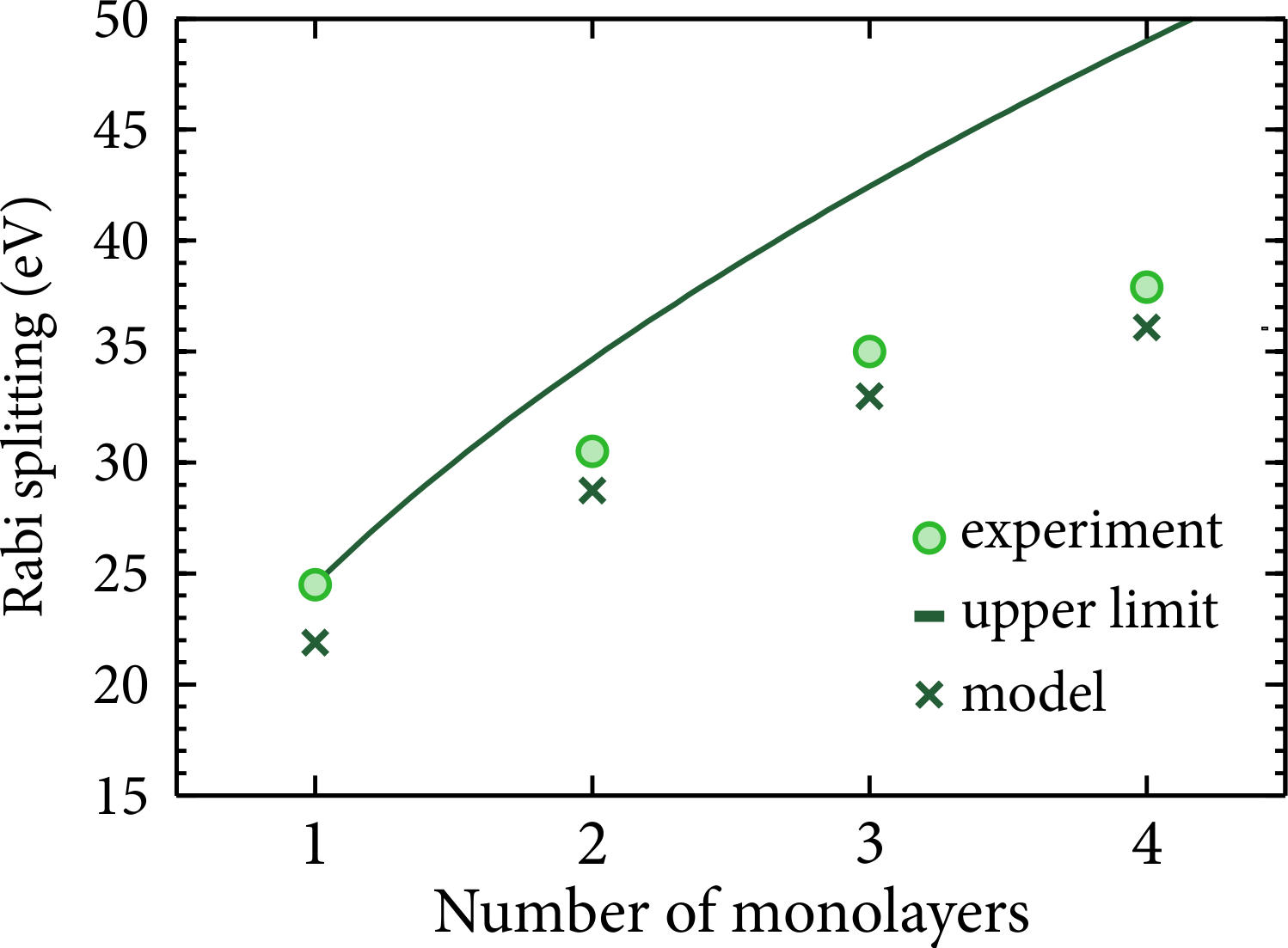
The energy of photons confined in the cavity was tuned in a continuous way by smoothly changing the distance between the mirrors Król et al. (2019). Experimentally, it was realized by placing one of the mirrors on a piezoelectric stage and applying to it an external bias. Reflectance spectra at normal incidence for variable electrical bias applied to the piezoelectric chip taken at the position of a specific WSe2 flake are presented in Fig. 2. Upon applying the voltage, the distance between the DBRs decreases, which results in the increase of the cavity photon energy. When the mode approaches the energy of the excitonic resonance in a given WSe2 flake, a clear anticrossing behaviour can be observed. The minimal energy separation between the modes is equal to the coupling strength , also referred to as the vacuum field Rabi splitting. The observed coupling strength increases with the number of WSe2 layers, as shown in Fig. 3.
The coupling strength between a photonic mode of a planar cavity incorporating an optically active layer with an excitonic resonances can be in general well approximated by Flatten et al. (2016); Savona et al. (1995):
| (1) |
where is the effective cavity length, is the cavity refractive index and is proportional to the exciton oscillator strength in a layer of thickness . The coupling strength given by eq. (1) can provide the upper limit for the Rabi splitting: one can expect an increase of the coupling strength proportional to the square root of the active layer thickness, as plotted with a solid line in Fig. 3. In our experiment we observed a slower increase of the coupling strength with the number of WSe2 layers as compared to that given by the upper limit described above and derived for the monolayer case. Such behaviour can be caused by two factors: change of the exciton resonance width or decrease of the exciton oscillator strength in multilayer WSe2 with respect to the monolayer.
| (eV) | (eV2) | (meV) | (meV) | (meV) | (eV) | (eV2) | (meV) | |||
| 1 ML | 1.7128 | 1.23 | 7.2 | 21.9 | 24.5 | 1.8426 | 0.065 | 4.8 | ||
| 2 ML | 1.7059 | 1.30 | 20.0 | 28.7 | 30.5 | 1.8122 | 0.090 | 20.8 | ||
| 3 ML | 1.7055 | 1.07 | 16.7 | 33.0 | 35.0 | 1.7713 | 0.068 | 15.2 | ||
| 4 ML | 1.7036 | 1.03 | 19.5 | 36.9 | 36.1 | 1.7632 | 0.072 | 19.4 |
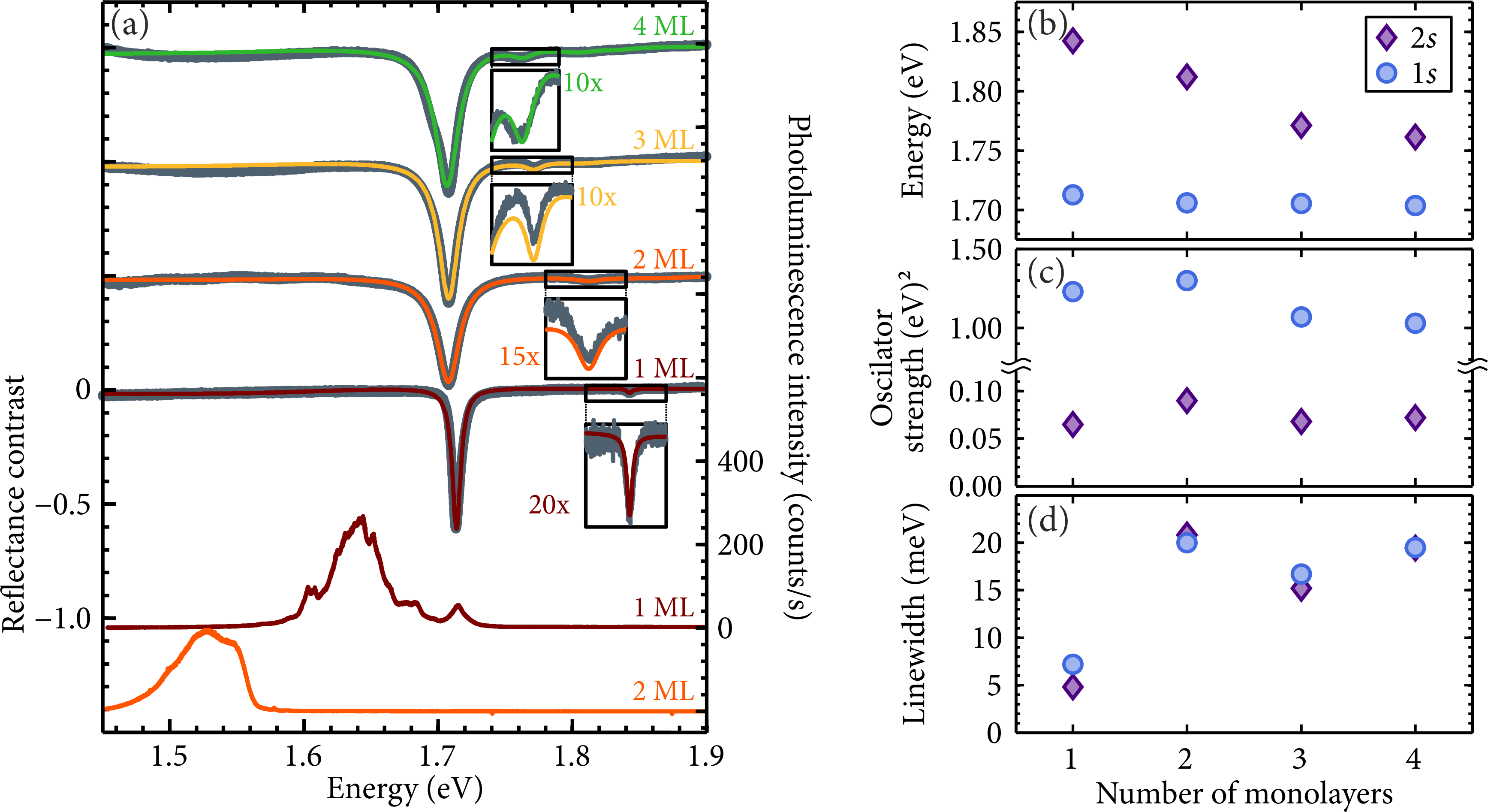
To evaluate the influence of both these factors we performed reflectance contrast (RC) and photoluminescence (PL) measurements without the top DBR. RC spectra taken on each WSe2 flake are presented in Fig. 4. The spectra are dominated by a pronounced dip around 1.71 eV, corresponding to the absorption of a neutral free exciton formed at the valleys, i.e. the so-called A exciton Koperski et al. (2017). For a monolayer, this excitonic transition is also observable in the PL spectrum, which is dominated by a broad band attributed to the so-called localised excitons Arora et al. (2015); Smoleński et al. (2016, 2017); Koperski et al. (2018). With the increase of WSe2 layer thickness, the energy of the excitonic resonance observed in the RC slightly decreases and broadens, with the most significant difference occurring between the monolayer and the bilayer. For WSe2 thicker than the monolayer, as the bandgap changes from direct to indirect, the transitions related to the A excitons can no longer be observed in the PL spectra. For 2 MLs, the emission occurring at around 1.53 eV is related to the indirect bandgap transitions Arora et al. (2015).
The high optical quality of hBN encapsulated flakes allow to observe in RC the first excited exciton states, i.e. 2s Chernikov et al. (2014); He et al. (2014); Chen et al. (2018); Molas et al. (2019), shown in the insets in Fig. 4(a). Their energy separation from the main absorption line significantly decreases with the number of layers due to the expected decrease of the neutral exciton’s binding energy Chernikov et al. (2014).
To extract both the exciton oscillator strength and exciton resonance linewidth, the RC spectra were fitted using a transfer matrix method. The RC signal was calculated based on simulated reflectance of the DBR and the DBR with a corresponding WSe2 layer encapsulated in hBN. The exciton resonance was introduced as a dielectric function of the WSe2 layer given by a Lorentz model in the form provided in Li et al. (2014):
| (2) |
where describes the excitonic ground state and the first excited 2 state. The optical response of the system is also directly dependent on the thicknesses inserted into the transfer matrix model, which makes defined in eq. (2) a measure of the transition strength per unit thickness of a given WSe2 layer. Depending on the number of constituent monolayers, WSe2 the thickness of a given WSe2 flake was taken as a multiple of the single layer thickness equal to 0.65 nm Radisavljevic et al. (2011). The dielectric constant away from the resonances was taken as Li et al. (2014).
The transfer matrix model curves were directly fitted to the experimental RC spectra with , and treated as fitting parameters. The results are presented with solid color lines in Fig. 4. All fitting parameters are also summarised in Tab. 1. Fig. 4(b) shows the energies of excitonic resonances in hBN encapsulated WSe2 flakes of different thicknesses. The ground state energy is almost independent of the layer thickness, whereas the energy of the excited exciton state significantly decreases. For the monolayer, the 2s state is 130 meV above the ground state and for the tetra-layer this energy difference decreases to 61 meV. Also the exciton’s ground state oscillator strength [see Fig. 4(c)] slightly decreases with the number of layers. For the excited exciton states the oscillator strength is 19 to 14 times smaller than for the corresponding ground state with no evident dependence on the number of layers.
It is worth to mention that due to low oscillator strength of the excited 2s exciton state in our samples, we do not observe a strong coupling regime at this transition, as shown in Fig. S9. Such a coupling with excited exciton states has recently become of interest due to large optical nonlinearities one can probe in this type of systems Gu et al. (2019); Walther et al. (2018). In our structures, the 2s exciton-polariton is expected to occur with meV (see Fig. S10), which is much lower than the linewidth of the 2s resonance as shown in Fig. 4(c).
The exciton resonance linewidth determines the optical quality of the layers and is usually affected by homogeneous and inhomogeneous contributions. For both the ground state and the excited 2 state, the spectrally narrowest transition occurs in the monolayer. For the bilayer, the linewidth increases over two times, and then is almost constant for 3- and 4 ML-thick layers. Starting from the 3 ML thick flake, the excitonic resonances reveal a double structure. The appearance of such a fine structure (an increase of the linewidth or a presence of two partially overlapping resonances) can be explained in terms of hybridisation occurring predominantly in the valence band of thicker TMD layers (>1 ML), due to different symmetries of the conduction and valence band orbitals (see Ref. Molas et al. (2017) for details). The analogous effect has already been observed for multilayers of WS2 deposited on Si/SiO2 substrate Molas et al. (2017) and for mono- and few-layer MoS2 encapsulated in hBN Slobodeniuk et al. (2019); Gerber et al. (2019).
The exciton properties obtained from the RC measurements of the WSe2 layers deposited on the DBRs were used to simulate their behaviour inside a full cavity structure, as presented in Fig. 2(e–h). We used the transfer matrix method to simulate the reflectance at normal incidence from a whole structure consisting of two DBRs and a WSe2 flake encapsulated in hBN for variable spacing between the mirrors. The calculations well reproduce the experimental reflectance maps from the left column of Fig. 2. The exciton–photon coupling strength was extracted from the reflectance maps as the minimum energy distance between the two polaritonic branches, and then included in Fig. 3. As can be seen, the simulations slightly underestimate the coupling strength, but properly reconstruct the trend of increasing coupling strength with the thickness of WSe2 layer.
III Summary
In summary, we have demonstrated a strong coupling regime between photons in a planar optical cavity and excitons in multilayer WSe2. We have investigated flakes encapsulated in hBN as well as unprotected ones. The strong coupling is observed regardless of the crossover from direct to indirect bandgap accompanying the transition from the monolayer to -layer thickness. Despite the decrease of the excitons’ oscillator strength per layer thickness at the points of the Brillouin zone in few-layer WSe2, the observed coupling strength increases with the thickness of an active WSe2 layer which proves that multilayers can be well adopted to operate in the strong light-matter coupling regime with substantial absorption at the polariton modes. By changing the number of WSe2 layers and controlling the distance between the Bragg mirrors we were able to tune the energies of the system eigenstates – the exciton-polaritons. Recently, it has been demonstrated that exciton-polaritons in TMDs can be coupled to the emission of a semiconductor quantum well Wurdack et al. (2017); Waldherr et al. (2018), or organic dye Flatten et al. (2017) forming hybrid TMDs-semiconductor-light states. Although indirect transitions analyzed in this paper would decrease the efficiency of such emission, the TMD multilayers should definitely be considered as potential building blocks for future engineering of hybrid TMDs eigenstates.
Methods
Optical measurements
All optical measurements were performed on samples placed in a cryostat at the temperature of 5 K. PL signal was excited nonresonantly with a 514.5 nm (2.41 eV) laser beam. The excitation power, measured before the entrance of a microscope objective, was equal to 100 W and concentrated in approx. 1 m spot. For reflectance and RC measurements a broadband halogen lamp was used with a spot size of approx. 5 m.
Investigations of the cavity structures were performed with angular resolution, achieved by imaging the Fourier space of a high numerical aperture () microscope objective. Data shown in Fig. 2 corresponds to reflectance at normal incidence extracted from the angle-resolved spectra.
Demonstration of strong light-matter coupling regime and formation of the exciton-polariton modes in 1 to 6 ML thick WSe2 flakes, which have not been encapsulated in hBN, can be found in supplementary material.
Acknowledgements
The authors thank Artur Slobodeniuk for helpful discussions. This work has been supported by the Ministry of Higher Education Republic of Poland budget for education via the research projects "Diamentowy Grant" 0109/DIA/2015/44 and 0005/DIA/2016/45; by the National Science Centre: grants 2013/10/M/ST3/00791, 2018/31/B/ST3/02111 and 2018/31/N/ST3/03046; by the EU Graphene Flagship project (ID: 785219), and the ATOMOPTO project (TEAM programme of the Foundation for Polish Science co-financed by the EU within the ERD Fund). B.P. acknowledges Ambassade de France en Pologne for the research stay project. K.W. and T.T. acknowledge support from the Elemental Strategy Initiative conducted by the MEXT, Japan and the CREST (JPMJCR15F3), JST.
References
- Geim and Grigorieva (2013) A. K. Geim and I. V. Grigorieva, “Van der Waals heterostructures,” Nature 499, 419 (2013).
- Mak and Shan (2016) Kin Fai Mak and Jie Shan, “Photonics and optoelectronics of 2D semiconductor transition metal dichalcogenides,” Nat. Photonics 10, 216–226 (2016).
- Britnell et al. (2013) L. Britnell, R. M. Ribeiro, A. Eckmann, R. Jalil, B. D. Belle, A. Mishchenko, Y.-J. Kim, R. V. Gorbachev, T. Georgiou, S. V. Morozov, A. N. Grigorenko, A. K. Geim, C. Casiraghi, A. H. C. Neto, and K. S. Novoselov, “Strong light-matter interactions in heterostructures of atomically thin films,” Science 340, 1311–1314 (2013).
- Koppens et al. (2014) F. H. L. Koppens, T. Mueller, Ph. Avouris, A. C. Ferrari, M. S. Vitiello, and M. Polini, “Photodetectors based on graphene, other two-dimensional materials and hybrid systems,” Nat. Nanotechnol. 9, 780–793 (2014).
- Ahn et al. (2016) Jongtae Ahn, Pyo Jin Jeon, Syed Raza Ali Raza, Atiye Pezeshki, Sung-Wook Min, Do Kyung Hwang, and Seongil Im, “Transition metal dichalcogenide heterojunction PN diode toward ultimate photovoltaic benefits,” 2D Mater. 3, 045011 (2016).
- Pu and Takenobu (2018) Jiang Pu and Taishi Takenobu, “Monolayer transition metal dichalcogenides as light sources,” Adv. Mater. 30, 1707627 (2018).
- Binder et al. (2019) J. Binder, J. Howarth, F. Withers, M. R. Molas, T. Taniguchi, K. Watanabe, C. Faugeras, A. Wysmolek, M. Danovich, V. I. Fal’ko, A. K. Geim, K. S. Novoselov, M. Potemski, and A. Kozikov, “Upconverted electroluminescence via Auger scattering of interlayer excitons in van der Waals heterostructures,” Nat. Commun. 10, 2335 (2019).
- Wang et al. (2018) Gang Wang, Alexey Chernikov, Mikhail M. Glazov, Tony F. Heinz, Xavier Marie, Thierry Amand, and Bernhard Urbaszek, “Colloquium: Excitons in atomically thin transition metal dichalcogenides,” Rev. Mod. Phys. 90, 021001 (2018).
- Koperski et al. (2017) Maciej Koperski, MacIej R. Molas, Ashish Arora, Karol Nogajewski, Artur O. Slobodeniuk, Clement Faugeras, and Marek Potemski, “Optical properties of atomically thin transition metal dichalcogenides: Observations and puzzles,” Nanophotonics 6, 1289–1308 (2017).
- Splendiani et al. (2010) Andrea Splendiani, Liang Sun, Yuanbo Zhang, Tianshu Li, Jonghwan Kim, Chi-Yung Chim, Giulia Galli, and Feng Wang, “Emerging photoluminescence in monolayer ,” Nano Lett. 10, 1271–1275 (2010).
- Mak et al. (2010) Kin Fai Mak, Changgu Lee, James Hone, Jie Shan, and Tony F. Heinz, “Atomically thin : A new direct-gap semiconductor,” Phys. Rev. Lett. 105, 136805 (2010).
- Molas et al. (2017) Maciej R. Molas, Karol Nogajewski, Artur O. Slobodeniuk, Johannes Binder, Miroslav Bartos, and Marek Potemski, “The optical response of monolayer, few-layer and bulk tungsten disulfide,” Nanoscale 9, 13128 (2017).
- Wu et al. (2015) Sanfeng Wu, Sonia Buckley, John R. Schaibley, Liefeng Feng, Jiaqiang Yan, David G. Mandrus, Fariba Hatami, Wang Yao, Jelena Vučković, Arka Majumdar, and Xiaodong Xu, “Monolayer semiconductor nanocavity lasers with ultralow thresholds,” Nature 520, 69–72 (2015).
- Ye et al. (2015) Yu Ye, Zi Jing Wong, Xiufang Lu, Xingjie Ni, Hanyu Zhu, Xianhui Chen, Yuan Wang, and Xiang Zhang, “Monolayer excitonic laser,” Nat. Photonics 9, 733–737 (2015).
- Li et al. (2017) Yongzhuo Li, Jianxing Zhang, Dandan Huang, Hao Sun, Fan Fan, Jiabin Feng, Zhen Wang, and C. Z. Ning, “Room-temperature continuous-wave lasing from monolayer molybdenum ditelluride integrated with a silicon nanobeam cavity,” Nat. Nanotechnol. 12, 987–992 (2017).
- Basov et al. (2016) D. N. Basov, M. M. Fogler, and F. J. García de Abajo, “Polaritons in van der Waals materials,” Science 354, aag1992 (2016).
- Schneider et al. (2018) Christian Schneider, Mikhail M. Glazov, Tobias Korn, Sven Höfling, and Bernhard Urbaszek, “Two-dimensional semiconductors in the regime of strong light-matter coupling,” Nat. Commun. 9, 2695 (2018).
- Kormányos et al. (2015) Andor Kormányos, Guido Burkard, Martin Gmitra, Jaroslav Fabian, Viktor Zólyomi, Neil D Drummond, and Vladimir Fal’ko, “kp theory for two-dimensional transition metal dichalcogenide semiconductors,” 2D Mater. 2, 022001 (2015).
- Liu et al. (2015) Gui-Bin Liu, Di Xiao, Yugui Yao, Xiaodong Xu, and Wang Yao, “Electronic structures and theoretical modelling of two-dimensional group-vib transition metal dichalcogenides,” Chem. Soc. Rev. 44, 2643–2663 (2015).
- Lindlau et al. (2018) Jessica Lindlau, Malte Selig, Andre Neumann, Léo Colombier, Jonathan Förste, Victor Funk, Michael Förg, Jonghwan Kim, Gunnar Berghäuser, Takashi Taniguchi, Kenji Watanabe, Feng Wang, Ermin Malic, and Alexander Högele, “The role of momentum-dark excitons in the elementary optical response of bilayer WSe2,” Nat. Commun. 9, 2586 (2018).
- Li et al. (2018) Yuanzheng Li, Jia Shi, Heyu Chen, Rui Wang, Yang Mi, Cen Zhang, Wenna Du, Shuai Zhang, Zheng Liu, Qing Zhang, Xiaohui Qiu, Haiyang Xu, Weizhen Liu, Yichun Liu, and Xinfeng Liu, “The Auger process in multilayer WSe2 crystals,” Nanoscale 10, 17585–17592 (2018).
- Pudasaini et al. (2018) Pushpa Raj Pudasaini, Akinola Oyedele, Cheng Zhang, Michael G. Stanford, Nicholas Cross, Anthony T. Wong, Anna N. Hoffman, Kai Xiao, Gerd Duscher, David G. Mandrus, Thomas Z. Ward, and Philip D. Rack, “High-performance multilayer WSe2 field-effect transistors with carrier type control,” Nano Research 11, 722–730 (2018).
- Lundt et al. (2016) N Lundt, A Maryński, E Cherotchenko, A Pant, X Fan, S Tongay, G Sęk, A V Kavokin, S Höfling, and C Schneider, “Monolayered MoSe2: a candidate for room temperature polaritonics,” 2D Mater. 4, 015006 (2016).
- Liu et al. (2014) Xiaoze Liu, Tal Galfsky, Zheng Sun, Fengnian Xia, Erh-Chen Lin, Yi-Hsien Lee, Stéphane Kéna-Cohen, and Vinod M. Menon, “Strong light-matter coupling in two-dimensional atomic crystals,” Nat. Photonics 9, 30 (2014).
- Dufferwiel et al. (2018) S. Dufferwiel, T. P. Lyons, D. D. Solnyshkov, A. A. P. Trichet, A. Catanzaro, F. Withers, G. Malpuech, J. M. Smith, K. S. Novoselov, M. S. Skolnick, D. N. Krizhanovskii, and A. I. Tartakovskii, “Valley coherent exciton-polaritons in a monolayer semiconductor,” Nat. Commun. 9, 4797 (2018).
- Flatten et al. (2017) Lucas C. Flatten, David M. Coles, Zhengyu He, David G. Lidzey, Robert A. Taylor, Jamie H. Warner, and Jason M. Smith, “Electrically tunable organic-inorganic hybrid polaritons with monolayer WS2,” Nat. Commun. 8, 14097 (2017).
- Sun et al. (2017) Zheng Sun, Jie Gu, Areg Ghazaryan, Zav Shotan, Christopher R. Considine, Michael Dollar, Biswanath Chakraborty, Xiaoze Liu, Pouyan Ghaemi, Stéphane Kéna-Cohen, and Vinod M. Menon, “Optical control of room-temperature valley polaritons,” Nat. Photonics 11, 491 (2017).
- Waldherr et al. (2018) Max Waldherr, Nils Lundt, Martin Klaas, Simon Betzold, Matthias Wurdack, Vasilij Baumann, Eliezer Estrecho, Anton Nalitov, Evgenia Cherotchenko, Hui Cai, Elena A. Ostrovskaya, Alexey V. Kavokin, Sefaattin Tongay, Sebastian Klembt, Sven Höfling, and Christian Schneider, “Observation of bosonic condensation in a hybrid monolayer MoSe2-GaAs microcavity,” Nat. Commun. 9, 3286 (2018).
- Dufferwiel et al. (2015) S. Dufferwiel, S. Schwarz, F. Withers, A. A. P. Trichet, F. Li, M. Sich, O. Del Pozo-Zamudio, C. Clark, A. Nalitov, D. D. Solnyshkov, G. Malpuech, K. S. Novoselov, J. M. Smith, M. S. Skolnick, D. N. Krizhanovskii, and A. I. Tartakovskii, “Exciton-polaritons in van der Waals heterostructures embedded in tunable microcavities,” Nat. Commun. 6, 8579 (2015).
- Kleemann et al. (2017) Marie-Elena Kleemann, Rohit Chikkaraddy, Evgeny M. Alexeev, Dean Kos, Cloudy Carnegie, Will Deacon, Alex Casalis de Pury, Christoph Große, Bart de Nijs, Jan Mertens, Alexander I. Tartakovskii, and Jeremy J. Baumberg, “Strong-coupling of WSe2 in ultra-compact plasmonic nanocavities at room temperature,” Nat. Commun. 8, 1296 (2017).
- Stührenberg et al. (2018) Michael Stührenberg, Battulga Munkhbat, Denis G. Baranov, Jorge Cuadra, Andrew B. Yankovich, Tomasz J. Antosiewicz, Eva Olsson, and Timur Shegai, “Strong light–matter coupling between plasmons in individual gold bi-pyramids and excitons in mono- and multilayer WSe2,” Nano Lett. 18, 5938–5945 (2018).
- Wang et al. (2019) Shaojun Wang, Quynh Le-Van, Fabio Vaianella, Bjorn Maes, Simone Eizagirre Barker, Rasmus H. Godiksen, Alberto G. Curto, and Jaime Gomez Rivas, “Limits to strong coupling of excitons in multilayer WS2 with collective plasmonic resonances,” ACS Photonics 6, 286–293 (2019).
- Schuller et al. (2013) Jon A. Schuller, Sinan Karaveli, Theanne Schiros, Keliang He, Shyuan Yang, Ioannis Kymissis, Jie Shan, and Rashid Zia, “Orientation of luminescent excitons in layered nanomaterials,” Nat. Nanotechnol. 8, 271 (2013).
- Manca et al. (2017) M. Manca, M. M. Glazov, C. Robert, F. Cadiz, T. Taniguchi, K. Watanabe, E. Courtade, T. Amand, P. Renucci, X. Marie, G. Wang, and B. Urbaszek, “Enabling valley selective exciton scattering in monolayer WSe2 through upconversion,” Nat. Commun. 8, 14927 (2017).
- Cadiz et al. (2017) F. Cadiz, E. Courtade, C. Robert, G. Wang, Y. Shen, H. Cai, T. Taniguchi, K. Watanabe, H. Carrere, D. Lagarde, M. Manca, T. Amand, P. Renucci, S. Tongay, X. Marie, and B. Urbaszek, “Excitonic linewidth approaching the homogeneous limit in -based van der Waals heterostructures,” Phys. Rev. X 7, 021026 (2017).
- Ajayi et al. (2017) Obafunso A Ajayi, Jenny V Ardelean, Gabriella D Shepard, Jue Wang, Abhinandan Antony, Takeshi Taniguchi, Kenji Watanabe, Tony F Heinz, Stefan Strauf, X-Y Zhu, and James C Hone, “Approaching the intrinsic photoluminescence linewidth in transition metal dichalcogenide monolayers,” 2D Mater. 4, 031011 (2017).
- Fang et al. (2019) H. H. Fang, B. Han, C. Robert, M. A. Semina, D. Lagarde, E. Courtade, T. Taniguchi, K. Watanabe, T. Amand, and B. Urbaszek, “Control of the Exciton Radiative Lifetime in van der Waals Heterostructures,” arXiv e-prints , arXiv:1902.00670 (2019), arXiv:1902.00670 [cond-mat.mes-hall] .
- Król et al. (2019) Mateusz Król, Katarzyna Lekenta, Rafał Mirek, Karolina Łempicka, Daniel Stephan, Karol Nogajewski, Maciej R. Molas, Adam Babiński, Marek Potemski, Jacek Szczytko, and Barbara Piętka, “Valley polarization of exciton–polaritons in monolayer WSe2 in a tunable microcavity,” Nanoscale 11, 9574–9579 (2019).
- Flatten et al. (2016) L. C. Flatten, Z. He, D. M. Coles, A. A. P. Trichet, A. W. Powell, R. A. Taylor, J. H. Warner, and J. M. Smith, “Room-temperature exciton-polaritons with two-dimensional WS2,” Sci. Rep. 6, 33134 (2016).
- Savona et al. (1995) V. Savona, L.C. Andreani, P. Schwendimann, and A. Quattropani, “Quantum well excitons in semiconductor microcavities: Unified treatment of weak and strong coupling regimes,” Solid State Commun. 93, 733–739 (1995).
- Arora et al. (2015) Ashish Arora, Maciej Koperski, Karol Nogajewski, Jacques Marcus, Clément Faugeras, and Marek Potemski, “Excitonic resonances in thin films of WSe2: from monolayer to bulk material,” Nanoscale 7, 10421–10429 (2015).
- Smoleński et al. (2016) T. Smoleński, M. Goryca, M. Koperski, C. Faugeras, T. Kazimierczuk, A. Bogucki, K. Nogajewski, P. Kossacki, and M. Potemski, “Tuning valley polarization in a monolayer with a tiny magnetic field,” Phys. Rev. X 6, 021024 (2016).
- Smoleński et al. (2017) T Smoleński, T Kazimierczuk, M Goryca, M R Molas, K Nogajewski, C Faugeras, M Potemski, and P Kossacki, “Magnetic field induced polarization enhancement in monolayers of tungsten dichalcogenides: effects of temperature,” 2D Mater. 5, 015023 (2017).
- Koperski et al. (2018) Maciej Koperski, Maciej R Molas, Ashish Arora, Karol Nogajewski, Miroslav Bartos, Jan Wyzula, Diana Vaclavkova, Piotr Kossacki, and Marek Potemski, “Orbital, spin and valley contributions to zeeman splitting of excitonic resonances in MoSe2, WSe2 and WS2 monolayers,” 2D Mater. 6, 015001 (2018).
- Chernikov et al. (2014) Alexey Chernikov, Timothy C. Berkelbach, Heather M. Hill, Albert Rigosi, Yilei Li, Ozgur Burak Aslan, David R. Reichman, Mark S. Hybertsen, and Tony F. Heinz, “Exciton binding energy and nonhydrogenic rydberg series in monolayer ,” Phys. Rev. Lett. 113, 076802 (2014).
- He et al. (2014) Keliang He, Nardeep Kumar, Liang Zhao, Zefang Wang, Kin Fai Mak, Hui Zhao, and Jie Shan, “Tightly bound excitons in monolayer ,” Phys. Rev. Lett. 113, 026803 (2014).
- Chen et al. (2018) Shao-Yu Chen, Thomas Goldstein, Jiayue Tong, Takashi Taniguchi, Kenji Watanabe, and Jun Yan, “Superior valley polarization and coherence of excitons in monolayer ,” Phys. Rev. Lett. 120, 046402 (2018).
- Molas et al. (2019) M. R. Molas, A. O. Slobodeniuk, K. Nogajewski, M. Bartos, Ł. Bala, A. Babiński, K. Watanabe, T. Taniguchi, C. Faugeras, and M. Potemski, “Energy spectrum of two-dimensional excitons in a nonuniform dielectric medium,” Phys. Rev. Lett. 123, 136801 (2019).
- Li et al. (2014) Yilei Li, Alexey Chernikov, Xian Zhang, Albert Rigosi, Heather M. Hill, Arend M. van der Zande, Daniel A. Chenet, En-Min Shih, James Hone, and Tony F. Heinz, “Measurement of the optical dielectric function of monolayer transition-metal dichalcogenides: , , , and ,” Phys. Rev. B 90, 205422 (2014).
- Radisavljevic et al. (2011) B. Radisavljevic, A. Radenovic, J. Brivio, V. Giacometti, and A. Kis, “Single-layer MoS2 transistors,” Nat. Nanotechnol. 6, 147 (2011).
- Gu et al. (2019) Jie Gu, Lutz Waldecker, Daniel Rhodes, Alexandra Boehmke, Archana Raja, Rian Koots, James C. Hone, Tony F. Heinz, and Vinod M. Menon, “Nonlinear interaction of Rydberg exciton-polaritons in two-dimensional WSe2,” Conference on Lasers and Electro-Optics , FW3M.5 (2019).
- Walther et al. (2018) Valentin Walther, Robert Johne, and Thomas Pohl, “Giant optical nonlinearities from rydberg excitons in semiconductor microcavities,” Nature Commun. 9 (2018), 10.1038/s41467-018-03742-7.
- Slobodeniuk et al. (2019) A O Slobodeniuk, Ł Bala, M Koperski, M R Molas, P Kossacki, K Nogajewski, M Bartos, K Watanabe, T Taniguchi, C Faugeras, and M Potemski, “Fine structure of k-excitons in multilayers of transition metal dichalcogenides,” 2D Mater. 6, 025026 (2019).
- Gerber et al. (2019) Iann C. Gerber, Emmanuel Courtade, Shivangi Shree, Cedric Robert, Takashi Taniguchi, Kenji Watanabe, Andrea Balocchi, Pierre Renucci, Delphine Lagarde, Xavier Marie, and Bernhard Urbaszek, “Interlayer excitons in bilayer with strong oscillator strength up to room temperature,” Phys. Rev. B 99, 035443 (2019).
- Wurdack et al. (2017) Matthias Wurdack, Nils Lundt, Martin Klaas, Vasilij Baumann, Alexey V. Kavokin, Sven Höfling, and Christian Schneider, “Observation of hybrid Tamm-plasmon exciton- polaritons with GaAs quantum wells and a MoSe2 monolayer,” Nat. Commun. 8, 259 (2017).