Substrate effects on charged defects in two-dimensional materials
Abstract
Two-dimensional (2D) materials are strongly affected by the dielectric environment including substrates, making it an important factor in designing materials for quantum and electronic technologies. Yet, first-principles evaluation of charged defect energetics in 2D materials typically do not include substrates due to the high computational cost. We present a general continuum model approach to incorporate substrate effects directly in density-functional theory calculations of charged defects in the 2D material alone. We show that this technique accurately predicts charge defect energies compared to much more expensive explicit substrate calculations, but with the computational expediency of calculating defects in free-standing 2D materials. Using this technique, we rapidly predict the substantial modification of charge transition levels of two defects in MoS and ten defects promising for quantum technologies in hBN, due to SiO and diamond substrates. This establishes a foundation for high-throughput computational screening of new quantum defects in 2D materials that critically accounts for substrate effects.
I Introduction
Point defects such as vacancies and substitutional impurities play a central role in determining the opto-electronic properties of 2D materials desirable for electronic devices and quantum information applications.Toth and Aharonovich (2019); Lin et al. (2016); Wang et al. (2017a); Rasool et al. (2015); Hong et al. (2017); Alkauskas et al. (2016) Their versatile functionality ranges from providing free carriers for charge transport in 2D semiconductorsZhang (2002); Naik and Jain (2018a); Singh et al. (2018) to encoding information in spin states for compact solid-state qubits.Tawfik et al. (2017); Sajid et al. (2018); Gupta et al. (2019); Grosso et al. (2017); Tran et al. (2016) The complexity of controllably synthesizing, identifying and measuring properties of point defects necessitates first-principles computational predictions based on density-functional theory (DFT) to first screen for desirable defects and predict experimental signatures to aid their identification. In 2D materials, calculating energies of charged defects is complicated by the weak and highly anisotropic screening in these systems.Komsa and Pasquarello (2013) The energy of a 2D supercell containing a charged defect diverges with cell size due to strong Coulomb interactions of the defect charge with its periodic images and compensating background.Wang et al. (2015) Several complementary approaches specialized for charged defects in 2D materialsKomsa and Pasquarello (2013); Wang et al. (2015); Sundararaman and Ping (2017) have made it possible to reliably predict charge transition levels and engineer defects in free-standing 2D materials.Wu et al. (2017); Wang et al. (2017b); Freysoldt and Neugebauer (2018); Wang et al. (2017c); Naik and Jain (2018b); Smart et al. (2018); Wang et al. (2019)
However, 2D materials in most experiments and device configurations are not free-standing and are instead deposited, grown or transferred onto a substrate. The substrate is typically an integral part of developing and utilizing 2D materials, critical for nucleation during synthesis and mechanical stability in operation, and it is an unavoidable modification introduced to tune its properties. A thorough understanding of defect properties in 2D materials would therefore be unattainable without taking substrate effects into account. Yet, most computational studies of defects in 2D materials to date ignore substrates primarily due to the extremely high computational cost. Taking the example of monolayer MoS on an SiO substrate here, a typical 66 defect supercell calculation of a free-standing monolayer would require 108 atoms, but including a substrate with a minimal slab of SiO(0001) with six atomic layers increases this to 428 atoms with a 60 increase in computational cost of plane-wave DFT calculations. Repeating such calculations for a large number of substitutional or interstitial impurities with different elements, vacancy configurations and complexes there-of in order to identify ideal defect candidates on specific substrates remains a formidable challenge.
One approach to eliminate this problem would be to remove the substrate atoms from the DFT calculations, and instead approximately capture their effect on the 2D material and defect. Electronic structure calculations in liquid and electrochemical environments have long had to deal with large numbers of environment atoms: practical approaches replace the liquid environment with the response of an appropriately determined dielectric cavity.Tomasi et al. (2005); Marenich et al. (2009); Andreussi et al. (2012) Recent developments of such techniques have facilitated accurate first-principles calculations of complex chemical processes in electrochemical environments, with virtually insignificant computational expense beyond conventional DFT calculations in vacuum.Xiao et al. (2016); Jason D. Goodpaster and Head-Gordon (2016); Sundararaman et al. (2018, 2014); Gunceler et al. (2013); Sundararaman et al. (2015); Sundararaman and Goddard (2015) Analogously, continuum models of substrates could enable rapid computational design of defects in realistic 2D material configurations that include substrates.
In this paper, we present a continuum model approach for capturing substrate effects in DFT calculations of the 2D material alone, which combined with charged defect correction schemes, provides an efficient and general method for evaluating charged defects in realistic 2D material configurations. We benchmark this methodology by predicting ionization energies of Re and Nb substitution defects (Re and Nb) in MoS on substrate SiO (MoS/SiO) and find the lowering of ionization energy due to increased screening from the substrate to be in excellent agreement with DFT calculations that explicitly include the substrate. We then use the so-proven method to predict the transition levels of ten promising defects in hBN on SiO and diamond substrates (hBN/SiO and hBN/Diamond), and show that these defect levels remain deep enough for applications in quantum technologies.
II Theory and Methods
II.1 Charge transition level and Ionization Energy
The formation energy of a defect with charge isZhang and Northrup (1991); Han et al. (2013)
| (1) |
where and are the total energies of the material with and without the defect, involving an exchange of atoms of each species with chemical potential . The electron chemical potential ranges from the valence band maximum to the conduction band minimum .
The calculation of involves a supercell with a net charge, which requires a scheme for correcting the diverging Coulomb interaction energy with periodic images. We employ the model-charge correction scheme described in detail in Refs. 17 and 18. Briefly, this technique corrects the energy and potential of the periodic DFT calculation by comparing Poisson equation solutions for a spherical Gaussian model of the defect charge interacting with a planar model for the anisotropic dielectric response of the material in periodic versus isolated boundary conditions. The anisotropic dielectric function of the 2D material is also calculated from first principles as described in Ref. 18. (See Supplemental Material for details.) We previously showed this technique to be the most robust for 2D materials, requiring no empirical parameters or cell-size extrapolation, and with all quantities extracted purely from DFT calculations of the material.Wu et al. (2017)
Once we can calculate individual charged defect formation energies using this scheme, we can evaluate the charge transition level (CTL) of the defect, defined as the electron chemical potential at which two adjacent charge states and have equal formation energy. Solving for from using (1) yields
| (2) |
For donor defects which transition from to , the transition level relative to the CBM is the donor ionization energy,
| (3) |
while for acceptor defects which transition from to , the transition level relative to the VBM is the acceptor ionization energy,
| (4) |
Substrates strongly influence these ionization energies of defects in 2D materials, and we evaluate these in selected test cases by directly computing of a system containing the 2D material, defect and the substrate. However, such calculations are extremely expensive and we need a technique to account for substrate effects at reduced computational expense.
II.2 Continuum model for substrate effects
The challenge of accounting for a large number of atoms in an environment, analogous to the substrate in the present case, has been addressed extensively using continuum methods for capturing solvent effects in liquid-phase electronic structure calculations.Tomasi et al. (2005); Marenich et al. (2009); Andreussi et al. (2012); Gunceler et al. (2013); Sundararaman et al. (2015); Sundararaman and Goddard (2015) While these continuum solvation techniques vary greatly in details, they share one common aspect: they capture the dominant electrostatic interaction of the environment by placing the ‘solute’ system in a dielectric cavity. The dielectric bound charge induced at the surface of this cavity then approximates the induced charges in the environment atoms, which are now removed from the electronic structure calculation. These models parametrize the cavity, often described in terms of a smooth cavity shape function that goes from 0 in the solute region to 1 in the solvent (environment) region,Gunceler et al. (2013) and constrain parameters by fitting to solvation free energies determined from temperature-dependent solubility measurements.
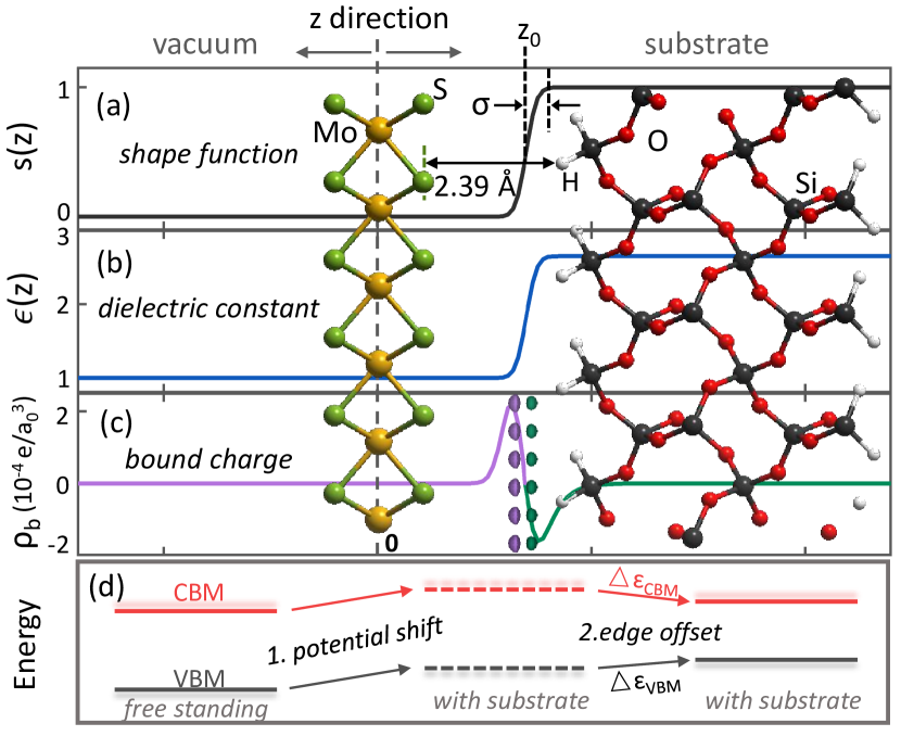
We can similarly replace the dielectric effect of the substrate by replacing it with a dielectric slab described by a smooth shape function (Fig. 1(a)),
| (5) |
which modulates the environment dielectric constant (Fig. 1(b)) as , where is the bulk dielectric constant of the substrate. Note that the appropriate value of the bulk dielectric constant is the optical dielectric constant () if the substrate atoms are not allowed to relax, and the low-frequency value if atomic relaxations are allowed. Here, we used the optical value for all cases, because we do not relax substrate atomic geometry for each defect configuration for computational expediency. In the example of MoS on SiO shown in Fig. 1, the MoS monolayer is centered at , the substrate dielectric function smoothly ‘turns on’ centered at over a width controlled by , to the bulk value of deep within the substrate. (The resulting thicknesses of the vacuum and dielectric slab regions are and respectively, where is the length of the calculation cell normal to the 2D material, as shown in the figure S1 of the Supplemental Material.) Self-consistent solution of the modified Poisson equation with this dielectric profile replaces the Hartree term in the DFT calculation,Gunceler et al. (2013) and produces the bound charge at the surface of the continuum substrate shown in Fig. 1(c).
This substrate continuum model involves as-yet undetermined parameters and which both affect the proximity of the substrate dielectric response to the 2D material. We then constrain the continuum model parameters to reproduce the response of an explicit DFT substrate to charge distributions in the 2D material. First, we calculate the interaction energy of the Gaussian test charge with the DFT substrate,
| (6) |
where and are DFT energies of the substrate alone, with and without an external Gaussian test charge placed at (the center of the 2D material), and is the electrostatic self energy of the Gaussian charge alone. Note that we use the model-charge-based correction scheme to handle the net charge in the supercell calculation of , exactly as for the charged defects.Sundararaman and Ping (2017) Next, for a given dielectric profile based on the cavity shape function , we can directly calculate the interaction energy of the test charge with the continuum dielectric by solving the modified Poisson equation in cylindrical coordinates, which we do using a Bessel function expansion as described in detail in Ref. 17. Finally, we select the cavity parameters such that . However, we have two parameters and , so we fix and determine to satisfy the above condition. (The resulting values of are listed in Table S1 of the Supplemental Material.) Fortunately, we find that the predictions for charged defects are independent of once it is smaller than , as detailed below in the discussion of Fig. 2. In summary, we use two DFT calculations of the substrate alone to determine the continuum model parameters, which can then be used for systematically studying the impact of that substrate on several charged defect configurations in 2D materials.
Beyond the electrostatic interaction of the defect captured by the substrate continuum model, the substrate modifies the electronic band structure of the 2D material itself, which is vital to capture because the defect ionization energies given by (3) and (4) depend on the CBM and VBM energies respectively. Fig. 1(d) summarizes our approach to capture this effect. First, the continuum model accounts for the overall electrostatic potential shift at the location of the 2D material due to the substrate, which shifts the CBM and VBM equally, but does not change the band gap. Next, by aligning core levels (which are sensitive only to electrostatic potential) in density-of-states calculations of the substrate and substrate + perfect 2D material, we can identify the shifts of the VBM and CBM that are beyond electrostatic potential effects. Putting these together, we get the VBM and CBM shifts in the 2D material due to both the overall electrostatic potential and electronic effects beyond it. In the specific example of MoS/SiO shown in Fig. 1(d), we find the offsets to be = +0.056 eV and = -0.008 eV for a net band gap reduction of 0.064 eV due to the SiO substrate. We illustrate this process in greater detail below for hBN on SiO and diamond, including with projected band structures to isolate the 2D material band structure on a substrate. Once again, our overall calculation procedure using the continuum methodology proposed here involves only two calculations of the substrate alone and one of the substrate with a perfect 2D material. Importantly, these calculations are required only once for the 2D material and substrate combination, and no explicit substrates are included in the large supercell calculations per defect configuration.
II.3 Computational details
We implemented the above technique and performed all calculations below in the open-source plane-wave DFT software, JDFTx.Sundararaman et al. (2017) We used the Garrity-Bennett-Rabe-Vanderbilt ultrasoft pseudopotentials at their recommended kinetic energy cutoffs of 20 and 100 Hartrees for the electronic wave function and charge density respectively.Garrity et al. (2014) All supercell calculations below additionally employ Brillouin zone sampling with a 22 Monkhorst-Pack -mesh, and truncated Coulomb interactions to eliminate interactions with periodic images along the slab normal ‘’ direction.Sundararaman and Arias (2013)
We use a 66 supercell with 30 Å and 16 Å lengths in the direction for MoS and hBN respectively, which is sufficient to completely converge results with the truncated Coulomb interactions. (For example, the ionization energy of the C defect in hBN/SiO changes only by 20 meV when this length is increased from 16 Å to 30 Å.) We employ the local-density exchange-correlation functional for the MoS systems in order to benchmark against previous explicit calculations,Noh et al. (2015) and the Perdew-Burke-Ernzerhof generalized gradient functionalPerdew et al. (1996) with DFT-D2 dispersion correctionGrimme (2006) for the hBN systems.
While the technique developed here applies readily to any DFT functional or many-body method, we employed semi-local exchange-correlation functionals to rapidly explore several systems for developing and testing our new method, including with large calculations of explicit substrates. Hybrid DFT and many-body perturbation theory, which typically predict the band edge positions and the gap with greater accuracy,Freysoldt et al. (2009); Hüser et al. (2013) may update the absolute values of ionization energies. In particular, many-body perturbation theory techniques capture more substantial changes in the band edge positions and gap due to substrate screening that is not captured in DFT,Naik and Jain (2018a) which then impacts the ionization energies referenced to the band edges. However, semi-local DFT predicts the correct trends in the defect transition levels, as shown previously for free-standing hBN,Wu et al. (2017); Smart et al. (2018) and we restrict our focus to the DFT level for this initial test of the continuum methods.
For optimal lattice matching, the explicit-substrate MoS/SiO and hBN/SiO calculations respectively used 44 and 33 supercells of -SiO(0001) slabs with six Si atomic layers, while the hBN/Diamond calculations used a 66 supercell of diamond(111) with eight C atomic layers. In each case, the lateral lattice constants were set to the optimal values for the 2D material, resulting in a 5.16%, 0.04% and 0.50% substrate strain in the MoS/SiO, hBN/SiO and hBN/Diamond cases respectively. All dangling bonds on the substrate surfaces were passivated with H atoms. The atomic geometry of the substrate is optimized initially, and then held fixed for the defect supercell calculations for computational efficiency, while the atoms within the 2D material are fully relaxed in all calculations. (Note that this is a convenient benchmark for the continuum model calculations with the substrate dielectric constant set to , as discussed above. The continuum model can be used to predict results corresponding to full relaxation by replacing with the low-frequency dielectric constant at no additional computational cost.)
III Results and Discussion
III.1 Defects in MoS on SiO
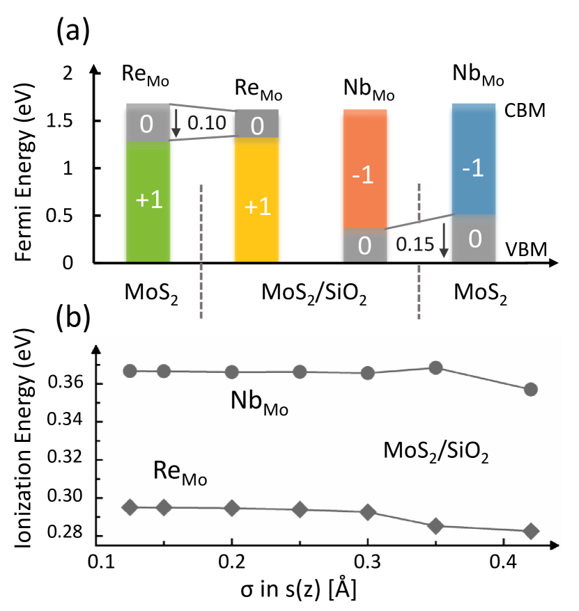
We start by testing our technique on the only charged defects in 2D materials for which previous calculations have explicitly included substrate effects: Re and Nb in MoS/SiO. Re and Nb have one more and less electron relative to Mo, so that these substitution defects act as a donor and an acceptor respectively. Fig. 2(a) shows the prediction of the charge transition level of these defects using the continuum methodology above. Both defects exhibit a reduction of the defect ionization energy by around 0.10-0.15 eV due to the SiO substrate, which is a significant effect for defects that have initial ionization energies of 0.4-0.5 eV. (See Table S2 in the Supplemental Material for a listing of calculated ionization energies.) These continuum model results (in terms of ionization energy reduction) are in excellent agreement of within 0.05 eV with previous results from much more expensive explicit substrate calculations, Noh et al. (2015) demonstrating the reliability of our method. Note that here and below, we present charge transition levels and defect ionization energies instead of the closely related charged defect formation energies because these are easier to standardize and compare across defects; the latter also depend on reference chemical potentials for each atom removed or added by the defect.
Fig. 2(b) shows the variation of the results with the one free parameter that sets the smoothness of the transition from vacuum to substrate dielectric constant. (As discussed above, , which sets the center of the transition of , is constrained using the response of a DFT substrate to a Gaussian test charge, for a given .) The results are insensitive to as long as it is small enough, with variations in the predicted ionization energies far below 0.01 eV for Å. We recommend Å for subsequent calculations, which is small enough to avoid overlap of 2D material charge density with the substrate dielectric response, and yet large enough to exhibit a smooth dielectric constant variation that is easily resolvable on a charge density grid with resolution Å (kinetic energy cutoff Hartrees).
Intuitively, the substrate dielectric screening stabilizes charged states of defects, making them easier to ionize and thereby shifting the charge transition levels closer to the corresponding band edges (VBM for acceptor and CBM for donors). The strong decrease of defect ionization energies in semiconductor MoS is desirable for dopants for 2D electronics, as it makes it possible to introduce charge carriers to the bands at lower temperatures. Yet, the same effect can be undesirable for defect levels sought after for quantum information, where distance from band edges enhances life time of defect excited states, as we discuss next for hBN.
III.2 Defects in hBN on SiO and diamond
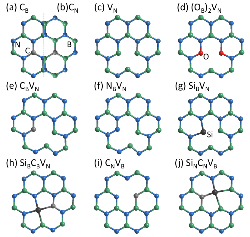
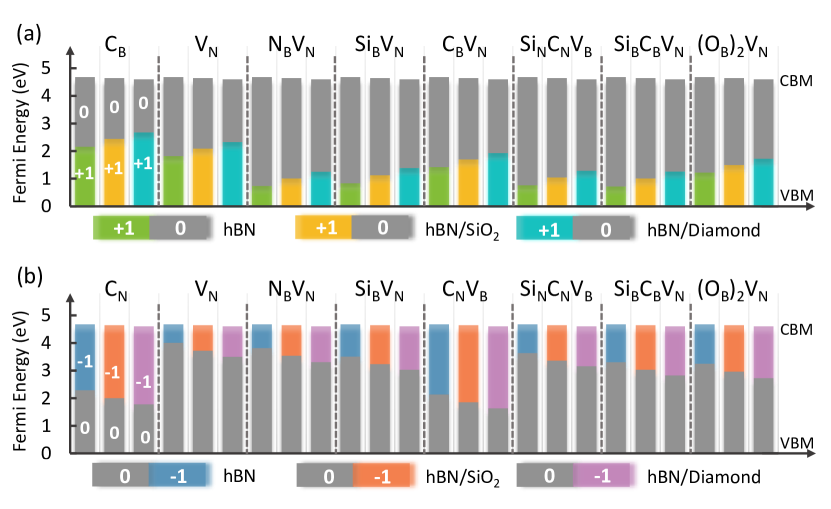
Defects in hBN are the subject of increasing recent interest as candidates for single-photon emission in a 2D analogue of the long-studied nitrogen-vacancy center in diamond. While several recent studies have characterized the properties of spin and charge states in hBN,Wu et al. (2017); Smart et al. (2018); Tawfik et al. (2017); Sajid et al. (2018); Abdi et al. (2018); Reimers et al. (2018) none so far account for the effect of the substrate. We therefore take advantage of the method established above to systematically and rapidly investigate substrate effects on several promising hBN defects, with atomic configurations shown in Fig. 3.
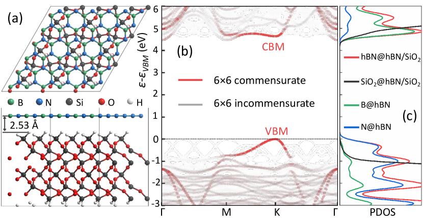
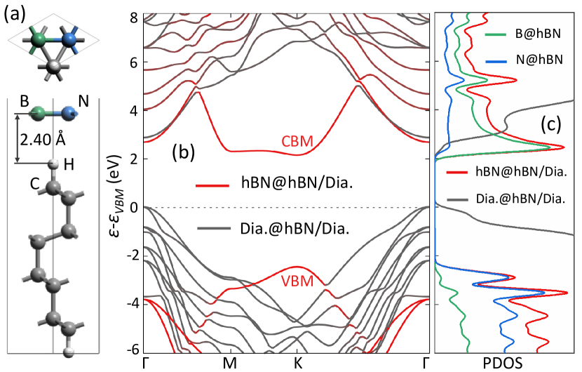
First, we determine the band position changes of hBN, when placed on SiO(0001) and diamond(111) substrates, which is required for ionization energy calculations using (3) and (4). For hBN/SiO, we do this by calculating the density of states (DOS) and unfolding the band structure of the 66 hBN/33 SiO supercell to the Brillouin zone of hBN unit cell.Popescu and Zunger (2012) The unfolding clearly picks out the hBN bands that are commensurate with the unit cell, as shown by the red lines in Fig. 4. The resulting band gap is 4.64 eV, 0.04 eV smaller than in free-standing hBN. On the other hand, hBN and diamond unit cells are already lattice matched within 0.5%, requiring no supercell calculations for determining band alignments. We therefore do not require band structure unfolding in this case, and instead use orbital projections to weight the band structure and identify hBN contributions as shown in Fig. 5. Stronger dielectric screening in diamond reduces the band gap further to 4.60 eV, as shown in Fig. 5(b).
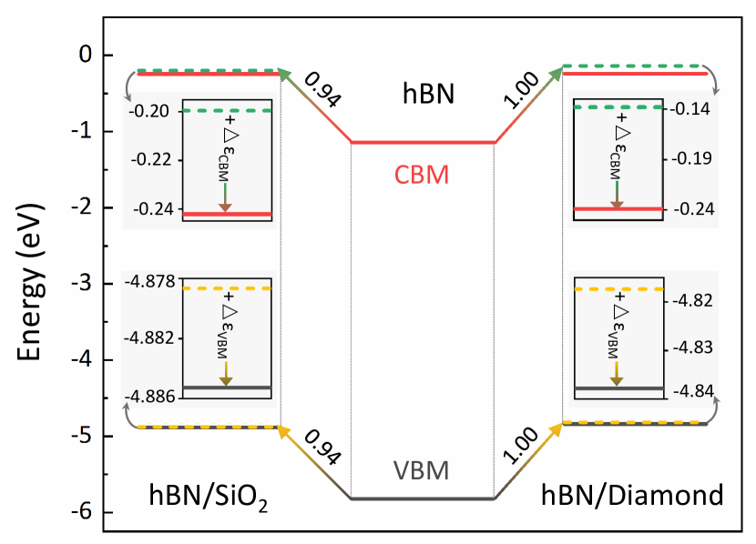
Next, after identifying the band gap modifications, we also need to determine the band edge offsets, and . As discussed above, these offsets consist of an overall electrostatic potential shift due to the substrate that is captured by the solvation model, specifically shifting both VBM and CBM up by 0.94 eV in hBN/SiO and by 1.00 eV in hBN/Diamond relative to free-standing hBN (dashed lines in Fig. 6). Further, by aligning the core levels in the DOS of isolated hBN and hBN with substrates, we can identify the shifts in the VBM and CBM beyond the overall electrostatic potential shift. The band edge offset is not determined from the continuum model and requires explicit DOS calibration. This yields a eV and eV for hBN/SiO, and eV and eV for hBN/Diamond. Adding these offsets yields the final reference band edges for ionization energy calculations within the continuum model (solid lines in Fig. 6).
The total energy calculations using the continuum model along with the band edge positions determined above are now all we need to determine the defect ionization energies, which are the charge transition levels relative to the appropriate band edge. Fig. 7(a) displays the calculated donor ionization energies for several defects in hBN, hBN/SiO and hBN/Diamond, while Fig. 7(b) shows acceptor ionization energies for several defects, all of whose geometries are shown in Fig. 3. Note that many defects are shown in both panels because they can act as both donors and acceptors. The defects are all deep in hBN with ionization energies in the range of 2.14-4.01 eV. Compared to free-standing hBN, ionization energies decrease by 0.27-0.33 eV in hBN/SiO, and 0.47-0.64 eV in hBN/Diamond due to increased dielectric screening by the substrate. However, even with this systematic reduction in ionization energies, all these defect levels remain deep – much larger than thermal and phonon energies in the material – indicating that they are viable to exhibit a long coherence time even after substrate modifications to their energetics.
To confirm the accuracy of these results, we also carried out explicit 2D material + substrate calculations for a few test cases. Specifically, we performed explicit calculations for the C, V and NV donor ionization energies in hBN/SiO, and the donor ionization energies of C and V as well as the acceptor ionization energy of V in hBN/Diamond. We find that our continuum model predictions are accurate to within eV for the hBN/SiO cases, and to within eV for hBN/diamond (see Table S3 in the Supplemental Material for individual values). While the absolute errors are greater than in the MoS case, note that the overall magnitudes of the substrate effects are larger for hBN, resulting in a similar relative accuracy. Similarly, formation energies of neutral defects in hBN/SiO2 and hBN/Diamond from the continuum model are accurate to within eV of the explicit substrate calculations (see Table S4 in the Supplemental Material), with the difference arising mainly from effects beyond the dielectric response such as Pauli repulsion from substrate electrons. Overall, this accuracy is remarkable considering that the continuum model calculations required at most 72 atoms compared to 252 and 432 atoms for hBN/SiO and hBN/Diamond (in addition to just 30 bohrs vacuum size compared to 56.7 and 47.2 bohrs respectively). This amounts to a reduction in computational effort, making it now possible to rapidly explore defect energetics with realistic treatment of substrate effects.
III.3 Ionization energy reduction estimates
| Donors | Self-consistent | Eq. 7 |
|---|---|---|
| (eV) | 0.10 | 0.10 |
| (eV) | 0.32 | |
| (eV) | 0.60 | |
| Acceptors | Continuum Model | Eq. 7 |
| (eV) | 0.15 | 0.14 |
| (eV) | 0.27 | |
| (eV) | 0.48 |
We have so far presented predictions of the ionization energy of several donor and acceptor defects in three 2D material/substrate combinations, and compared against explicit substrate calculations to establish the accuracy of our technique. Table 1 summarizes the reduction in ionization energy from the free-standing 2D material to the 2D material on the substrate in each of these combinations. Note that the reduction in ionization energy is almost the same across all defects within each material/substrate combination.
The reason for this equivalence in ionization energy reduction is that most charged defects have a fairly-localized charge distribution which does not change appreciably upon the introduction of a substrate. The charged defect corrections schemes already take advantage of this fact to remove the periodic interaction between defects by computing the self-energy of a Gaussian model charge in periodic and isolated boundary conditions.Komsa and Pasquarello (2013); Sundararaman and Ping (2017) We could then similarly estimate the reduction in ionization energy of charged defects as the electrostatic stabilization of a Gaussian model charge,
| (7) |
where and are the self energies of the Gaussian model charge in isolated boundary conditions in the dielectric model of the 2D material alone and of the 2D material on the substrate. (These quantities are already used in the charge defect correction for the free-standing 2D material and 2D material on continuum model substrate respectively.) The second term in Eq. 7 accounts for the change in ionization energy due to the substrate-induced shift of the corresponding band edge position, which serves as the reference for defining ionization energies (Eqs. 3 and 4). Note that all quantities in Eq. 7 depend on the 2D material and substrate combination alone, and not on a specific defect.
The final column of Table. 1 shows the results of applying Eq. 7 to each of the three 2D material/substrate combinations studied above. We find that this simple estimate agrees with a typical accuracy of 0.02 eV with the continuum model predictions and a maximum deviation of about 0.04 eV. (See Table S5 in Supplemental Material additionally shows individual results for each defect, compared with this estimate.) This now makes it possible to rapidly estimate the ionization energy of any defect without even performing self-consistent DFT + continuum model calculations of each defect separately. We only need to calculate the ionization energy of all defects of interest in a free-standing 2D material, construct the continuum model for a substrate of interest as described above, and compute a single number using Eq. 7 to shift all free-standing defect ionization energies to the corresponding values on substrates.
IV Conclusions
We have demonstrated a general framework to efficiently and accurately calculate energies and related properties of charged defects in 2D materials on substrates. We resolve the challenge of first-principles evaluation of such systems by treating the substrate as a continuous medium, with its electrostatic response replaced by a continuum dielectric function. Results obtained by this method agree very well with explicit calculations that directly include substrate atoms, but at a small fraction of the computational effort.
This methodology applies to arbitrary combinations of defects, 2D materials and substrates, potentially enabling high-throughput screening of not only defects with unique properties, but also material-substrate combinations targeting desired defect properties. As an example, application of this method to defects in MoS and hBN on SiO and diamond substrates reveals that enhanced screening from surrounding environments can significantly change transition levels. This provides an invaluable input for the experimental identification of 2D defects for quantum information applications such as single photon emission, fully accounting for monolayer 2D materials on realistic substrates, as well as in multilayer 2D materials and 2D heterostructures in future work.
Acknowledgments
We acknowledge startup funding from the Department of Materials Science and Engineering at Rensselaer Polytechnic Institute. All calculations were carried out at the Center for Computational Innovations at Rensselaer Polytechnic Institute.
References
- Toth and Aharonovich (2019) M. Toth and I. Aharonovich, Ann. Rev. Phys. Chem. 70, 123 (2019).
- Lin et al. (2016) Z. Lin, B. R. Carvalho, E. Kahn, R. Lv, R. Rao, H. Terrones, M. A. Pimenta, and M. Terrones, 2D Mater. 3, 022002 (2016).
- Wang et al. (2017a) D. Wang, X.-B. Li, D. Han, W. Q. Tian, and H.-B. Sun, Nano Today 16, 30 (2017a).
- Rasool et al. (2015) H. I. Rasool, C. Ophus, and A. Zettl, Adv. Mater. 27, 5771 (2015).
- Hong et al. (2017) J. Hong, C. Jin, J. Yuan, and Z. Zhang, Adv. Mater. 29, 1606434 (2017).
- Alkauskas et al. (2016) A. Alkauskas, M. D. McCluskey, and C. G. Van de Walle, J. Appl. Phys. 119, 181101 (2016).
- Zhang (2002) S. Zhang, J. Phys.: Cond. Matt. 14, R881 (2002).
- Naik and Jain (2018a) M. H. Naik and M. Jain, Phys. Rev. Mater. 2, 084002 (2018a).
- Singh et al. (2018) A. Singh, A. Manjanath, and A. K. Singh, J. Phys. Chem. C 122, 24475 (2018).
- Tawfik et al. (2017) S. A. Tawfik, S. Ali, M. Fronzi, M. Kianinia, T. T. Tran, C. Stampfl, I. Aharonovich, M. Toth, and M. J. Ford, Nanoscale 9, 13575 (2017).
- Sajid et al. (2018) A. Sajid, J. R. Reimers, and M. J. Ford, Phys. Rev. B 97, 064101 (2018).
- Gupta et al. (2019) S. Gupta, J.-H. Yang, and B. I. Yakobson, Nano Lett. 19, 408 (2019).
- Grosso et al. (2017) G. Grosso, H. Moon, B. Lienhard, S. Ali, D. K. Efetov, M. M. Furchi, P. Jarillo-Herrero, M. J. Ford, I. Aharonovich, and D. Englund, Nature Commun. 8, 705 (2017).
- Tran et al. (2016) T. T. Tran, C. Elbadawi, D. Totonjian, C. J. Lobo, G. Grosso, H. Moon, D. R. Englund, M. J. Ford, I. Aharonovich, and M. Toth, ACS Nano 10, 7331 (2016).
- Komsa and Pasquarello (2013) H.-P. Komsa and A. Pasquarello, Phys. Rev. Lett. 110, 095505 (2013).
- Wang et al. (2015) D. Wang, D. Han, X.-B. Li, S.-Y. Xie, N.-K. Chen, W. Q. Tian, D. West, H.-B. Sun, and S. Zhang, Phys. Rev. Lett. 114, 196801 (2015).
- Sundararaman and Ping (2017) R. Sundararaman and Y. Ping, J. Chem. Phys. 146, 104109 (2017).
- Wu et al. (2017) F. Wu, A. Galatas, R. Sundararaman, D. Rocca, and Y. Ping, Phys. Rev. Mater. 1, 071001 (2017).
- Wang et al. (2017b) D. Wang, D. Han, X.-B. Li, N.-K. Chen, D. West, V. Meunier, S. Zhang, and H.-B. Sun, Phys. Rev. B 96, 155424 (2017b).
- Freysoldt and Neugebauer (2018) C. Freysoldt and J. Neugebauer, Phys. Rev. B 97, 205425 (2018).
- Wang et al. (2017c) D. Wang, X.-B. Li, and H.-B. Sun, Nanoscale 9, 11619 (2017c).
- Naik and Jain (2018b) M. H. Naik and M. Jain, Comput. Phys. Comm. 226, 114 (2018b).
- Smart et al. (2018) T. J. Smart, F. Wu, M. Govoni, and Y. Ping, Phys. Rev. Mater. 2, 124002 (2018).
- Wang et al. (2019) D. Wang, D. Han, D. West, N.-K. Chen, S.-Y. Xie, W. Q. Tian, V. Meunier, S. Zhang, and X.-B. Li, npj Comput. Mater. 5, 8 (2019).
- Tomasi et al. (2005) J. Tomasi, B. Mennucci, and R. Cammi, Chem. Rev. 105, 2999 (2005).
- Marenich et al. (2009) A. V. Marenich, C. J. Cramer, and D. G. Truhlar, J. Phys. Chem. B 113, 6378 (2009).
- Andreussi et al. (2012) O. Andreussi, I. Dabo, and N. Marzari, J. Chem. Phys 136, 064102 (2012).
- Xiao et al. (2016) H. Xiao, T. Cheng, W. A. Goddard III, and R. Sundararaman, J. Am. Chem. Soc. 138, 483 (2016).
- Jason D. Goodpaster and Head-Gordon (2016) A. T. B. Jason D. Goodpaster and M. Head-Gordon, J. Phys. Chem. Lett. 7, 1471 (2016).
- Sundararaman et al. (2018) R. Sundararaman, K. Letchworth-Weaver, and K. A. Schwarz, J. Chem. Phys. 148, 144105 (2018).
- Sundararaman et al. (2014) R. Sundararaman, D. Gunceler, and T. A. Arias, J. Chem. Phys. 141, 134105 (2014).
- Gunceler et al. (2013) D. Gunceler, K. Letchworth-Weaver, R. Sundararaman, K. A. Schwarz, and T. A. Arias, Model. Simul. Mater. Sci. Engi. 21, 074005 (2013).
- Sundararaman et al. (2015) R. Sundararaman, K. A. Schwarz, K. Letchworth-Weaver, and T. A. Arias, J. Chem. Phys. 142, 054102 (2015).
- Sundararaman and Goddard (2015) R. Sundararaman and W. A. Goddard, J. Chem. Phys. 142, 064107 (2015).
- Zhang and Northrup (1991) S. Zhang and J. Northrup, Phys. Rev. Lett. 67, 2339 (1991).
- Han et al. (2013) D. Han, Y. Y. Sun, J. Bang, Y. Y. Zhang, H.-B. Sun, X.-B. Li, and S. B. Zhang, Phys. Rev. B 87, 155206 (2013).
- Sundararaman et al. (2017) R. Sundararaman, K. Letchworth-Weaver, K. A. Schwarz, D. Gunceler, Y. Ozhabes, and T. Arias, SoftwareX 6, 278 (2017).
- Garrity et al. (2014) K. F. Garrity, J. W. Bennett, K. M. Rabe, and D. Vanderbilt, Comput. Mater. Sci. 81, 446 (2014).
- Sundararaman and Arias (2013) R. Sundararaman and T. Arias, Phys. Rev. B 87, 165122 (2013).
- Noh et al. (2015) J.-Y. Noh, H. Kim, M. Park, and Y.-S. Kim, Phys. Rev. B 92, 115431 (2015).
- Perdew et al. (1996) J. P. Perdew, K. Burke, and M. Ernzerhof, Phys. Rev. Lett. 77, 3865 (1996).
- Grimme (2006) S. Grimme, J. Comput. Chem 27, 1787 (2006).
- Freysoldt et al. (2009) C. Freysoldt, P. Rinke, and M. Scheffler, Phys. Rev. Lett. 103, 056803 (2009).
- Hüser et al. (2013) F. Hüser, T. Olsen, and K. S. Thygesen, Phys. Rev. B 87, 235132 (2013).
- Abdi et al. (2018) M. Abdi, J.-P. Chou, A. Gali, and M. B. Plenio, ACS Photonics 5, 1967 (2018).
- Reimers et al. (2018) J. R. Reimers, A. Sajid, R. Kobayashi, and M. J. Ford, J. Chem. Theory Comput. 14, 1602 (2018).
- Popescu and Zunger (2012) V. Popescu and A. Zunger, Phys. Rev. B 85, 085201 (2012).