TCAD model for TeraFET detectors operating in a large dynamic range
Abstract
We present technology computer-aided design (TCAD) models for AlGaAs/InGaAs and AlGaN/GaN and silicon TeraFETs, plasmonic field effect transistors (FETs), for terahertz (THz) detection validated over a wide dynamic range. The modeling results are in good agreement with the experimental data for the AlGaAs/InGaAs heterostructure FETs (HFETs) and, to the low end of the dynamic range, with the analytical theory of the TeraFET detectors. The models incorporate the response saturation effect at high intensities of the THz radiation observed in experiments and reveal the physics of the response saturation associated with different mechanisms for different material systems. These mechanisms include the gate leakage, the velocity saturation and the avalanche effect.
Index Terms:
TeraFET, terahertz detection, modeling, TCAD, HFET, MOSFETI Introduction
The TeraFETs, plasmonic field effect transistors (FETs) applied in the terahertz (THz) frequency range, have been proposed since the early 1990s [1, 2, 3]. Over decades they have found wide applications in THz mixers [4, 5], frequency multipliers [6, 7], transceivers [8, 9], imagers and sensors [10, 11, 12], etc. Recent interests include operating TeraFET detectors at high incident power, which could be used to measure the duration and structure of the high-power THz pulses [13]. At large intensities of the incident THz radiation, the response has been observed to saturate in the measurements [14]. Different propositions have been made to explain this effect [15, 16, 17]. In this work we explore the reason for the response saturation effect by examining different physical mechanisms in the physics-based simulations using the validated TCAD models [18]. The results reveal the physics of the response saturation associated with different mechanisms for different material systems. These mechanisms include the leakage current, the velocity saturation, and the avalanche effect. This insight into the device physics allows for the development of the next generation compact models for the TeraFET detectors that are valid over a wide dynamic operation range.
II THz TCAD Models
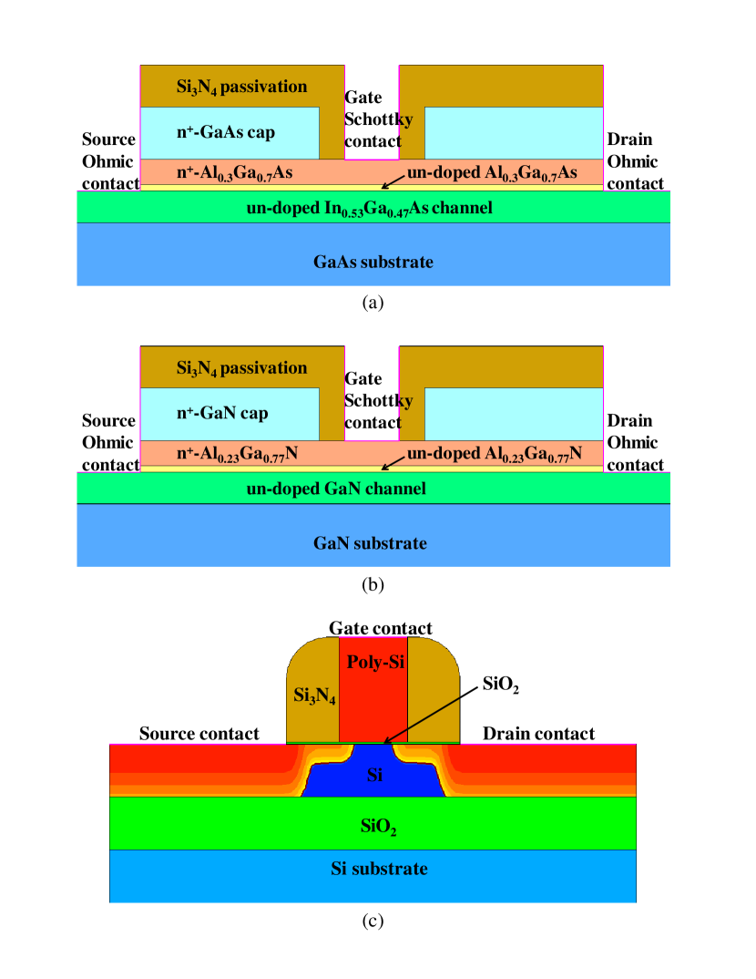
Fig. 1 shows the structures of the TeraFETs for different material systems in Synopsys Sentaurus TCAD. The TCAD models account for the hydrodynamic transport suitable for deep-submicron and heterostructure devices, and the velocity saturation, the generation-recombination, and the barrier tunneling mechanisms [19].
II-A AlGaAs/InGaAs HFETs
The AlGaAs/InGaAs HFET TCAD model was built to simulate the 130 nm AlGaAs/InGaAs pHEMTs fabricated by TriQuint Inc. (now Qorvo) [20]. It has been validated by comparing the simulated I-V characteristics and the dependence of the THz response on the gate bias with the measured data and the analytical results [18].
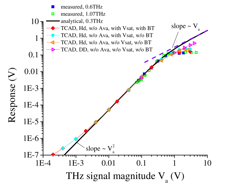
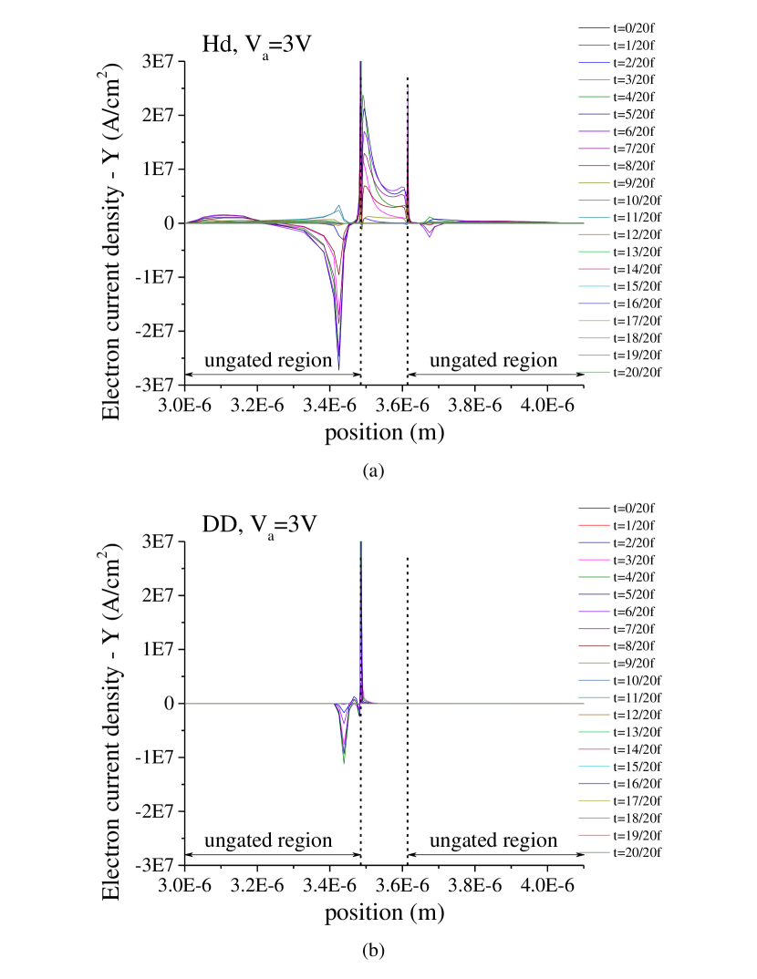
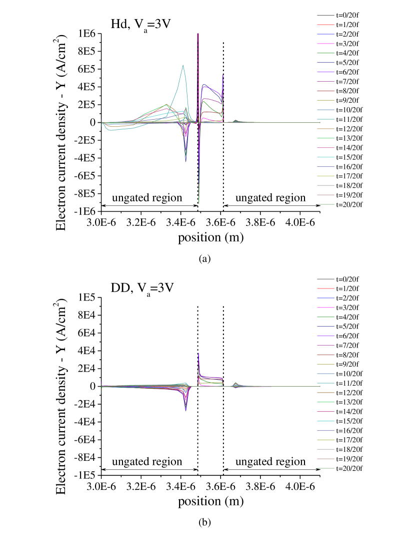
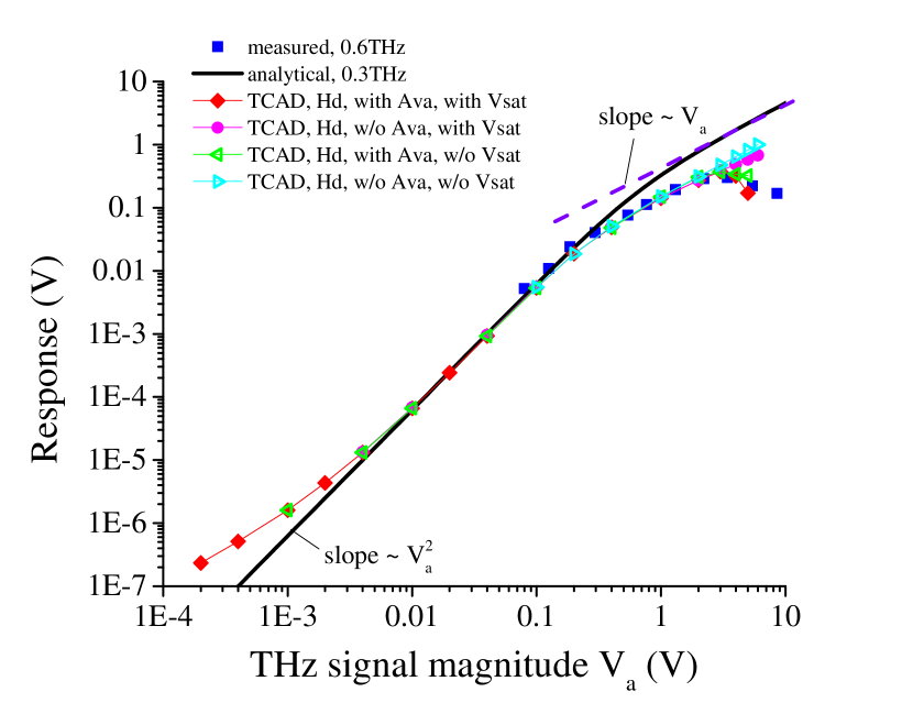
Fig. 2 shows the dependence of the simulated detector response at 0.3 THz above threshold ( 0.12 V) on the THz signal magnitude for the AlGaAs/InGaAs HFET TCAD model, compared with the measured data in [14] and the analytical results with the open boundary condition at the drain. To explore the device physics for the response saturation, different physical mechanisms including the hydrodynamic (Hd) or drift-diffusion (DD) transport, avalanche (Ava), velocity saturation (Vsat), and gate barrier tunneling (BT) were turned on and off in the simulation. It could be seen that the simulated response gives a quadratic response (proportional to ) at low intensities, which is consistent with the analytical result from around 5 mV to 1 V. At high intensities ( 1 V), the response saturation observed in the measurements could also be demonstrated in the TCAD model, but not in the analytical result, since the analytical theory uses the next terms in the Taylor series expansion of the response dependence on the THz voltage [21]. Hence, the analytical theory applies to an intermediate range of powers but it cannot reproduce the entire dynamic range. Also, the model with the drift-diffusion transport does not show the response saturation effect at high intensities of the incident THz radiation ( 1 V), while the models with the hydrodynamic transport show the response saturation behavior. The main difference between the hydrodynamic transport and the drift-diffusion transport in TCAD is that the hydrodynamic model accounts for the energy transport across heterointerfaces, which is not considered in the drift-diffusion model. Therefore, the hydrodynamic transport could lead to larger gate leakage than the drift-diffusion transport. Hence, the response saturation could be associated with the gate leakage which contributes to the rectification of the input THz signal at the gate. Fig. 3 shows the profiles of the electron current density transverse to the conducting channel direction at the positions closely (1 nm) below the Schottky gate contact at different times within a period for 3 V using the hydrodynamic and drift-diffusion models. As seen, the profiles with the hydrodynamic transport show much larger gate leakage current than the drift-diffusion transport.
II-B AlGaN/GaN HFETs
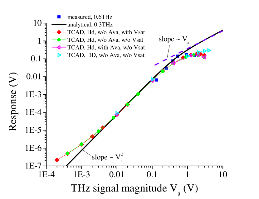
The TCAD model developed for the AlGaN/GaN HFET uses the same dimensions with the AlGaAs/InGaAs HFET TCAD model, as shown in Fig. 1 (b). Fig. 4 shows the simulated detector response at 0.3 THz above threshold ( 0.12 V) as a function of the THz signal magnitude for the AlGaN/GaN HFET TCAD model with different physical mechanisms, compared with the measured data in [14] and the analytical results with the open boundary condition at the drain. Again, from the profiles of the electron current density transverse to the channel at the positions closely (1 nm) below the Schottky gate contact in Fig. 5, the response saturation could be linked to the higher gate leakage current observed in the hydrodynamic transport than in the drift-diffusion transport.
II-C Si MOSFETs
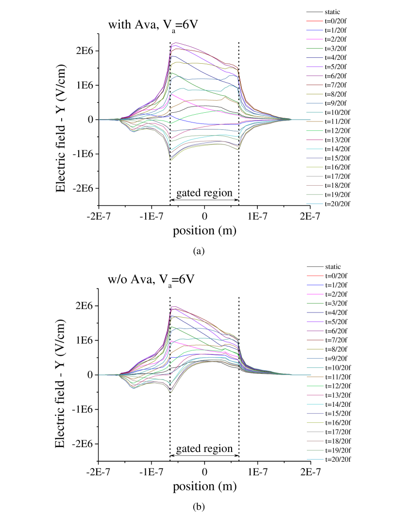
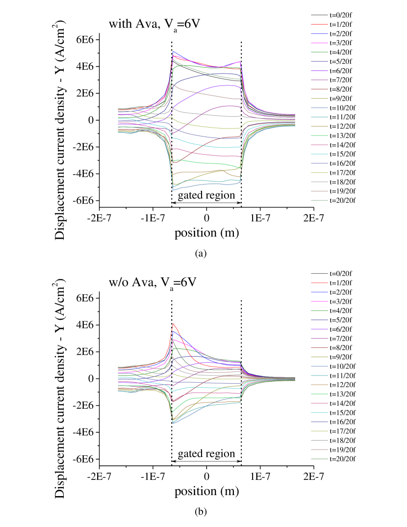
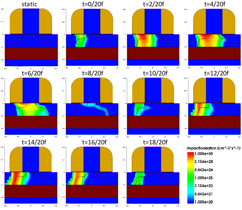
The response saturation at high intensities of the THz radiation was also observed for Si MOSFETs [14]. Since the gate leakage could be negligible in Si MOSFETs due to the gate insulator, other mechanisms could be responsible for the response saturation. To investigate this, the TCAD model in Fig. 1 (c) is considered. The model is set up based on an exemplary silicon-on-insulator (SOI) N-channel MOSFET using the default material parameter files for silicon in Sentaurus TCAD [19]. The gate length for the model is set as 130 nm, the same as for the HFET models. The response saturation could also be demonstrated at large intensities with the SOI MOSFET TCAD model, as shown in Fig. 6. The comparison of the simulated results with different mechanisms shows that the response saturation could be associated with the avalanche effect and also affected by the velocity saturation. The electric field in the gate oxide was checked to be below the SiO2 breakdown field (10 MV/cm) indicating no gate breakdown. However, at high THz fields, carriers could be generated from impact ionization and travel into the channel and change the electric field which could affect the response at the drain. This effect of the avalanche model could be seen in Fig. 7 which shows the profiles of the electric field transverse to the channel at the positions along the channel and closely (1 nm) below the SiO2/Si interface within a period above threshold ( 0.2 V). Also, although the gate conduction current is zero, the displacement current at the gate exists, as shown in Fig. 8. The inclusion of the avalanche model leads to higher displacement current near the drain, which could play a similar role as the gate leakage in the HFETs. Fig. 9 shows the profiles of the impact ionization rate at 6 V at different times within a period for the SOI MOSFET TCAD model with the avalanche effect, indicating where the carriers could be generated at high intensities of the incident THz radiation.
III Conclusion
In this work, the TCAD models valid in a large dynamic range were presented. The TCAD models explain the experimentally observed response saturation at high intensity levels of the incident THz radiation (above 1 V). By activating or deactivating different physical mechanisms in the TCAD models, the reason for the response saturation effect was found out to be associated with the gate leakage for AlGaAs/InGaAs HFETs and AlGaN/GaN HFETs and affected by the velocity saturation and the avalanche effect for Si MOSFETs.
References
- [1] M. Dyakonov and M. S. Shur, “Shallow water analogy for a ballistic field effect transistor: New mechanism of plasma wave generation by dc current,” Phys. Rev. Lett., vol. 71, no. 15, pp. 2465–2468, Oct. 1993.
- [2] M. I. Dyakonov and M. S. Shur, “Detection, mixing, and frequency multiplication of terahertz radiation by two-dimensional electronic fluid,” IEEE Trans. Electron Devices, vol. 43, no. 3, pp. 380–387, Mar. 1996.
- [3] M. I. Dyakonov and M. S. Shur, “Plasma wave electronics: novel terahertz devices using two-dimensional electron fluid,” IEEE Trans. Electron Devices, vol. 43, no. 10, pp. 1640–1645, Oct. 1996.
- [4] H. Marinchio et al., “Room-temperature terahertz mixer based on the simultaneous electronic and optical excitations of plasma waves in a field effect transistor,” Appl. Phys. Lett., vol. 96, no. 1, pp. 013502, Jan. 2010.
- [5] S. Preu et al., “Terahertz detection by a homodyne field effect transistor multiplicative mixer,” IEEE Trans. Terahertz Sci. Technol., vol. 2, no. 3, pp. 278–283, May 2012.
- [6] K. Wu, S. Muralidharan, and M. M. Hella, “A Wideband SiGe BiCMOS Frequency Doubler with 6.5-dBm Peak Output Power for Millimeter-Wave Signal Sources,” IEEE Trans. Microw. Theory Tech., vol. 86, no. 3, pp. 187–200, Jan. 2018.
- [7] S. Muralidharan, K. Wu, and M. Hella, “A 165-230GHz SiGe amplifier-doubler chain with 5dBm peak output power,” in IEEE RFIC Symposium, San Francisco, CA, USA, 2016, pp. 302–305.
- [8] S. Muralidharan, K. Wu, and M. Hella, “A 216GHz 0.5 mW transmitter with a compact power combiner in 65nm CMOS,” in Microwave Conference (APMC), 2015 Asia-Pacific, vol. 2, pp. 1–3, Dec. 2015.
- [9] K. Wu, B. Fahs, and M. Hella, “A 220 GHz OOK Outphasing Transmitter in 130-nm BiCMOS Technology,” 2018 IEEE BiCMOS and Compound Semiconductor Integrated Circuits and Technology Symposium (BCICTS), pp. 227–230, Oct. 2018.
- [10] W. Knap et al., “Field effect transistors for terahertz detection: Physics and first imaging applications,” J. Infrared Millim. Terahertz Waves, vol. 30, no. 12, pp. 1319–1337, Dec. 2009.
- [11] A. Lisauskas et al., “Exploration of terahertz imaging with silicon MOSFETs,” J. Infrared Millim. Terahertz Waves, vol. 35, no. 1, pp. 63–80, Jan. 2014.
- [12] N. Dyakonova et al., “Terahertz vision using field effect transistors detectors arrays,” in 2018 22nd International Microwave and Radar Conference (MIKON), pp. 711–714, May 2018.
- [13] S. Preu, M. Mittendorff, S. Winnerl, O. Cojocari, and A. Penirschke, “THz autocorrelators for ps pulse characterization based on Schottky diodes and rectifying field-effect transistors,” IEEE Trans. Terahertz Sci. Technol., vol. 5, no. 6, pp. 922–929, Nov. 2015.
- [14] D. B. But et al., “The dynamic range of THz broadband FET detectors,” in Proc. SPIE, Terahertz Emitters, Receivers, and Applications IV, San Diego, CA, USA, Sep. 2013, vol. 8846, Art. no. 884612.
- [15] D. B. But et al., “Nonlinear photoresponse of field effect transistors terahertz detectors at high irradiation intensities,” J. Appl. Phys., vol. 115, no. 16, Apr. 2014, Art. no. 164514.
- [16] N. Dyakonova et al., “Saturation of photoresponse to intense THz radiation in AlGaN/GaN HEMT detector,” J. Appl. Phys., vol. 120, no. 16, Oct. 2016, Art. no. 164507.
- [17] N. Dyakonova et al., “AlGaN/GaN HEMT’s photoresponse to high intensity THz radiation,” Opto-Electron. Rev., vol. 23, no. 3, pp. 195–199, Sep. 2015.
- [18] X. Liu and M. Shur, “An efficient TCAD model for TeraFET detectors,” in 2019 IEEE Radio and Wirel. Symp. (RWS), Orlando, FL, USA, Jan. 2019, to be published.
- [19] Sentaurus Device User Guide (Version N-2017.09), Synopsys Inc., Mountain View, CA, USA, 2017.
- [20] A. T. Ping, W. Liebl, G. Mahoney, S. Mahon, and O. Berger, “A High-Performance 0.13-µm AlGaAs/InGaAs pHEMT Process Using Sidewall Spacer Technology,” in 2005 GaAs MANTECH Dig., Apr. 2005.
- [21] A. Gutin, V. Kachorovskii, A. Muraviev, and M. Shur, “Plasmonic terahertz detector response at high intensities,” J. Appl. Phys., vol. 112, no. 1, Jul. 2012, Art. no. 014508.