Electric selective activation of memristive interfaces in TaOx-based devices
Abstract
The development of novel devices for neuromorphic computing and non-traditional logic operations largely relies on the fabrication of well controlled memristive systems with functionalities beyond standard bipolar behavior and digital ON-OFF states. In the present work we demonstrate for Ta2O5-based devices that it is possible to selectively activate/deactivate two series memristive interfaces in order to obtain clockwise or counter-clockwise multilevel squared remanent resistance loops, just by controlling the (a)symmetry of the applied stimuli and independently of the nature of the used metallic electrodes. Based on our thorough characterization, analysis and modeling, we show that the physical origin of this electrical behavior relies on controlled oxygen vacancies electromigration between three different zones of the active Ta2O5-x layer: a central -bulk- one and two quasi-symmetric interfaces with reduced TaO2-h(y) layers. Our devices fabrication process is rather simple as it implies the room temperature deposition of only one CMOS compatible oxide -Ta-oxide- and one metal, suggesting that it might be possible to take advantage of these properties at low cost and with easy scability. The tunable opposite remanent resistance loops circulations with multiple -analogic- intermediate stable states allows mimicking the adaptable synaptic weight of biological systems and presents potential for non-standard logic devices.
I Introduction
Non-volatile resistive switching (RS) devices, usually called memristors, are intensively studied due to their potential as resistive random access memories (ReRAM) Ielmini and Waser (2016), novel logic units Borghetti et al. (2010) and neuromorphic computing Yu (2017) devices. RS has been found for a large number of simple and complex transition metal oxides, including TaOx Prakash et al. (2013). Outstanding memristive figures have been reported in this system, including endurances larger than 1012 cycles Lee et al. (2011), ON-OFF ratios up to 106 and retention times greater than 10 years Shi et al. (2017). RS in simple oxides such as TaOx has been reported as bipolar and the physical mechanism was usually attributed to the creation and disruption of conducting oxygen vacancies (OV) nano-filaments Prakash et al. (2013). This process usually takes place in a region close to a metal electrode with a high work function such as Pt, which in contact with a n-type insulating oxide forms a Schottky barrier Baek et al. (2016). The drift diffusion of OV to and from the interface under the action of the external electrical field modifies the Schottky barrier and modulates its resistance. The application of negative voltage to the electrode attracts positively charged OV to the interface and triggers the transition from high resistance (HR) to low resistance (LR), usually called SET process. The opposite transition is achieved with positive voltage and is usually called RESET process. In this way, the circulation of the current-voltage (I-V) curve is clockwise in the positive current-positive voltage quadrant, while the remanent resistance vs. voltage curve (usually called Hysteresis Switching Loop, HSL Rozenberg et al. (2010)) displays a counter-clockwise behavior.
The possibility of opposite (counter-clockwise) I-V and (clockwise) HSL circulations was also shown for TiO2/Pt interfaces, and attributed to oxygen exchange between Pt and TiO2 at the local position of the filament Zhang et al. (2018). Opposite switching polarities were also reported for TaOx devices and attributed to a competition between ionic motion and electronic - i.e charge trapping- effects La Torre et al. (2017), to the formation of filaments with either conical or hour-glass shapes Park et al. (2015, 2017) or to volumetric oxygen vacancies exchange between TaOx layers with different stochiometries Yang et al. (2012). The coexistance of two bipolar memristive regimes with opposite polarities in a single device allows to increase or decrease the resistance of the device with stimulus of different amplitudes but the same polarity, which has potential for the development of beyond von Neumann novel computing devices Zhang et al. (2018).
Asymmetric devices (i.e. an insulating oxide sandwiched between two electrodes of different metals) with an active interface and an ohmic non-active one were reported to display squared HSL Ghenzi et al. (2013, 2014). On the contrary, symmetric systems presenting two similar metal/oxide memristive active interfaces in series were reported to display HSLs with the so-called “table with legs” (TWL) shape Chen et al. (2005); Rozenberg et al. (2010). In these cases, the two interfaces behave in a complementary way: when one switches from low resistance (LR) to high resistance (HR), the other switches inversely. Symmetric Pt/TiO2/Pt devices stimulated with symmetric stimuli displayed complex I-V curves with multiple transitions, which was interpreted as bipolar switching taking place simultaneously at both Pt/TiO2 interfaces Jeong et al. (2009).
In the present paper we show for Ta2O5-based devices that a careful tuning of the stimuli protocol allows to selectively activate/deactivate the contribution of two memristive interfaces to the overall RS behavior, allowing to obtain both clockwise/counter-clockwise multilevel squared HSL or a “table with legs” behavior, where both interfaces are active simultaneously.
We show that the (a)symmetry of the electrical response can be controlled by appropriately tuning the electroforming process and the subsequent excitation protocol, independently of the electrodes symmetry. From a combination of I-V curves analysis and modeling, togheter with numerical simulations based on the Voltage Enhanced Oxygen Vacancy migration (VEOV) model Rozenberg et al. (2010), adapted for binary oxides-based devices Ghenzi et al. (2013), we achieve a thorough understanding of the observed phenomenology, which is rationalized in terms of oxygen vacancies electromigration between a central (bulk) zone of the active Ta2O5 layer and its interfaces with metallic TaOx (x 2). Finally, the potential technological implications of the observed tunable opposite HSL circulations with multiple intermediate stable states are discussed.
II Results
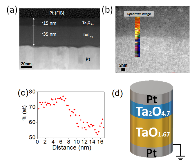
We have fabricated and characterized Ta-oxide bilayers grown on platinized silicon at different oxygen pressures. We will first describe the performed transmission electron microscopy characterization. Figure 1(a) shows a STEM-HAADF cross section, evidencing that the thicknesses of the Ta-oxide layers grown at 0.01 (layer B) and 0.1 (layer A) mbar of O2 are 35nm and 15nm, respectively. Both layers are amorphous and differ in their contrast. A brighter image is found for the B layer, indicating a higher relative concentration of Ta (see the blow up displayed in Figure S1 of the Supp. Information), consistently with a more reduced oxide and the lower oxygen pressure used for its growth. Figure 1(b) shows an STEEM-HAADF-EELS map of the bilayer indicating a higher relative concentration of oxygen at the top A layer. Performed quantifications, as the one shown in Figure1 (c), indicate average oxygen concentrations of %at and 60%at for A and B layers, respectively. This suggests average stochiometries for A and B layers of Ta2O4.70 and TaO1.67, indicating in the latter case a mixture of 67 % TaO2 and 33 % TaO. Consistent results are obtained from STEEM-HAADF-EDX quantification, as shown in Figure S1 of the Supp. Information si .
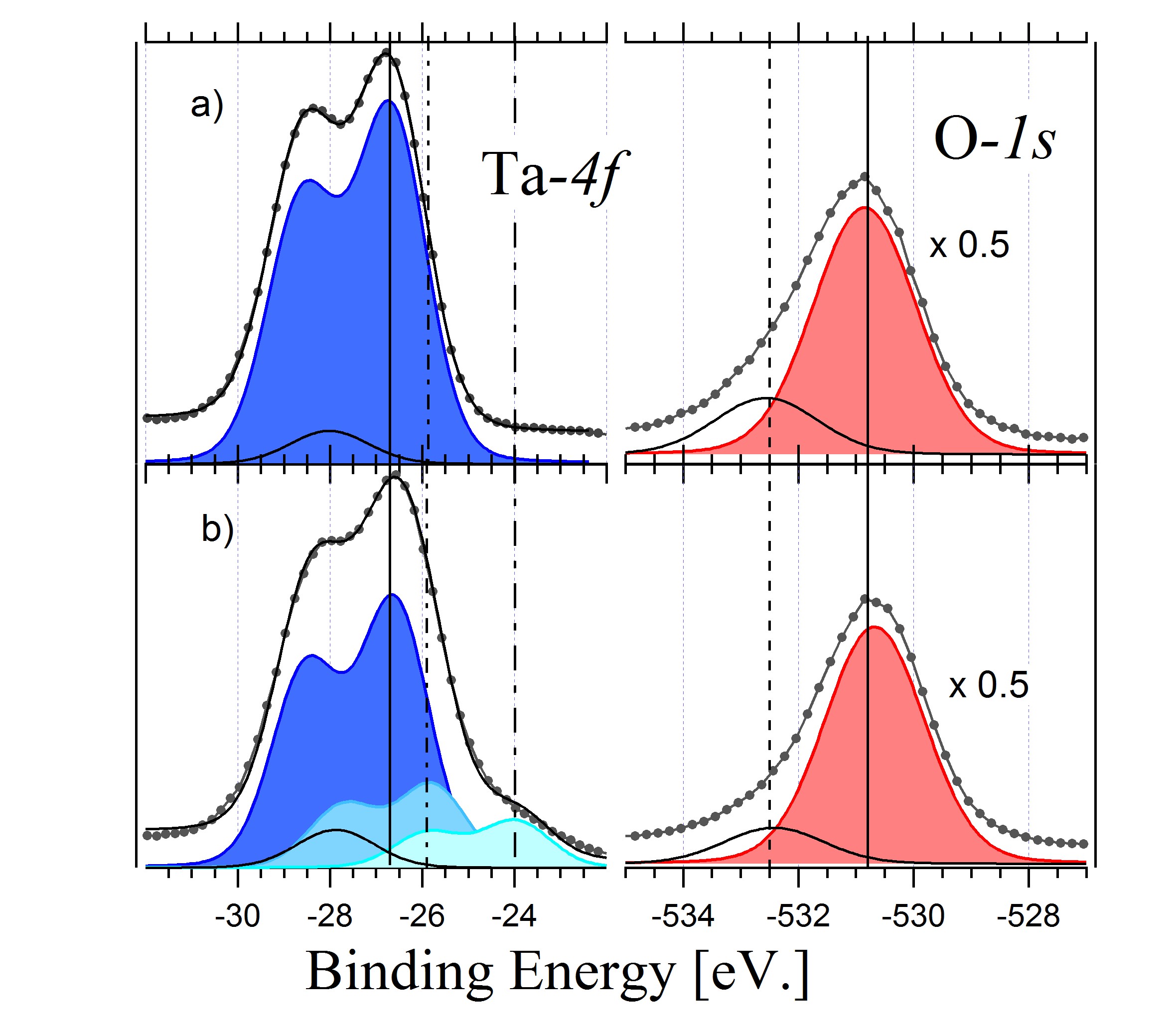
XPS measurements were performed to obtain information of the films surface chemical composition and Ta oxidation states. Both Ta- and O- spectra are shown in Figure 2 (a) and (b) for TaOx films grown at 0.1 mbar and 0.01 mbar of O2, respectively. The spectra were fitted using a Voight function for each peak plus a Shirley-type background. The total fitted intensities along with the experimental ones are shown in each spectrum. Ta-4f spectra components are characerized by two identical peaks corresponding to the spin-orbit split between 4f7/2 and 4f5/2 levels, with relative intensities of 3:4. The Ta-4f spectrum of the film grown at 0.1mbar of O2 display one component corresponding to Ta2O5 and for the film grown at 0.01mbar of O2 three components were identified: a major one at binding energy 26.7 eV ascribed to Ta2O5 and two minor ones at binding energies 25.9 eV and 24eV, ascribed to TaO2 and TaO respectively. Besides, there is a O-2s component at 27.8eV. The presence of some Ta2O5 at the spectra of the film grown at low O2 pressure, absent in the case of layer B (buried) in the bilayer analyzed by STEM-HAADF, is related to the ex-situ character of the XPS experiments and indicates surface re-oxidation upon exposure of the film to ambient pressure. It is worth noting that no sputtering process was performed on the films, as it is a possible source of vacancies creation and formation of metastable suboxides Simpson et al. (2017). The O spectra display a major component at 530.8 eV, ascribed to the metal oxide and a minor component at 532.5 eV, attributed to adsorbed molecules.
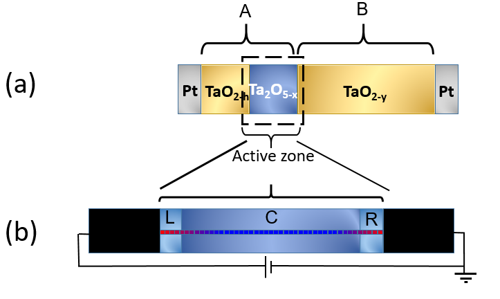
Based on combined STEM-HAADF and XPS analysis, we characterize our virgin devices as Pt/Ta2O4.70/TaO1.67/Pt, as shown in the sketch displayed on Figure 1(d).
We describe now the electrical characterization. The bottom Pt electrode was grounded and the electrical stimulus (voltage) was applied to the top Pt electrode.
The devices were initially in a low resistance state (100 ; an electroforming process with negative stimulus (i.e. -3 V pulses, with a 1 ms width) was necessary to increase the devices resistance to the range of k and activate their memristive behaviour. After forming, dynamic current-voltage (I-V) curves were obtained by applying a sequence of voltage pulses of different amplitudes (0, with a time-width of 1ms and a step of 100 mV), with the current measured during the application of the pulse. Additionally, after each voltage pulse a small reading voltage was applied to allow the current to be measured and the remnant resistance state determined, obtaining the HSL. We have found that the devices electrical response is highly dependant on both and .
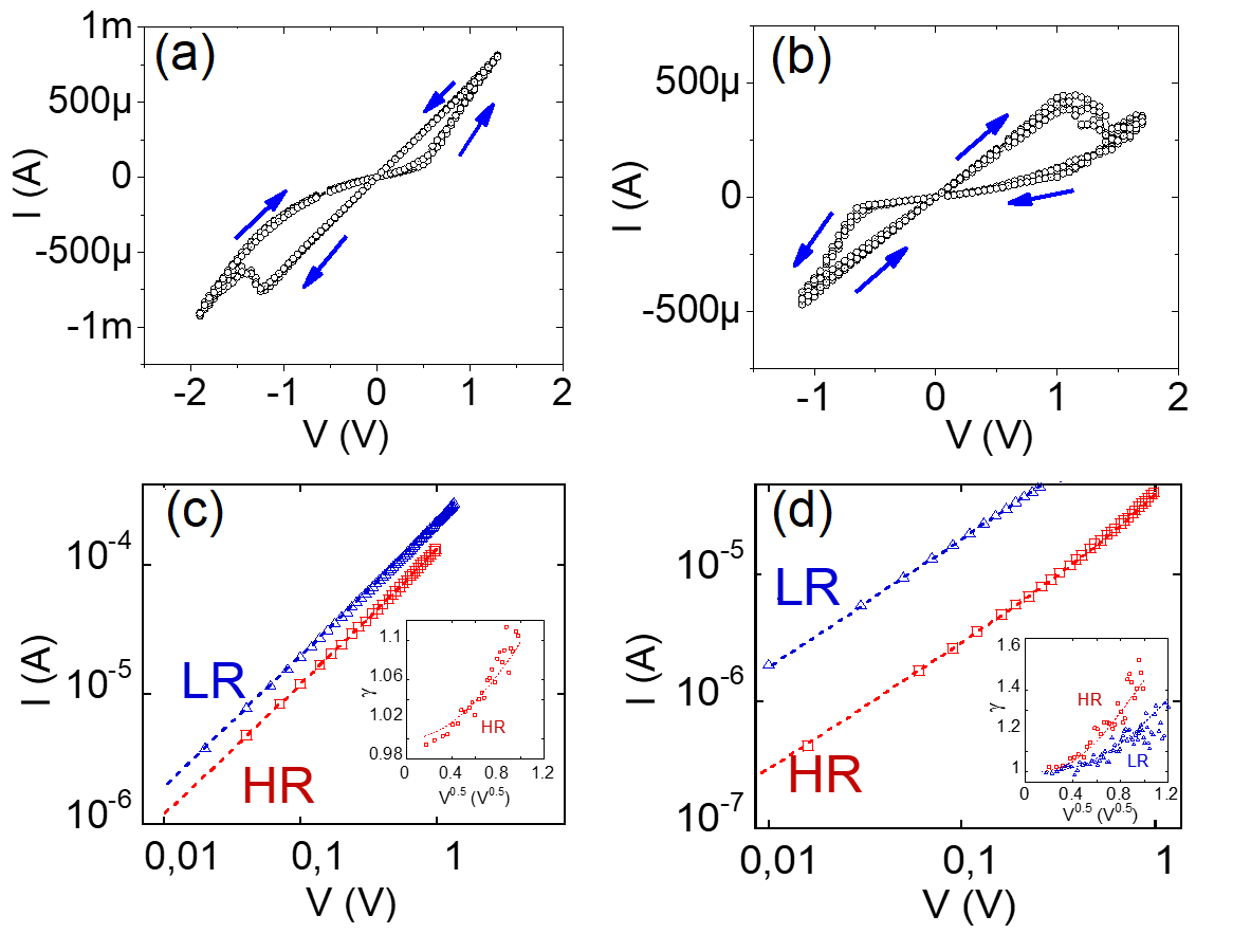
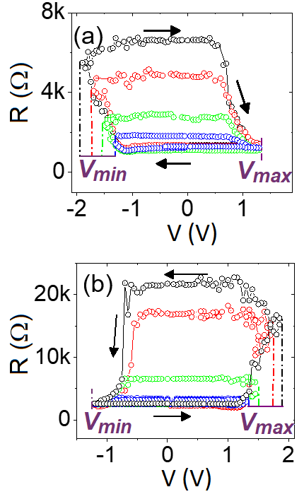
Figures 3 (a) and 4 (a) display respectively, the dynamic I-V curve and HSL obtained for a device with 28x103 m2 area, for = +1.5 V and = -2 V. It is found that the transition from HR2 to LR2 (SET process, the notation of the resistive states is chosen to be consistent with the fittings and simulations to be described below) is achieved with positive stimulus ( +1V) while the opposite transition (RESET) is obtained with negative voltage ( -1.2 V). The LR2 and HR2 states are 0.8 k and 2.5 k respectively, giving an ON-OFF ratio of 3.1. The stability and reproducibility of the curves is remarkable, as shown in Figure S2 of the Suppl. Information for 200 consecutive cycles. In addition, retention times up to 104 s were checked for both resistive states.
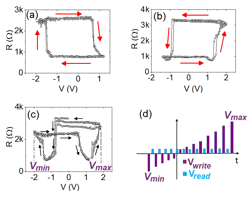
From these measurements, it is established that the HSL present a clockwise (CW) circulation. Remarkably, this circulation is inverted to a counter-clockwise (CCW) behaviour when the maximum voltage excursion are inverted to = +2 V and = -1.5 V, as shown in Figures 3 (b) and 4 (d), respectively. In this case, the transition from HR1 to LR1 (SET process) is achieved with negative stimulus ( -1V) while the opposite transition (RESET) is obtained with positive voltage ( +1.5 V). The LR1 and HR1 states in this case are 1 k and 3.3k respectively, giving an ON-OFF ratio of 3.3. Again, an excellent stability upon consecutive cycling is found (200 cycles), as shown in Fig. S2 of the Supp. Information, and retention times for up 104s were also checked. These results clearly show that the circulation of the HSL can be controlled and tuned on the same device by properly choosing the voltage excursions of applied stimuli. The inverse dependance of LR1 and LR2 states with the device area (shown in Figure S3 of the Supp. Information) indicates the existance of conducting paths comprising the complete device area.
Interestingly, if the voltage excursions are enlarged and symmetrized to =2 V, the HSL change from squared to a TWL-like shape, as shown in Figure 4 (c). The squared HSLs of Figures 4 (a) and (b) correspond to a single active interface while the TWL of Figure 4 (c) corresponds to two complementary active interfaces; that is, when one switches from low to high resistance the other one changes inversely Rozenberg et al. (2010). These results clearly indicate that our two memristive series interfaces can be selectively decoupled and activated by means of the application of proper electrical stimuli, and goes against previous claims about the “simultaneous” memristive behavior of two series interfaces Jeong et al. (2009).
We have found that for both (squared) HSL circulations multilevel states are possible. Figure 5 (a) shows, for a device with 11.3x10³ m2 area, that different non-volatile resistance levels can be achieved for CW HSLs upon increasing from 1.3 to 1.9 V, while keeping fixed at -1.9 V. In a similar way, Figure 5 (b) shows a multi-level behavior for a CCW HSL upon changing from -1.3 V to -1.9 V while keeping =1.2 V fixed. We note that this device presents higher remanent resistance states due to its lower area in relation to the previously described devices of Figures 3 and 4.
The multilevel resistance states show that our devices behave in an analogic way, which is a key feature to mimic the adaptable sinaptic weight of biological synapsis.
In order to understand the described behavior, we start with the forming process. Virgin devices are found in a low resistance state, indicating that the more oxidated A layer (with an average stochiometry Ta2O4.70, according to STEEM-HAADF experiments) presents a substantial higher conductivity that the one expected for the insulating stochiometric compound. This can be explained both by the presence of strong oxygen deficiency and to some material inhomogeneity at the nanoscale (see Figure S1 of the Supp. Information), which allow the presence of percolative low resistance Ta-rich paths bridging the nearby layers. However, as both TaO2 and TaO present at the B layer are metallic Prakash et al. (2013), the A layer still dominates the resistance of the oxide bilayer. The application of negative voltage to the top (left in Figure 6 (a)) electrode triggers an electroforming process that increases the resistance of the device by inducing the migration of OVs within the A layer, as the electrical field acting on this layer is higher that the one acting on the more reduced B layer. Oxygen ions are pushed down within the A layer (from left to right in the scheme of Figure 6 (a)), leading to the formation of a nearly stochiometric Ta2O5-x, resistive, layer and a strongly reduced, metallic, layer in contact with the Pt top (left zone in Figure 6 (a)) electrode. The presence of this reduced layer is infered from the symmetric and non-rectifying behavior observed in the post-forming I-V curves (Figures 3 (a) and (b)) which rule out the presence of Ta2O5-x in contact with the left Pt electrode, as the Pt/Ta2O5-x interface is known to present rectifying (Schottky) behavior Zhuo et al. (2013); Lee et al. (2011).
Interestingly, we have found that if the forming process is done with positive voltage, a rectifying behavior is observed in the I-V curves, indicating that in that case the formed Ta2O5-x layer is in contact with the top Pt electrode, consistently with the inversion of the forming polarity (see Figure S4 of the Supp. Information). We return now to the negative forming scenario.
Unlike the case of Ti-oxides, which display a large number of stable sub-stochiometric phases with less oxygen content than TiO2 Okamoto (2001), the commonly accepted Ta-oxide phase diagram only allows stable Ta2O5 and Ta(O) -that is metallic Ta with some diluted oxygen- phases Garg et al. (1996). TaO2 has been considered as a metastable phase Yang et al. (2010a), but recent reports claim that it might be stable with an even lower potencial energy than Ta2O5 Wei et al. (2008); Yang et al. (2010b). This suggests that the as-grown A layer, with nominal Ta2O4.70 composition, might be a metastable phase that is phase separated during forming, due to Joule heating Yang et al. (2010a), into nearly stochiometric stable Ta2O5-x and TaO2-h layers (x,h 1), as depicted in Figure 6 (b). If we assume that the forming process only involves oxygen redistribution within the A layer, it can be estimated that the thickness of Ta2O5-x and TaO2-h layers layers are about 90 % and 10 % of the initial A layer thickness.
We remark that in the post forming state the Ta2O5-x resistive layer is sandwiched between two reduced metallic TaO2-h and TaO2-y layers, giving a quasi-symmetric geometry, as shown in the zoomed sketch of Figure 6 (b), which explains the HSL with TWL-like shape obtained for symmetric stimuli (Figure 4 (c)), typical of symmetric devices.
The scenario proposed above is supported by the following analysis and fittings performed on the post forming I-V curves, considering the = dLn(I)/dLn(V) parameter representation Acha (2017). This method proved to be useful in order to reveal the presence of a mixture of conduction mechanisms Acha et al. (2016); Acevedo Román et al. (2017), as usually found in oxide-based devices Acha (2011); Cerchez et al. (2013); Blasco et al. (2015). As can be observed in the insets of Figures 3 (c) and (d), associated with both CCW and CW HSLs of devices with 6.4x10³ m2 area, the dependence of vs V1/2 indicates the existence of an ohmic conduction ( 1 at low voltages) in parallel with a mild non-linear space charge limited current (SCLC) conduction ( increases smoothly with V and remains 2).
The simplest schematic circuit representation derived from the voltage dependence of the parameter consists in two parallel SCLC-ohmic conducting channels in series. The experimental I-V curves were fitted by considering the equivalent circuit and related equations included in the Supp. Information. The performed fits give an excellent reproduction of the experimental I-V characteristics as well as the associated vs. V1/2 curves, as shown in Figures 3 (c) and (d). We notice that no good fitting was obtained if Schottky emission is assumed for the non-linear element of the equivalent circuit. This fact, together with the already discussed non-rectifying behavior observed in the I-V curves (Figures 3 (a) and (b)) rule out the presence of Ta2O5-x in contact with the left Pt electrode, giving consistency to the proposed post-forming scenario.
| HSL | STATE | R | R(0.1V) | R(1V) | R | R(0.1V) | R(1V) | Rrem |
|---|---|---|---|---|---|---|---|---|
| CCW | HR | 34.2 | 1700 | 70 | 0.8 | - | - | 34.3 |
| LR | 5.2 | 620 | 25 | 0.1 | - | - | 5.3 | |
| CW | HR | 0.1 | - | - | 8.4 | 770 | 8 | 8.4 |
| LR | 0.1 | - | - | 5.1 | 500 | 50 | 5.1 |
The memristive and non-linear behaviours are nicely reflected in the extracted values of the equivalent circuit elements, listed in Table 1. As can be observed, the electric response associated with the CCW HSL is dominated by R1 and R elements, as the R2 resistor is highly metallized, shortcircuiting the R non-linear element. The remnant resistance measured al low-voltage bias (0.1 V) is essentially the equivalent resistance R between R1 and R. When the electric response switches to the CW HSL, the situation is reversed: R1 shortcircuits the non-linear R element and the resistance of the device is dominated by the parallel combination between R2 and the non-linear R element. As can be seen in Table 1, the determined equivalent resistances at low voltage (100mV) perfectly match the measured remanent values Rrem.
The physical origin of the observed memristive behavior can be understood in terms of OVs electromigration between a (bulk) central zone, the Ta2O5-x layer, and the interfacial zones close to TaO2-h and Ta2-y layers, respectively. To achieve a behavior consistent with the migration of OVs induced by the electric field, the CCW HSL should be represented by an active SCLC-ohmic zone, represented by the parallel R1 and R circuit elements, which includes the left interface with TaO2-h plus the central Ta2O5-x zone (we recall that SCLC is a bulk conduction mechanism) where the memristive effects esentially modify this sector, while the ohmic element R2 represents the right interface with TaO2-y, characterized by a rather low resistance. On the contrary, for the CW HSL, the increase of the amplitude of the negative applied pulses switches the active element to a zone comprising the right interface with TaO2-y plus the central bulk zone, both represented by R2 and R, increasing its resistance and concomitantly decreasing the resistance of the R1 ohmic element, which now short-circuits the SCLC R element (see Supp. Information for a sketch depicting these situations).
In the next section we will carefully address by means of simulations the OV dynamics linked to this behavior.
III Numerical Simulations
Based on the previous description, we analize here the electrical response obtained with the voltage enhanced oxygen vacancies drift (VEOV) model, which allows simulating OV dynamics at the nanoscale, linked to the memristive behavior of our devices. We start by reviewing the main equations, and we refer the readers to References Rozenberg et al., 2010; Ghenzi et al., 2013, for further details.
We consider that the active memristive region is the Ta2O5-x layer, which is assumed to consist of three zones: a central (bulk) one labelled as C and two zones, left (L) and right (R), localized close to the interfaces with the metallic TaO2-h(y) layers, which present different properties due to the presence of interfacial disorder or defects. A sketch of the assumed memristive active zone is shown in Figure 6 (b). For the modelling we suppose a 1D chain of total sites. The first sites correspond to the L layer, the following sites are assigned to the central C layer and the last sites are linked to the R layer and we assume . The sites, characterized by their resisitivity, physically represent small domains of (sub)nanoscopic dimensions with an initial OVs concentration that we assume correspond to the post forming state.
An universal feature of oxides is that their resistivity is affected by the precise oxygen stoichiometry. In particular, Ta2O5 behaves as an n-type semiconductor in which oxygen vacancies reduce its resistivity. Therefore, we write the resistivity of each site as a linear decrescent (most simple) function of the local OV density , namely:
| (1) |
where is the residual resistivity for negligible OV concentration () and Ai is a factor that changes between C, L and R layers, satisfying . We consider AL, AR AC, which implies that the resistivity of the interfacial zones is less sensitive to the presence of OV due to the presence of disorder or defects. Also, the coefficients can be taken for each layer either smoothly dependent on the site position or as constants (as we do for simplicity), without affecting the qualitative behaviour of the simulated results si .
Following Equation(1), the total resistivity of the system is given by:
| (2) |
being .
Given an external voltage applied at time , the OV density at site i is updated for each simulation step according to the rate probability , for a transfer from site i to a nearest neighbor j= i . Notice that is proportional to the OV density present at site i, and to the available concentration at the neighbour site j. In order to restrict the dynamics of OVs to the active region, we take . In addition as the total density of vacancies is conserved, for each simulation step it is satisfied that , being the OV density per site for an uniform distribution (assumed as known, see Supp. Information section).
In the Arrhenius factor, , is the local potential drop at site i defined as with and the activation energy for vacancy diffusion in the absence of external stimulus. We consider values of and for the L, C and R layers respectively. All the energy scales are taken in units of the thermal energy si .
According to standard RS experiments, we chose the stimulus as a linear ramp following the cycle . At each simulation time step we compute the local voltage profile and the local voltage drops and employing the probability rates we obtain the transfers between nearest neighboring sites. Afterwards the values are updated to a new set of densities , with which we compute, at time , the local resistivities , the local voltage drops under the applied voltage , and finally from Eq.(2) the total resistivity , to start the next simulation step at . Notice that as de VEOV is a 1D model, the conversion from resistivity to resistance is a trivial scale factor. We refer to the Supp. Information si for further details on the numerical values of the parameters employed in the simulations.
As it was already described in Sec.II, the negative forming sets the device in a high resistance state, associated to which we define an initial OV density profile, , to start with the numerical implementation of the VEOV model. This initial OVs profile is chosen to guarantee the post forming high resistance state, in which the C zone contributes with the dominant resistance, while L and R layers present both a lower resistivity due to a large density of OVs, and contribute little to the total resistance (see Figure7 III) (a) for a scketch of the initial post forming state).
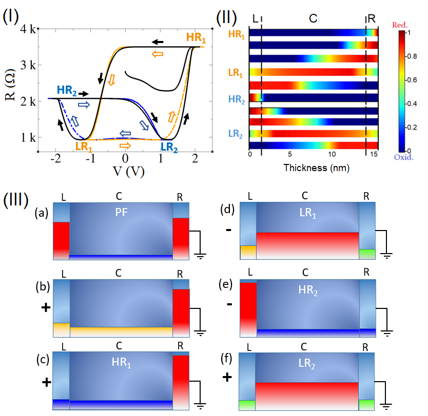
Figure 7 panel I) shows the TWL-like HSL obtained with the VEOV model simulations, for a symmetric voltage protocol following the cycle 0 Vm1=2.1 V -Vm2 =2.1 V . We start from an initial OVs distribution compatible with the post forming state, scketched in panel III) (a). This initial profile gives a resistance of 3K, in perfect agreement with the reported experimental value. The positive stimulus moves OVs from the L layer into the C layer (see panel III)(b)), initially tending to reduce the resistance. However, as the applied voltage is increased a strong electric field develops, moving OVs further away to accumulate finally in the R layer. This gives the RESET transition to the HR1 state displayed in the HSL of panel I). The associated OVs density profile along the active region is shown in the colour map of panel II) whilst the total density of OVs in the L, C and R regions respectively, is sketched in panel III) (c). The HR1 state is mantained in the range , until the polarity of the stimulus changes and consequently OVs reverse their motion. For -1.4 V a SET transition to the LR1 state takes place. The associated OVs distribution is shown in panel II) (row labeled LR1) with the color level in each of the L, C and R regions scketched in panel III)(d), proportional to the total OV density respectively. Notice that the R layer is mostly depleted from OVs which accumulate in the C layer. In spite of this accumulation, zone C still dominates the device resistance in the low resistance state LR1. Increasing further the intensity of the negative voltage, produces the electromigration of OV from the C to the L layer, almost voiding of OVs the C layer and promoting a second RESET transition to the HR2 state at a voltage 2 V (see also row labeled HR2 in panel II) and panel III) (e)). The OVs density profile for this case results slightly different from the previous one obtained for the HR1 state, giving HR2 HR1, in fully agreement with the experimental TWL-like HSL. The HR2 state is mantained until the voltage changes to possitive values and the OVs electromigrate from the L to the C layer, attaining the LR2 state at V.
The agreement between the simulated and the experimental TWL-like HSL show in Figure 4 (c) is remarkable, denoting the predictive power of the VEOV model. For completness, OV’s density profiles numerically obtained for other intermediate resistance states are also displayed in different rows of panel II).
By changing to a non-symmetrical voltage protocol we go from the TWL-like HSL to squared HSL’s, emulating the experimental response. The CW squared HSL (blue) shown in Figure 7 panel (I) was obtained for a voltage protocol =1.4 V =2.1 V , whilts the CCW HSL (orange) corresponds to a voltage protocol =2.1 V =1.4 V .
IV Discussion and conclusions
The experiments and modeling described in the present work show that it is possible to selectively activate/deactivate two series memristive interfaces in order to obtain squared CW, CCW or a TWL-like HSLs just by controlling the maximum (0) and minimum (0) applied voltage excursions. This behaviour is independent of the nature of the used electrodes: we found it in Pt/TaO2-h/Ta2O5-x/TaO2-y/Pt devices, but also in similar systems where the top Pt electrode was replaced by Au, as reported in Fig. S5 of the Suppl. Information.
A key factor that allows the obtained selective response is a forming process that changes the initial asymmetric Ta-oxide bilayer, grown at different oxygen pressures, to a quasi-symmetric TaO2-h/Ta2O5-x/TaO2-y stack, excluding the Pt(Au)/TaO2-h(y) metal-metal interfaces from contributing to the memristive behavior. The finding of CCW and CW HSLs in a single quasi-symmetric device goes against the common wisdom that, for interface-related memristors, “(a)symmetric systems give (a)symmetric electrical response”. We propose, based on our thourough analysis and modeling, that the physical origin of the obtained electrical behavior relies on OVs electromigration between bulk and interfacial zones of the Ta2O5-x layer, sandwiched between metallic TaO2-h(y). From the combination of experimental results and simulations it can be stated that for CCW HSL the OVs dynamics is constrained to C and L zones, while for CW HSL the OV exchange is limited between C and R layers. For symmetric stimuli all L, C and R are involved and the memristive response becomes symmetric (TWL-like HSL).
It can be concluded that OV transfer between one interface (i.e. R) and C zone does not start until the other interface (i.e. L) is almost completely drained of OV. This 2-steps process is the core of the observed behavior. It is worth to remark that this rich phenomenology was found for a system with a rather simple room temperature fabrication process that includes only one oxide -Ta-oxide- and one metal, suggesting that it might be possible to take advantage of these properties at low cost and with easy scability.
Regarding possible applications, the control of the symmetry of the electric response allows optimizing, for example, ON-OFF ratios for RRAM memories; however, the results presented here have potentially more implications for the development of disruptive electronics such as neuromorphic computing or novel logic devices. The observation of multilevel resistance states indicates that our devices can mimic the (analogic) adaptable synaptic weight of biological synapsis. Importantly, the multilevel states were found for both CCW and CW HSLs, indicating that the synaptic weight could be either potentiated or depressed with electrical stimulus of the same polarity. This might have implications for novel, beyond von Neummann, devices Zhang et al. (2018).
V Experimental section
Ta-oxide thin films were deposited on commercial platinized silicon by pulsed laser deposition at room temperature from a single phase Ta2O5 ceramic target. We used a 2-steps deposition process with oxygen pressures of 0.01 and 0.1mbar, resulting in 35nm and 15nm layers, respectively, as shown in the main text. The laser fluence was fixed at 1.5 J/cm2. For spectroscopic measurements, we also deposited single TaOx layers at 0.01 and 0.1mbar of O2, respectively. A Dual Beam Helios 650 was used to acquire scanning electron microscopy images and prepare FIB lamellas to observe cross-sections. High resolution scanning transmission electron microscopy was performed using a FEI Titan G2 microscope at 300 kV with probe corrector and in situ EELS spectrum acquisition with a Gatan Energy Filter Tridiem 866 ERS. The surface composition analysis obtained by X-Ray Photoelectron Spectroscopy (XPS) used a standard Al/Mg twin anode X-ray gun and a hemispherical electrostatic electron energy analyzer. The base chamber pressure was 10-9 mbar. Top Pt electrodes, 20nm thick, were deposited by sputtering and microstructured by optical lithography. Top electrode sizes ranged between 6.4x10³ and 78.5x10³ m2. Electrical characterization was performed at room temperature with a Keithley 2612 source-meter connected to a Suss probe station.
acknowledgements
We acknowledge support from INN-CNEA, UNCuyo (06/C455), ANPCyT (PICT2014-1382, PICT2016-0867, PICT2017-1836, PICT 2017-0984), CONICET (PIP 11220150100653CO) and Univ. Buenos Aires (UBACyT 20020170100284BA). M.A. also acknowledges financial support of H2020-MSCA-RISE-2016 SPICOLOST Grant No. 734187 to perform TEM studies at LMA-INA, University of Zaragoza. S.B. thanks technical support from N. Cortes.
References
- Ielmini and Waser (2016) D. Ielmini and R. Waser, Resistive Switching: From Fundamentals of Nanoionic Redox Processes to Memristive Device Applications (Wiley-VCH, 2016).
- Borghetti et al. (2010) J. Borghetti, G. S. Snider, P. J. Kuekes, J. J. Yang, D. R. Stewart, and R. S. Williams, Nature 464, 873 (2010).
- Yu (2017) S. Yu, Neuro-inspiring computing using resistive synaptic devices (Springer International Publishing, 2017).
- Prakash et al. (2013) A. Prakash, D. Jana, and S. Maikap, Nanoscale Research Letters 8, 418 (2013).
- Lee et al. (2011) M.-J. Lee, C. B. Lee, D. Lee, S. R. Lee, M. Chang, J. H. Hur, Y.-B. Kim, C.-J. Kim, D. H. Seo, S. Seo, U.-I. Chung, I.-K. Yoo, and K. Kim, Nature Materials 10, 625 (2011).
- Shi et al. (2017) K. X. Shi, H. Y. Xu, Z. Q. Wang, X. N. Zhao, W. Z. Liu, J. G. Ma, and Y. C. Liu, Applied Physics Letters 111, 223505 (2017), https://doi.org/10.1063/1.5002571 .
- Baek et al. (2016) G. H. Baek, A. R. Lee, T. Y. Kim, H. S. Im, and J. P. Hong, Applied Physics Letters 109, 143502 (2016), https://doi.org/10.1063/1.4963884 .
- Rozenberg et al. (2010) M. J. Rozenberg, M. J. Sánchez, R. Weht, C. Acha, F. Gomez-Marlasca, and P. Levy, Phys. Rev. B 81, 115101 (2010).
- Zhang et al. (2018) H. Zhang, Y. Sijung, S. Menzel, C.-F. W. D. J. H. C. S. W. R. Funck, Carsten, and S. Hoffmann-Eifert, ACS Applied Materials and Interfaces 10, 29766 (2018).
- La Torre et al. (2017) C. La Torre, A. Kindsmüller, D. J. Wouters, C. E. Graves, G. A. Gibson, J. P. Strachan, R. S. Williams, R. Waser, and S. Menzel, Nanoscale 9, 14414 (2017).
- Park et al. (2015) T. H. Park, S. J. Song, H. J. Kim, S. G. Kim, S. Chung, B. Y. Kim, K. J. Lee, K. M. Kim, B. J. Choi, and C. S. Hwang, Scientific Reports 5, 15965 (2015).
- Park et al. (2017) T. H. Park, H. J. Kim, W. Y. Park, S. G. Kim, B. J. Choi, and C. S. Hwang, Nanoscale 9, 6010 (2017).
- Yang et al. (2012) Y. Yang, P. Sheridan, and W. Lu, Applied Physics Letters 100, 203112 (2012).
- Ghenzi et al. (2013) N. Ghenzi, M. J. Sánchez, and P. Levy, Journal of Physics D: Applied Physics 46, 415101 (2013).
- Ghenzi et al. (2014) N. Ghenzi, M. J. Sánchez, D. Rubi, M. J. Rozenberg, C. Urdaniz, M. Weissman, and P. Levy, Applied Physics Letters 104, 183505 (2014).
- Chen et al. (2005) X. Chen, N. J. Wu, J. Strozier, and A. Ignatiev, Applied Physics Letters 87, 233506 (2005), https://doi.org/10.1063/1.2139843 .
- Jeong et al. (2009) D. S. Jeong, H. Schroeder, and R. Waser, Nanotechnology 20, 375201 (2009).
- (18) See Supporting Information for details. .
- Simpson et al. (2017) R. Simpson, R. G. White, J. F. Watts, and M. A. Baker, Applied Surface Science 405, 79 (2017).
- Zhuo et al. (2013) V. Y.-Q. Zhuo, Y. Jiang, M. H. Li, E. K. Chua, Z. Zhang, J. S. Pan, R. Zhao, L. P. Shi, T. C. Chong, and J. Robertson, Applied Physics Letters 102, 062106 (2013).
- Okamoto (2001) H. Okamoto, Journal of Phase Equilibria 22, 515 (2001).
- Garg et al. (1996) S. P. Garg, N. Krishnamurthy, A. Awasthi, and M. Venkatraman, Journal of Phase Equilibria 17, 63 (1996).
- Yang et al. (2010a) J. J. Yang, M.-X. Zhang, J. P. Strachan, F. Miao, M. D. Pickett, R. D. Kelley, G. Medeiros-Ribeiro, and R. S. Williams, Applied Physics Letters 97, 232102 (2010a).
- Wei et al. (2008) Z. Wei, Y. Kanzawa, K. Arita, Y. Katoh, K. Kawai, S. Muraoka, S. Mitani, S. Fujii, K. Katayama, M. Iijima, T. Mikawa, T. Ninomiya, R. Miyanaga, Y. Kawashima, K. Tsuji, A. Himeno, T. Okada, R. Azuma, K. Shimakawa, H. Sugaya, T. Takagi, R. Yasuhara, K. Horiba, H. Kumigashira, and M. Oshima, Tech. Dig. - Int. Electron Devices Meet. 293 (2008).
- Yang et al. (2010b) Y. C. Yang, C. Chen, F. Zeng, and F. Pan, Journal of Applied Physics 107, 093701 (2010b).
- Acha (2017) C. Acha, Journal of Applied Physics 121 (2017), 10.1063/1.4979723.
- Acha et al. (2016) C. Acha, A. Schulman, M. Boudard, K. Daoudi, and T. Tsuchiya, Applied Physics Letters 109 (2016), 10.1063/1.4955204.
- Acevedo Román et al. (2017) W. Acevedo Román, C. Acha, M. Sanchez, P. Levy, and D. Rubi, Applied Physics Letters 110 (2017), 10.1063/1.4975157.
- Acha (2011) C. Acha, Journal of Physics D: Applied Physics 44, 345301 (2011).
- Cerchez et al. (2013) M. Cerchez, H. Langer, M. El Achhab, T. Heinzel, D. Ostermann, H. Lüder, and J. Degenhardt, Applied Physics Letters 103, 033522 (2013).
- Blasco et al. (2015) J. Blasco, N. Ghenzi, J. Suñé, P. Levy, and E. Miranda, Microelectronics Reliability 55, 1 (2015).