Hyperbolic Phonon Polariton Electroluminescence as an Electronic Cooling Pathway
Abstract
Engineering of cooling mechanism is of primary importance for the development of nanoelectronics. Whereas radiation cooling is rather inefficient in nowadays electronic devices, the strong anisotropy of 2D materials allows for enhanced efficiency because their hyperbolic electromagnetic dispersion near phonon resonances allows them to sustain much larger () number of radiating channels. In this review, we address radiation cooling in 2D materials, specifically graphene hexagonal boron nitride (hBN) heterostructures. We present the hyperbolic dispersion of electromagnetic waves due to anisotropy, and describe how the spontaneous fluctuations of current in a 2D electronic channel can radiate thermal energy in its hyperbolic surrounding medium. We show that both the regime of (i) thermal current fluctuations and (ii) out-of-equilibrium current fluctuations can be described within the framework of transmission line theory leading to (i) superPlanckian thermal emission and (ii) electroluminescent cooling. We discuss a recent experimental investigation on graphene-on-hBN transistors using electronic noise thermometry. In a high mobility semimetal like graphene at large bias, a steady-state out-of-equilibrium situation is caused by the constant Zener tunneling of electrons opening a route for electroluminescence of hyperbolic electromagnetic modes. Experiments reveal that, compared to superPlanckian thermal emission, electroluminescent cooling is particularly prominent once the Zener tunneling regime is reached: observed cooling powers are nine orders of magnitude larger than in conventional LEDs.
I Introduction
Heat transfer is a key issue in nano-electronics. This is true for the silicon MOSFET technology where cooling limits device performance above modest power density [Pop2010nres, ] corresponding to a thermal conductance . With the rise of 2D (bi-dimensional) electronics [Ong20192DM, ], this problem becomes even more acute because of the minute heat capacity of the channel and the reduced thermal links to the environment. In this respect, the case of graphene-based devices is emblematic : the absence of a bandgap requires driving graphene transistors in the velocity saturation regime where Joule dissipation is prominent. In high-mobility devices, the very limited electron-phonon coupling (nonpolar material, low defect density) associated to a drop of the Wiedemann-Franz heat conduction mechanism (due to a vanishing differential conduction in the saturation regime), yields considerable electronic temperatures, up to several thousands of kelvins [Yang2018nnano, ; Andersen2019science, ; Ong20192DM, ]. In this peculiar situation where phonons remain relatively cold and thermal conduction is blocked, heat release through radiative processes becomes a major issue.
It is usually recognized that black-body radiation cooling is rather inefficient in electronic devices. This essentially stems from the large impedance mismatch at optical (infrared) frequencies between vacuum and the electron gas. From a microscopic point of view, this mismatch is related to the small density of electromagnetic modes within the light cone as compared to that of the electron gas at high temperature. This issue has been overcame in recent studies [Yang2018nnano, ; Tielrooij2018nnano, ], by using a so-called hyperbolic substrate. Within the Reststrahlen (RS) bands (which roughly corresponds to the optical phonon modes) hyperbolic materials sustain long-distance propagating hyperbolic phonon-polariton (HPhP) modes that can carry a large momentum [Biehs2012prl, ; Biehs2014apl, ; Caldwell2014ncomm, ; Dai2015nnano, ; Kumar2015nl, ; Giles2016nl, ; Low2017nmat, ]111for a recent review, see Reference [Caldwell2019nrevmat, ]. When the 2D channel becomes coupled to the HPhP modes (through their evanescent field), the whole density of states can be used to radiate power : this is the so-called super-Planckian regime [Biehs2014apl, ; Principi2017prl, ]. The enhancement of the radiated power as compared to the regular blackbody can reach up to 5 decades and is not limited by hot phonon effects thanks to the relatively long propagation length of HPhP modes.
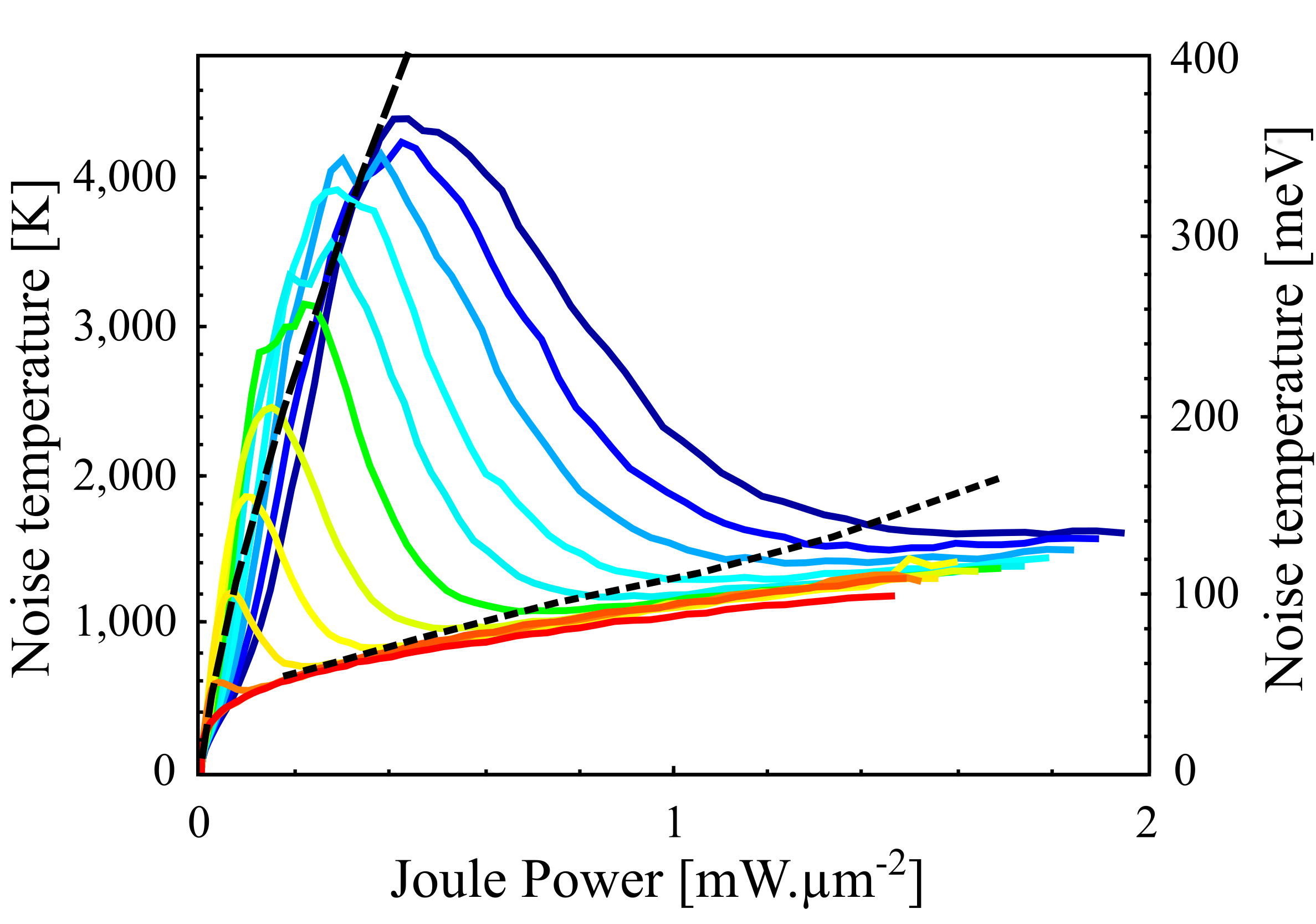
Nevertheless, the absolute cooling power remains rather limited () in the case of graphene supported on hexagonal Boron Nitride (hBN) due to the narrow acceptance spectral band of HPhPs ( in hBN) compared to the broadband spectrum of the thermal emission of hot electrons in the channel. This is very similar to the well-known poor efficiency of a bulb lamp (defined as the fraction of power emitted in the visible window) because of the broadband emission of thermal fluctuating charges in the infrared. This limitation is overcame in light-emitting diodes (LEDs) that achieve up to 90% electroluminescence conversion efficiency using a non-equilibrium distribution of electrons and holes that recombine across the band gap, thereby funneling efficiently the electrical power into the relevant visible window [Santhanam2012prl, ; Santhanam2013apl, ; Xue2015apl, ; Liebendorfer2018xxx, ]. Similarly, emission in the narrow spectral RS bands where the substrate sustains hyperbolic modes can be targeted by driving the transistor in the Zener-Klein (ZK) tunneling regime. The Zener current becomes equivalent to an electrical pumping of non-equilibrium electron-hole pairs that efficiently recombine in the hyperbolic modes of the RS bands. This striking effect is readily seen in Figure 1, where the steady-state electronic temperature of a graphene transistor is monitored (by means of noise thermometry [Betz2012prl, ; Betz2013nphys, ; Laitinen2014prb, ; Brunel2015jpcm, ; Crossno2016science, ; Yang2018nnano, ; Yang2018prl, ]) as a function of injected Joule power 222Note that noise temperature is larger than electronic temperature under high current driving, a distinction that we do not consider in this review.. The outstanding observation is a drop of the temperature for increasing injected power above a certain threshold that corresponds to the ignition of HPhP electroluminescence in the hyperbolic hBN substrate.
In this review, we show - based on both experimental results and theoretical proposals - that radiative heat transfer can be considerably enhanced to become a major cooling pathway by either engineering of optical impedance matching between the transistor channel and a hyperbolic substrate or by operating the device in a Zener-like regime where electrical pumping of electron-hole pairs funnels efficiently the injected power into the propagating hyperbolic bands of the substrate. The discussion is based on the emblematic graphene on hBN transistors but can easily be extended to other prospective active material/hyperbolic substrate couples where superPlanckian radiative cooling could yield a major improvement. The paper is organized as follows : in a first section we briefly introduce hyperbolic materials and the concepts of thermal coupling between a 2D electronic channel and a bulk hyperbolic substrate; then we investigate the case of non-equilibrium situations and the electroluminescence of HPhPs. Finally, we present experimental data for a bilayer graphene on hBN transistor where the electronic temperature is monitored through noise thermometry.
II Coupling between graphene and hyperbolic materials
Computing the thermal radiation of an electronic channel in the electromagnetic modes requires the knowledge of the electromagnetic response of the dielectric encapsulating medium which is provided by the dielectric permittivity. For an isotropic polar dielectric, the optical phonons couple to light and provide an effective dielectric response of the form
| (1) |
where is the longitudinal optical frequency, is the transverse optical frequency and is the decay rate of the optical phonon resonance. For high-quality materials, is negative in the range , as a consequence, the material is opaque in this frequency range called Reststrahlen band (RS) usually in the mid-infrared ( for hBN). A RS band is characterized by its central frequency and its width .
An anisotropic dielectric material posesses a tensorial dielectric response. For uniaxial crystals, a class including most dielectric 2D materials, in-plane (transverse ) and out-of-plane (-axis) optical phonon energies are sufficiently separated to give rise to a splitting of the Reststrahlen band into two bands. As an example, hBN possesses two well separated bands corresponding to out-of-plane OPs (type-I band, [97,103]), and in-plane OPs (type-II band, [170,200]). The energy and width of hBN RS band II makes it a much more efficient heat conduction channel, therefore, by sake of simplicity, we shall focus specifically on this band in this review (with ). 333A discussion of hyperbolicity type can be found in Reference [Caldwell2014ncomm, ]. As a consequence, for layered 2D heterostructures, the dispersion of electromagnetic extraordinary waves takes the form :
| (2) |
and, within a type II RS band, which means that the dispersion relationship is hyperbolic. Note that this occurs only for materials with low-loss optical phonon modes ; a category named hyperbolic phonon materials. The important consequence is that becomes possible within the dispersion relationship, which opens up propagative modes with high momenta that can help radiate energy.
The efficiency of hyperbolic radiative cooling depends critically on two parameters: (i) the ability of the dielectric material to efficiently couple to the current fluctuations of the metal, and (ii) the propagation depth of this radiation within the hyperbolic dielectric. These two aspects are best understood within the framework of transmission line theory 444This approach is possible thanks to the spatial Fourier decomposition of eigenmodes allowed by in-plane translational invariance of the structures considered.: Considering a 2D conductor with random 555We only consider longitudinal current fluctuations and do not consider the transverse current fluctuations because they do not couple to the extraordinary wave which is TM polarized. current density fluctuations where is the in-plane wavector, this source interacts with the TM electromagnetic modes of the substrate of optical impedance and the metal conductivity in parallel. As a consequence, the power cast by this source in its electromagnetic environment is Note that the optical impedance of the dielectric environment is defined as the ratio between the longitudinal electric field collinear to the currents in the material, and the transverse magnetic field of the extraordinary wave. It fully determines the electromagnetic response of the environment as seen from the channel’s perspective. In terms of optics, the power can be interpreted as the average flux of the Poynting vector through the channel/dielectric interface.
According to the fluctuation-dissipation theorem, for a single band, the surface density of the current fluctuations in a material of conductivity at temperature reads
| (3) |
where is the Bose occupation number. In our experiment, the hBN layer remains cold due to the presence of the gold backgate electrode. Therefore, we can neglect the back thermal flux from the hBN to the channel. The total radiative power is then 666taking into account summation over positive and negative frequencies
| (4) |
where is the impedance matching factor :
| (5) |
The matching factor (5) restricts the phase space available for radiative heat exchange. Indeed the optical impedance reads , where and is the vacuum impedance.

When the photon energy is outside the RS band, becomes imaginary when and thus . As a consequence, radiation is limited to the very narrow lightcone as represented on Figure 2 and the emitted power is very small. For monolayer graphene at in the vacuum, it represents a radiated power , where is the Stefan-Boltzmann constant, and is the average far-field emissivity of graphene [Nair2008science, ]. This corresponds to a characteristic thermal conductance . In contrast, within the RS band, remains real, and hence remains sizeable for much larger vectors, enhancing considerably the emission efficiency.
At this point we distinguish two possible causes for current fluctuations: (a) thermal fluctuations of charges (black-body radiation) and (b) non-equilibrium fluctuations of charges (electroluminescence). The next two sections will address each of them.
II.1 Thermal hyperbolic cooling
II.1.1 Matching Factor
Let us first consider thermal emission by a single band. Since RS bands are narrow , the photon population is nearly constant over a RS band and given by the occupancy at mid-band . The radiated power (4) in the RS band energy then reads
| (6) |
with
| (7) |
where is the Fermi wavevector. can be interpreted as an average impedance matching factor over the RS band. For a metal with parabolic dispersion, also corresponds to the average power radiated per electron in the conduction band. Let us note that in the degenerate case, integral over wavevector (6) is bounded in a window due to a cut-off defined by Pauli blocking.
Since most optical modes lie out of the lightcone the optical impedance is well approximated by in the infinite dielectric-thickness limit 777The finite thickness optical impedance can be found in Reference [Yang2018nnano, ]. Regarding the 2D electronic channel response, due to the significant extension of the integration window in the first Brillouin zone, the nonlocal conductivity is needed. We rely on the linear response theory for the case of non-interacting electrons in a single parabolic band:
| (8) |
where is the quantum of conductance, and are the spin and valley degeneracy, is the Fermi-Dirac occupation factor for state of wavector , is the band energy dispersion, is the chemical potential, is the effective relaxation rate of electrons, and is the periodic part of the Bloch wavefunction.
By sake of simplicity, we make the following assumptions:
-
1.
Isotropic parabolic dispersion: Except for monolayer graphene, isotropic parabolic dispersion covers most naturally occurring cases. The specific case of graphene has been dealt in detail in the literature [Principi2017prl, ].
-
2.
Unitary Bloch wave projection: Due to the small extent of the Fermi sea compared to the Brillouin zone, we can approximate
The computation of the nonlocal conductivity is given in appendix. In the degenerate case, one has , where is a simple geometric function. Consequently, the prefactor is a function of the reduced doping and of an effective light-matter coupling factor that reads
| (9) |
where is the fine-structure constant, and , where is the effective mass of the parabolic electronic band. The doping dependence of reflects the ability of the channel’s electrons to couple to the HPhP modes of the substrate.
Figure 3 represents the matching factor taking into account only the conduction band of bilayer graphene for increasing doping. The allowed transitions in the degenerate regime restrict the HPhP radiation window in the wavevector range , which is centered on .

For semimetals (like few layer graphene), the wavevector window for impedance matching is larger and extends over in the degenerate case, due to the allowed interband transitions in the thermal regime. For moderately doped graphene, , the weak electron-photon coupling is balanced by the characteristic electronic transition wavevector with respect to optical wavevector , so that . We conclude that graphene is naturally matching the naturally hyperbolic material hBN. The number of layers of graphene itself impacts obviously the radiated power due to different electronic dispersion. As a rule of thumb, we estimate a radiative cooling power of at a temperature of which translates into a thermal conductance intermediate between the experimental values in Figure 1. Finally, note that experimental observations reveal that HPhP cooling is suppressed when graphene is submitted to a quantizing magnetic field [Yang2018prl, ] because electrons localize in small cyclotron orbits forbidding wavevector matching with HPhPs.
II.1.2 Propagation depth of the HPhPs
The above evaluation of the radiated power doesn’t provide information on where heat is dissipated. To obtain an efficient heat release, the propagation depth of HPhPs must be large enough to release heat remotely in a large volume and avoid hot-phonon effects. The characteristic propagation depth of the HPhPs is given by For large in-plane k-vector compared to , the characteristic wavevector in a RS band is At center frequency , field propagation is maximal and reaches
| (10) |
In the case of bilayer graphene on hBN, the characteristic wavector of near-field radiative heat exchange is for which the propagation depth reaches 240 . Note that the presence of a nearby metallic back gate, with a low optical impedance, will reflect HPhPs and eventually lead to the reabsorption of the emitted power after one round trip. This situation occurs in thin hBN samples such as in Reference [Yang2018nnano, ]. This is avoided in the back-gated device analyzed below where the hBN thickness () exceeds , so that a full HPhP cooling can be observed.
II.2 Electroluminescence in a Hyperbolic Material
Electroluminscence is associated with interband optical conductivity occurring when electron-hole pairs are electrically pumped from the valence to the conduction band, a situation which occurs spontaneously in high mobility graphene when a large bias is applied [Yang2018nnano, ]. The electroluminescence results from the interband recombination of electron-hole pairs. Whereas classical electroluminescence is limited to vertical transitions, this emission process can also be considerably boosted when high- propagating modes are available in the dielectric. In this section we focus on the excess radiation power related to electroluminescence.
The theoretical treatment of electroluminescence is closely related to near-field thermal emission, except that out-of-equilibrium current fluctuations are given by the nonlocal van Roosbroeck-Shockley relation for interband transitions [Wurfel1982jpc, ; Rosencher2002cambridge, ; Greffet2019prx, ]:
| (11) |
where with is the photon chemical potential associated to the difference in chemical potential between the two bands of interest (denoted as and ). Note that this approximation assumes an ultra-fast electron-electron thermalization, and the existence of two pseudo Fermi distributions in the valence and conduction bands. The interband nonlocal conductivity, , is evaluated on the interband transitions between the bands of interest. The total radiated power is the sum of power radiated by all intraband and interband transitions. Focusing on the case of a pair of valence and conduction bands, the fraction of radiated power cast by electroluminescence is deduced from Eqs.(4) and (5) using as the source. Note that, in this case, the impedance matching coefficients read
| (12) |
where is the intraband conductivity.
With gaped semiconductors, electroluminescence becomes important when the difference in conduction and valence chemical potential reaches the bandgap energy . In contrast to this well-known configuration, graphene has no bandgap, however, the threshold energy is now the RS band energy For unbiased graphene, out-of-equilibrium electronic distribution can be transiently created by optical pumping and have been observed to relax on sub-ps timescales by optical pump-probe techniques [Ong20192DM, ; Mak2014apl, ; Tielrooij2018nnano, ; Malic2017andp, ]. In the next section, we show that electrical pumping of charges occurs similarly in high mobility graphene under large bias and leads to a favorable situation for HPhP electroluminescence cooling.
III Hyperbolic phonon polariton electroluminescence
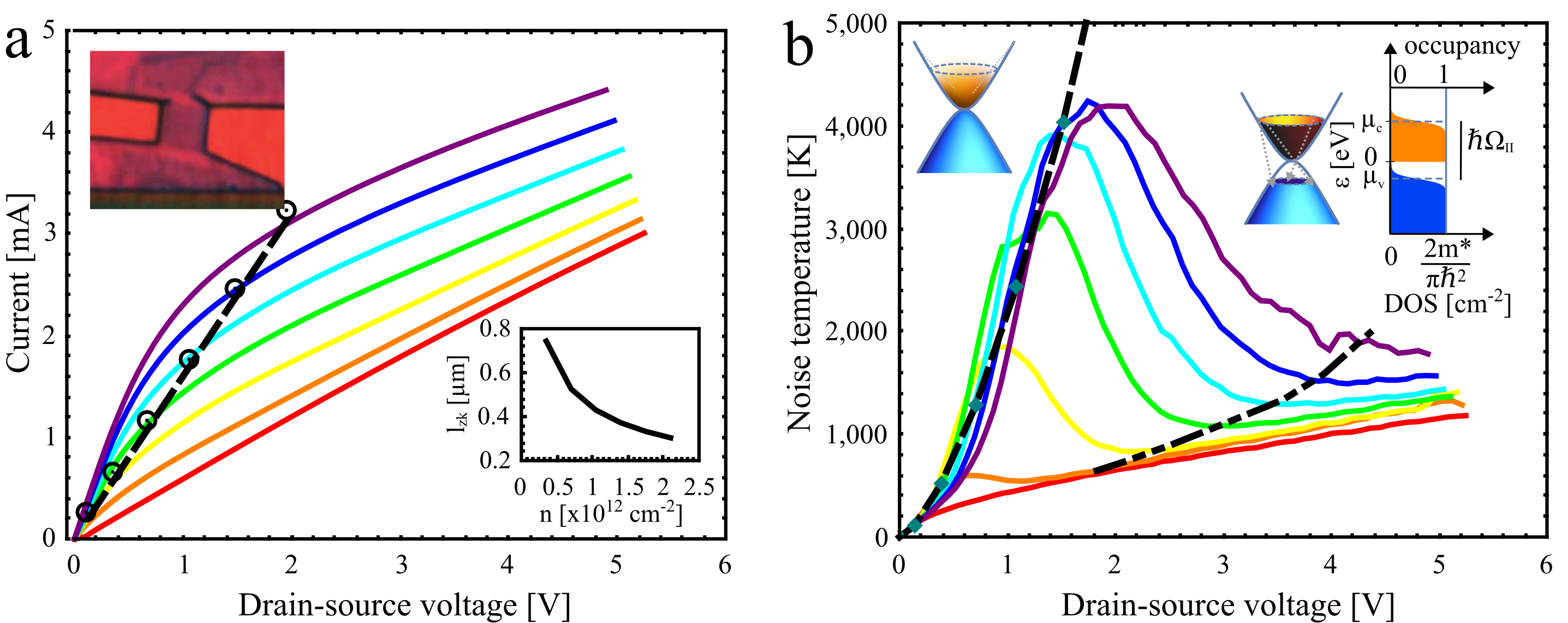
To illustrate HPhP cooling we analyze here one of the graphene ZKT transistors investigated in Reference [Yang2018nnano, ] (Figure S4 of the Supplementary Material). It is a high-mobility bilayer graphene flake, of dimensions , deposited on a -thick hBN crystal (inset of Figure 4-a). A global metallic back gate is used to tune electron density in the range . Figure 4-a depicts the transport properties of the ZKT transistor which is characterized by an initial increase of the intraband current up to a doping-dependent saturation value followed by an interband contribution with a doping-independent differential conductance . Figure 4-b shows the noise temperature characteristics.
III.1 Intraband current saturation
At moderate bias in high mobility devices, we observe a current partial saturation [Meric2008nnano, ] which is well described by the semi-empirical expression of the conductivity [Yang2018nnano, ]. Fits of the differential conductivity allows obtaining mobility and a doping-dependent saturation electric field . Mobility is large enough for intraband current saturation to be achieved at low to moderate voltage , leaving a broad experimental window for inter-band transport. The current saturation characteristic energy is deduced from the saturation electric field with . [Yang2018nnano, ] At the low to moderate doping of our experiment, we remark that current saturation is limited by the Fermi energy [Yang2018nnano, ].
III.2 Zener-Klein tunneling
We recall here the properties of the high-bias Zener-Klein regime introduced in Reference [Yang2018nnano, ]. Assuming a uniform electric field, one can express the doping-independent Zener-Klein resistance as the series addition of incoherent tunneling processes taking place over a length with an elementary conductance , where is the number of transverse electronic channels involved in electronic conduction, and is a smooth junction factor 888 was labeled in reference [Yang2018nnano, ] (bilayer graphene [Yang2018nnano, ]). This leads to an apparent Zener-Klein conductivity , because each electron-hole pair spontaneously created by Zener tunneling diffuses over a length before recombining separately with conjugated charge carriers. Experimentally, one can extract the product from the constant differential conductance . Zener-Klein tunneling being controlled by Pauli blocking, its ignition is subject to a threshold field . If mobility is large enough, the intraband current is saturated prior to the onset of Zener-Klein tunneling so that . This defines the intraband/interband transport boundary as the line , highlighted as a black dotted line in Figure 4-a. Note in passing that saturation currents do reach the intrinsic limit (symbols in the dotted line of Figure 4-a) in this sample. From the slope of the line we extract , and finally deduce (lower inset of Figure 4-a). The dependence, indicates that the electron-hole diffusion length is proportional to the average distance between charges. Remarkably enough, transport does not show any indication of thermal degradation at high bias in spite of the large Joule power , which is three orders of magnitude larger than the limit for thermal degradation in MOSFETS [Pop2010nres, ]. To get a deeper insight on the physical origin of this hyper-cooling we rely on the noise analysis below.
III.3 Hyperbolic phonon polariton cooling
As explained in the experimental section below, a Johnson-Nyquist noise temperature can be deduced from the GHz current noise and differential conductance . Its bias voltage dependence in Figure 4-b reveals very contrasted behaviors for intraband and interband transport. The former corresponds to a a superlinear bias dependence at low bias [Yang2018nnano, ] and a quasi-linear dependence at high bias. Remarkably the transition occurs at the Zener-Klein tunneling onset defined above according to Pauli blocking (black dotted line), and gives rise to a dramatic drop of the noise temperature (or a noise plateau for graphene transistors with thin hBN dielectric [Yang2018nnano, ]). The neutrality regime provides a valuable insight on the cooling mechanism, by featuring a threshold at , which is invariantly observed in graphene allotropes (single-layer, bilayer and trilayer graphene), pointing to a phonon activation mechanism with an energy matching the type-II HPhP band of hBN [Yang2018nnano, ]. This activation energy corresponds to the “optical gap” expected for HPhP electroluminescence.
If the low-bias regime can be interpretaed in the framework of superplanck HPhP black-body emission, the high-bias regime cannot (for details see Reference [Yang2018nnano, ]). In particular, superplankian emission cannot account for the drop of temperature in increasing Joule power. An out-of-equilibrium emission of HPhPs by hot electrons in the inter-band regime is needed.
III.4 Electroluminescence hyperbolic phonon polariton cooling
A parallel with LED is helpful to understand why electroluminescence is associated to a cooling of the electron gas. In LEDs, electron-hole pairs are injected from the electrodes and recombine in the active region. The energy per injected electron-hole pair is slightly larger than the effective bandgap at the junction, and consequently, radiative recombination energy is insufficient to sink the injected energy (the situation is made even worse considering the competing nonradiative recombination). As a consequence, electroluminescence is usually associated with a small heating of the device. However, it has been reported that, for high quality devices at subthreshold bias for which , the LED acts as a refrigerator as the missing energy is provided by the thermal energy of the electron gas. To date, LED refrigerators are very inefficient with a record cooling power of only [Santhanam2013apl, ]. The graphene transistor presented in this paper operates in refrigerator mode at moderate bias where , therefore, the sudden drop in temperature at the Zener-Klein tunneling threshold is a consequence of a competition between intraband heating, and interband HPhP electroluminescent cooling. The cooling power reaches , i.e., nine orders of magnitude larger than in conventional LEDs. However, since the electron gas temperature is much larger than the phonon bath one, as a whole this graphene transistor is not a refrigerator and cooling power is not bounded by a Carnot inequality, in contrast with LEDs where the device gets colder than its environment.
The injected energy per electron-hole pair is the electrical work done by the charge during diffusion and reads , where is the Joule power associated with Zener tunneling processes, and is the rate of electron-hole pair creation by Zener-Klein tunneling. We deduce the injection energy per electron-hole pair to be . This allows obtaining the characteristic electric field for which injection energy balances HPhP emission energy by electron-hole pair recombination. This electric field defines the boundary between electroluminescent cooling and heating, it is indicated in Figure 4-b (dashed line) and it matches well the voltage for which the minimal temperature is reached.
The chemical potential imbalance between the valence and conduction band can be estimated from the data in Figure 1. For doping, the maximum temperature is reached at ZK threshold for an injected Joule power , and drop to a minimal temperature for . Assuming the cooling power variation with the electronic bath state is mainly governed by the photon occupation factor (a legit assumption because of its singular behavior at the electroluminescence–superluminescence threshold ), we deduce that the chemical potential imbalance reaches the lower boundary of the hBN RS band II. Below Zener-Klein electric field threshold, the electronic temperature results from a power balance between intraband processes only. At very high electric field, with Zener-tunneling and electroluminescence recombination increasing, the conduction and valence band reach a doping state which is mainly independent of gate-doping: , where is the Fermi energy at vanishing bias. As a consequence, the power balance tends to be dominated by Joule heating originating from ZK tunneling processes, which is independent of doping, and HPhP emission by both intraband thermal emission and interband electroluminescence defined by a similar electronic distribution. Therefore, noise temperatures obtained at finite doping tend to line up on the temperature obtained at null doping at large bias as observed on Figure 1.
IV Conclusions and perspectives
The above noise thermometry measurements in the Zener-Klein regime of a hBN-supported bilayer graphene transistor, supported by the theoretical analysis, demonstrate the superior cooling power of radiative HPhP electroluminescence. As shown in Reference [Yang2018nnano, ] the mechanism is quite generic and consistently observed in single layer, bilayer and trilayer graphene. The role of hBN thickness is emphasized here with a stronger cooling effect, and a negative thermal conductance regime reported in the semi-infinite hBN substrate regime. Theoretical modeling provides useful keys to assess the difference between supported and encapsulated graphene, and constitutes a base to tackle more involved situations such as the rich moiré phases of hBN encapsulated graphene [Bistritzer2011pnas, ; Cao2018nature, ; Yankowitz2019science, ]. Hyperbolicity of the phonon modes adds to the list of hBN qualities which include dielectric strength, compatibility with high graphene mobility [Banszerus2015sciadv, ; Banszerus2016nl, ], and optical properties [Schue2016nscale, ; Schue2019prl, ].
HPhP radiative cooling is not limited to the hBN-graphene couple. It should also be observed with graphene on calcite [Salihoglu2019jqsrt, ] or mica [Low2014small, ] which have similar hyperbolic Restrahlen bands. Graphene on mica transistors have a lower mobility possibly precluding the electroluminescent regime but still constitute are valuable route for high performance flexible electronics [Hu2018as, ]. Conductive materials such as cuprates or tetradymites (e.g. Bi2Se3-xTex) also sustain hyperbolic modes [Narimanov2015nphot, ]. The case of tetradymites deserves special attention as HPhP energy lies in the near infrared to optical range [Esslinger2014acsphot, ], which is larger than the bandgap. Their finite conductivity comes from topological surface states which can be used to realize field-effect transistors in the bulk depleted regime [Inhofer2018prapp, ]. Remarkably they combine, in one and the same material, the two properties valued in graphene-hBN heterostructures: a gapless Dirac Fermion transport at the surface and hyperbolic HPhP modes in the bulk. Finally, and possibly most impactful for applications, superplanckian HPhP cooling can be envisioned in silicon on insulator (SOI) technology [Taur1997ieee, ], provided that the -thin active channel is nested in the near-field of a hyperbolic dielectric such as -sapphire or -quartz [Winta2019prb, ]. The inclusion of an HPhP cooling stage in MOSFET technology would lift the thermal bottleneck at reported in Reference [Pop2010nres, ].
V Experimental section
V.1 Sample
Sample fabrication is described in Reference [Yang2018nnano, ]. The sample analyzed here is made of an as-exfoliated bilayer graphene flake, of dimensions , deposited on a -thick hBN crystal (inset of Figure 4-a). The use of a thick hBN dielectric (i.e. thicker than the HPhP propagation depth) avoids HPhP reflections at the metallic back gate and simplifies analysis. The sample is equipped with high-transparency contacts, a global metallic backgate, and is embedded in a coplanar wave guide (CPW) for high-frequency current noise measurement. DC current and noise are measured at liquid helium temperature (4.2), in the hole doped regime –, where we obtain a low-field mobility .
V.2 Noise thermometry principles
Noise thermometry principles, described in Reference [Yang2018nnano, ] (Supplementary), are introduced here. Electrons in a metal sustain thermal fluctuations leading to the well-known Johnson-Nyquist white current noise [Nyquist1928prb, ], proportional to the sample conductance and electronic temperature . This Nyquist formula serves as a primary thermometry and is used to estimate the out-of-equilibrium electronic temperature at finite bias [Betz2012prl, ; Betz2013nphys, ; Brunel2015jpcm, ; Laitinen2014prb, ; Yang2018nnano, ; Yang2018prl, ; Andersen2019science, ], when the heated electron gas decouples from the lattice and gets thermalized thanks to efficient electron-electron relaxation (rate ). To account for self-heating in the Nyquist formula, one substitutes by a noise temperature 999This approximation is fair at low to moderate drift velocity but may turn as an overestimate at large drift due to significant corrections, and the linear conductance by the differential conductance , taken at the noise measuring frequency.
Experimentally the finite currents entail an additional -like conductance noise, with is the Hooge constant and the total number of carriers participating to transport [Hooge1981rpp, ], obscuring thermal noise of interest at low frequency. Writing thermal noise as , where is a typical thermal Fano factor, one estimates a -corner frequency, . The large drift velocities of our high-mobility graphene yields , whence the need to measure thermal noise in the microwave band –.
VI Supporting Information
VI.1 Impedance matching in the degenerate case
In this appendix, we compute a generic expression for the nonlocal conductivity of a single parabolic electronic band in the degenerate regime . We then compute the coupling factor in the case of HPhP thermal radiation within a RS band of energy and width .
| (13) |
In the degenerate case,
| (14) |
| (15) |
Focusing now on , for a single isotropic massive band , and at null temperature and Fermi energy , and we have
| (16) |
Defining , and , we have
| (17) |
The integral is easily done and yield
| (18) |
for , whereas the case is obtained by symmetry of the integral
| (19) |
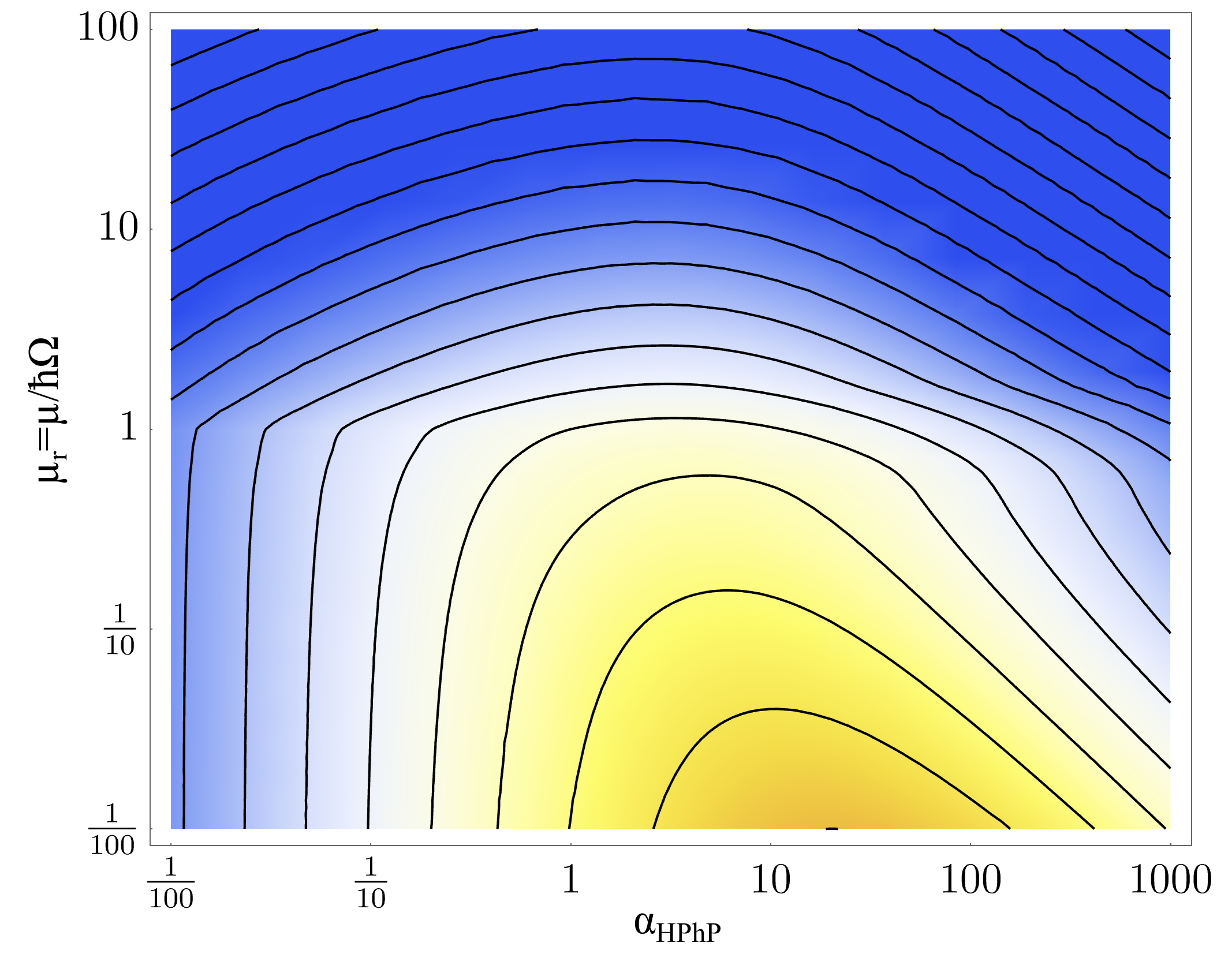
Figure 5 represents the computed factor at null temperature function of the channel/insulator properties. Corresponding illustration of the nonlocal impedance matching factor is represented on Figure 3.
The nonlocal conductivity in the degenerate case has been computed in detail for monolayer [Principi2009prb, ] and bilayer [PrincipiThesis, ] graphene and allows computing the radiated power using the above formalism (see [Principi2017prl, ] for the case of monolayer graphene).
VII Acknowledgments
The research leading to these results have received partial funding from the European Union “Horizon 2020” research and innovation program under grant agreement No. 785219 “Graphene Core”, and from the ANR-14-CE08-018-05 “GoBN”.
References
- (1) E. Pop, Nano Res. 2010, 3, 147.
- (2) Z-Y. Ong, M-H. Bae, 2D Mater. 2019,6, 032005.
- (3) W. Yang, S. Berthou, X. Lu, Q. Wilmart, A. Denis, M. Rosticher, T. Taniguchi, K. Watanabe, G. Fève, J.M. Berroir, G. Zhang, C. Voisin, E. Baudin, B. Plaçais, Nat. Nanotechnol. 2018, 13, 47.
- (4) T. I. Andersen, B. L. Dwyer, J. D. Sanchez-Yamagishi, J. F. Rodriguez-Nieva, K. Agarwal, K. Watanabe, T. Taniguchi, E. A. Demler, P. Kim, H. Park, M.D. Lukin, Science 2019, 364, 154.
- (5) K.J. Tielrooij, N.C.H. Hesp, A. Principi, M.B. Lundeberg, E.A.A. Pogna, L. Banszerus, Z. Mics, M. Massicotte, P. Schmidt, D. Davydovskaya, D.G. Purdie, I. Goykhman, G. Soavi, A. Lombardo, K. Watanabe, T. Taniguchi, M. Bonn, D. Turchinovich, C. Stampfer, A. C. Ferrari, G. Cerullo, M. Polini, F.H.L. Koppens, Nat. Nanotechnol. 2018, 13, 41.
- (6) S-A. Biehs, M.Tschikin, P. Ben-Abdallah, Phys. Rev. Lett. 2012, 109, 104301.
- (7) S-A. Biehs, M.Tschikin, R. Messina, P. Ben-Abdallah, Appl. Phys. Lett.2014, 105,161902.
- (8) J.D. Caldwell, A.V. Kretinin, Y. Chen, V. Giannini, M.M. Fogler, Y. Francescato, C.T. Ellis, J.G. Tischler, C.R. Woods, A.J. Giles, M. Hong, K. Watanabe, T. Taniguchi, S.A. Maier, K.S. Novoselov, Nat. Commun. 2014, 5, 5221.
- (9) S. Dai, Q. Ma, M. K. Liu, T. Andersen, Z. Fei, M. D. Goldflam, M. Wagner, K. Watanabe, T. Taniguchi, M. Thiemens, F. Keilmann, G. C. A. M. Janssen, S-E. Zhu, P. Jarillo-Herrero, M. M. Fogler, D. N. Basov, Nat. Nanotechnol. 2015, 10, 682.
- (10) A. Kumar, T. Low, K.H. Fung, P. Avouris, N.X. Fang, Nano Lett. 2015, 15, 3172.
- (11) A. J. Giles, S. Dai, O. J. Glembocki, A. V. Kretinin, Z. Sun, T. Chase, T. Ellis, J. G. Tischler, T. Taniguchi, K. Watanabe, M. M. Fogler, K. S. Novoselov, D. N. Basov, J. D. Caldwell, Nano Lett. 2016, 16, 3858.
- (12) T. Low, A. Chaves, J. D. Caldwell, A. Kumar, N. X. Fang, P. Avouris, T. F. Heinz, F. Guinea, L. Martin-Moreno, F. H.L. Koppens, Nat. Mater. 2017, 16, 182.
- (13) J.D. Caldwell, I. Aharonovich, G. Cassabois, J.H. Edgar, B. Gil, D.N. Basov, Nat. Rev. Mater. 2019, DOI:10.1038/s41578-019-0124-1
- (14) A. Principi, M.B. Lundeberg, N.C.H. Hesp, K-J. Tielrooij, F.H.L. Koppens, M. Polini, Phys. Rev. Lett. 2017, 118, 126804.
- (15) P. Santhanam, D.J. Gray Jr, R.J. Ram, Phys. Rev. Lett. 2012, 108, 097403.
- (16) P. Santhanam, D. Huang, R.J. Ram, M.A. Remennyi, B.A. Matveev, Appl. Phys. Lett. 2013, 103, 183513.
- (17) J. Xue, Y. Zhao, S.H. Oh, W.F. Herrington, J.S. Speck, S.P. DenBaars, S. Nakamura, R.J. Ram, Appl. Phys. Lett. 2015, 107, 121109.
- (18) A. Liebendorfer, AIP Scilight 2018, DOI:10.1063/1.5037983
- (19) A. C. Betz, F. Vialla, D. Brunel, C. Voisin, M. Picher, A. Cavanna, A. Madouri, G. Fève, J-M. Berroir, B. Plaçais, E. Pallecchi, Phys. Rev. Lett. 2012, 109, 056805.
- (20) A.C. Betz, S. H. Jhang, E. Pallecchi, R. Feirrera, G. Fève, J-M. Berroir, B. Plaçais, Nat. Phys. 2013 9, 109.
- (21) A. Laitinen, M. Kumar, M. Oksanen, B. Plaçais, P. Virtanen, P. Hakonen, Phys. Rev. B 2015, 91, 121414 (R).
- (22) D. Brunel, S. Berthou, R. Parret, F. Vialla, P. Morfin, Q. Wilmart, G. Fève, J-M. Berroir, P. Roussignol, C. Voisin, J. Phys.: Condens. Matter 2015 27, 164208.
- (23) J. Crossno, J.K. Shi, K. Wang, X. Liu, A. Harzheim, A. Lucas, S. Sachdev, P. Kim, T. Taniguchi, K. Watanabe, T.A. Ohki, K.C. Fong, Science 2016, 351, 6277.
- (24) W. Yang, H. Graef, X. Lu, G. Zhang, T. Taniguchi, K. Watanabe, A. Bachtold, E.H.T. Teo, E. Baudin, E. Bocquillon, G. Fève, J-M. Berroir, D. Carpentier, M. O. Goerbig, B. Plaçais, Phys. Rev. Lett. 2018, 121, 136804.
- (25) R.R. Nair, P. Blake, A.N. Grigorenko, K.S. Novoselov, T.J. Booth, T. Stauber, N.M.R. Peres, A.K. Geim, Science 2008 16, 1308.
- (26) P. Wurfel, J. Phys. C: Solid State Phys. 1982, 15, 3967.
- (27) E. Rosencher, B. Vinter, Optoelectronics, Cambridge University Press, 2002.
- (28) J.J. Greffet, P. Bouchon, G. Brucoli, Phys. Rev. X 2018, 8, 021008.
- (29) K.F. Mak, C.H. Lui, T. Heinz, Appl. Phys. Lett. 2014, 97, 221904.
- (30) E. Malic, T. Winzer, F. Wendler, S. Brem, R. Jago, A. Knorr, M. Mittendorff, J. C. König-Otto, T. Plötzing, D. Neumaier, H. Schneider, M. Helm, S. Winnerl, Ann. Phys. (Berlin, Ger.) 2017, 529, 1700038.
- (31) I. Meric, M.Y. Han, A.F. Young, B. Ozyilmaz, P. Kim, K.L Shepard, Nat. Nanotechnol. 2008, 3, 654.
- (32) R. Bistritzer, A.H. MacDonald, PNAS 2011, 108, 12233.
- (33) Y. Cao, V. Fatemi, S. Fang, K. Watanabe, T. Taniguchi, E. Kaxiras, P. Jarillo-Herrero, Nature 2018, 556, 43.
- (34) M. Yankowitz, S. Chen, H. Polshyn, Y. Zhang, K. Watanabe, T. Taniguchi, D. Graf, A.F. Young, C.R. Dean, Science 2019, 363, 1059.
- (35) L. Banszerus, M. Schmitz, S. Engels, J. Dauber, M. Oellers, F. Haupt, K. Watanabe, T. Taniguchi, B. Beschoten, C. Stampfer, Sci. Adv. 2015, 1, 1500222.
- (36) L. Banszerus, M. Schmitz, S. Engels, M. Goldsche, K. Watanabe, T. Taniguchi, B. Beschoten, C. Stampfer, Nano Lett. 2016, 16, 1387.
- (37) L. Schué, B. Berini, A.C. Betz, B. Plaçais, F. Ducastelle, J. Barjon, A. Loiseau, Nanoscale 2016, 8, 6986.
- (38) L. Schué, L. Sponza, A. Plaud, H. Bensalah, K. Watanabe, T. Taniguchi, F. Ducastelle, A. Loiseau, J. Barjon, Phys. Rev. Lett. 2019, 122, 067401.
- (39) H. Salihoglu, X. Xu, J. Quant. Spectrosc. Radiat. Transfer 2019, 222, 115.
- (40) C.G. Low, Q. Zhang, Y. Hao, R. S. Ruoff, Small 2014, 10, 4213.
- (41) H. Hu, X. Guo, D. Hu, Z. Sun, X. Yang, Q. Dai, Adv. Sci. 2018, 5, 1800175.
- (42) E.E. Narimanov, A.V. Kildishev, Nat. Photonics 2015, 9, 214.
- (43) M. Esslinger, R. Vogelgesang, N. Talebi, W. Khunsin, P. Gehring, S. de Zuani, B. Gompf, K. Kern, ACS Photonics 2014, 1, 1285.
- (44) A. Inhofer, J. Duffy, M. Boukhicha, E. Bocquillon, J. Palomo, K. Watanabe, T. Taniguchi, I. Estève, J-M. Berroir, G. Fève, B. Plaçais, B.A. Assaf, Phys. Rev. Appl. 2018, 9, 024022.
- (45) Y. Taur, D.A. Buchanan, W. Chen, D.J. Frank, K.E. Ismail, S-H. Lo, G.A. Sai-Halasz, R.G. Viswanathan, H-J.C. Wann, S.J. Wind, H-S. Wong, Proc. IEEE 1997, 85, 486.
- (46) C.J. Winta, M. Wolf, A. Paarmann, Phys. Rev. B 2019, 99, 144308.
- (47) H. Nyquist, Phys. Rev. B 1928, 32, 110.
- (48) F. N. Hooge, T. G. M. Kleinpenning, L. K. J. Vandamme, Rep. Prog. Phys. 1981, 44, 479.
- (49) A. Principi, M. Polini, G. Vignale, Phys. Rev. B 2009, 80, 075418.
- (50) Alessandro Principi, PhD thesis, Scuola Normale Superiore (Pisa, Italy) 2012.