Atomically-Smooth Single-Crystalline VO2 thin films with Bulk-like Metal-Insulator Transitions
Abstract
Atomically-abrupt interfaces in transition metal oxide (TMO) heterostructures could host a variety of exotic condensed matter phases that may not be found in the bulk materials at equilibrium. A critical step in the development of such atomically-sharp interfaces is the deposition of atomically-smooth TMO thin films. Optimized deposition conditions exist for the growth of perovskite oxides. However, the deposition of rutile oxides, such as VO2, with atomic-layer precision has been challenging. In this work, we used pulsed laser deposition (PLD) to grow atomically-smooth VO2 thin films on rutile TiO2 (101) substrates. We show that optimal substrate preparation procedure followed by the deposition of VO2 films at a temperature conducive for step-flow growth mode is essential for achieving atomically-smooth VO2 films. The films deposited at optimal substrate temperatures show a step and terrace structure of the underlying TiO2 substrate. At lower deposition temperatures, there is a transition to a mixed growth mode comprising of island growth and layer-by-layer growth modes. VO2 films deposited at optimal substrate temperatures undergo a metal to insulator transition at a transition temperature of 325 K with 103 times increase in resistance, akin to MIT in bulk VO2.
Growth of high quality single-crystalline thin films with atomically smooth surfaces is an essential prerequisite for the realization of heterostructures with atomically-abrupt interfaces. Such high quality interfaces could host exotic condensed matter phases that may otherwise not be realized in the bulk.Kawasaki et al. (1994); Ohtomo and Hwang (2004); Reyren et al. (2007); Brinkman et al. (2007) There is a large body of work that concerns the deposition and growth of perovskite oxide heterostructures with atomically sharp interfaces.Mannhart and Schlom (2010); Thiel et al. (2006); Salluzzo et al. (2009); Chakhalian et al. (2007) By contrast, research work on the growth of binary oxide heterostructures such as those comprising VO2 and related rutile oxides, is limited.Shibuya, Kawasaki, and Tokura (2010) This is rather surprising because the electronic properties of VO2, a prototypical correlated electron material with a metal-insulator transition, have been extensively studied both in bulk and in thin film form.Eyert (2011); Pardo and Pickett (2009); Qazilbash et al. (2007); Haverkort et al. (2005); Berglund and Guggenheim (1969); Berglund and Jayaraman (1969) VO2 undergoes a temperature-driven metal-insulator transition (MIT) from a high-temperature metallic phase to a low-temperature insulating phase at a characteristic phase transition temperature, TMIT, of 340 K.Goodenough (1971); Morin (1959) This electronic transition is concomitant with a symmetry lowering structural transition from a high temperature rutile (P42/mnm) crystal structure to a low temperature monoclinic (P21/c) crystal structure. The manipulation of MIT in VO2 via external perturbations such as strain, pressure, temperature and/or electric-field were previously attempted by several research groups in order to study the origin of MIT in this material.Berglund and Jayaraman (1969); Laverock et al. (2012); Lazarovits et al. (2010); Muraoka, Ueda, and Hiroi (2002); Nakano et al. (2012); Okazaki et al. (2004) In addition, the modification of the electronic structure of VO2 in heterostructures is attractive for the creation of novel low power oxide electronic devices such as the Mott field effect transistor (Mott-FET).Newns et al. (1998); Yajima, Nishimura, and Toriumi (2015)
In this work, we show that single-crystalline thin films of VO2 with near-ideal atomically smooth surfaces can be deposited on optimally prepared single-crystalline rutile TiO2 substrates. We further show that the films retain bulk-like sharp transitions with 103 times changes in resistance across the transition. To the best of our knowledge, the realization of near-ideal surfaces and sharp metal-insulator transitions in the same set of films has not been achieved previously. For example, the growth of VO2 on single-crystalline TiO2 (001) substrates was shown to have sharp metal-insulator transitions.Muraoka and Hiroi (2002); Aetukuri et al. (2013); Jeong et al. (2013) Unfortunately, the metal-insulator transition is suppressed to 300 K or lower making these films not suitable for devices operating at room temperature. In addition, due to the high surface energy of the rutile (001) plane, annealing TiO2 (001) substrates at temperatures that favor atomic step and terrace formation via surface recrystallization results in the undesired surface reconstruction and consequent surface roughening.Ramamoorthy, Vanderbilt, and King-Smith (1994); Diebold (2003); Aetukuri
On the other hand, TiO2 (110) surfaces have a low surface energy and are therefore amenable for annealing techniques to realize an atomic step and terrace structure.Ramamoorthy, Vanderbilt, and King-Smith (1994); Diebold (2003) However, the large and anisotropic in-plane strain imparted to the VO2 films when epitaxially deposited on TiO2 (110) substrates, usually leads to a broad metal-insulator transition.Muraoka and Hiroi (2002) Sharp metal-insulator transitions might lead to devices with high ON/OFF ratios and are therefore preferred for device applications. By contrast, when VO2 films are grown on TiO2 (101) surfaces, there is a smaller lattice mismatch when compared to the VO2 films grown on TiO2 (110) substrates. This could result in VO2 films with a sharp MIT at a transition temperature that is closer to TMIT in bulk VO2.Li and Dho (2014) Indeed, in agreement with this hypothesis, VO2 films grown on TiO2 (101) substrates have been shown to exhibit sharp transitions at TMIT of 320 K or greater.Jeong et al. (2015) In addition, TiO2 (101) surfaces have a surface energy that is intermediate between that of TiO2 (110) and TiO2 (001).Ramamoorthy, Vanderbilt, and King-Smith (1994) Therefore, it may be possible to achieve an atomic step and terrace structure, by annealing at an appropriate temperature favorable for surface recrystallization, while avoiding the undesired 3D surface reconstruction such as that observed on TiO2 (001) surfaces.Aetukuri In the following sections, we outline a reproducible procedure for realizing a step and terrace structure on TiO2 (101) substrates and show that PLD can be used to grow epitaxial VO2 (101) films that retain the step and terrace structure of the underlying substrate while also showing sharp MIT at a TMIT of 325 K.
Single-crystalline rutile TiO2 (101) substrates (Shinkosa, Japan) were treated using the following procedure. First, to remove any organic layers on the surface, as-received substrates were ultrasonically cleaned in an acetone bath (ACS Reagent grade with 99.5% purity from Merck) for 15 minutes followed by ultrasonic cleaning in an isopropyl alcohol (IPA) bath (ACS Reagent grade with 99.5% purity from Merck) for 5 minutes. Substrates were then rinsed in deionized water (resistivity 17.5 M-cm) and blow dried with nitrogen. Next, to remove trace metal contaminants from the surface, the substrates were placed in a still solution of 5 vol. % hydrochloric acid (HCl) for 5 minutes followed by rinsing with DI water and nitrogen blow drying. The substrates were then transferred to a still 50% hydrofluoric acid (HF) bath.
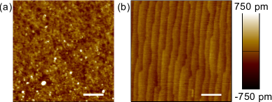
The substrates were taken out after 1 minute and immediately rinsed with DI water and blow dried with nitrogen. This chemical cleaning procedure is similar to the one previously reported by Martens et al.,Martens et al. (2014) for cleaning TiO2 (001) surfaces.
After the chemical cleaning steps (Figure 1a), the substrates were annealed at temperatures between 950 °C and 1000 °C for 4 hours under an oxygen flow rate of 10 sccm. The rate of warm up and cool down were both set to 3 °C/min. Based on our experiments, it seems that a temperature of 950 °C is necessary for recrystallization leading to the formation of a step and terrace structure (Figure 1b) with each step height being equivalent to the inter planner spacing of (101) planes. The step and terrace structure is the result of a small but non-zero miscut angle between the substrate surface and the surface of the TiO2 (101) crystallographic plane. Such surfaces are commonly referred to as vicinal surfaces. All substrates used for the growth of VO2 films in this work were annealed at temperatures between 950 °C and 1000 °C, as step-bunching was observed at temperatures higher than 1000 °C.

On vicinal surfaces, such as the surfaces of TiO2 substrates used in this work, with a near ideal step and terrace structure, heteroepitaxial growth could proceed by one or more of the three broadly classified growth modes: a) three dimensional (3D) island-growth mode (also called Volmer-Weber growth mode); b) a mixture of 2-dimensional (2D) layer-by-layer growth and 3D island growth modes (Stranski-Krastanov growth mode) and c) 2D growth mode: either layer-by-layer growth or step-flow growth modes.Gilmer and Grabow (1987); Hong et al. (2005) The preferred growth mode(s) is highly sensitive to the surface diffusivity of the constituent species (individual growth units) on the substrate surface. For example, substrate temperature is a simple yet effective parameter to tune the surface diffusivity of the growth units and therefore the growth mode.Hong et al. (2005); Koster et al. (1999) A near-ideal atomic step and terrace structure is realized when layer-by-layer and/or step-flow growth modes are the dominant growth modes. Therefore, in this work, we varied the substrate temperature while the other growth conditions were not changed as discussed below.
We employed PLD for the growth of VO2 thin films on optimally annealed rutile TiO2 (101) substrates (5 mm 5 mm 0.5 mm). All depositions were performed in a chamber with a base pressure of <5 10-9 Torr. A V2O5 pellet, prepared by compacting V2O5 powder (99.6% trace metals basis from Merck) followed by sintering at 670 °C in air for 10 hours, was used as the target. Laser energy density on the target during ablation of 1.5 J/cm2, laser repetition rate of 2 Hz, substrate to target distance of 55 mm and a background deposition oxygen pressure of 10 mTorr were used for all depositions reported in this work. Under these conditions, the growth rate was calculated (based on thickness measurements by a profilometer) to be 0.09 Å/s. As discussed later, this growth rate is also validated by in-situ high pressure reflection high energy electron diffraction (hp-RHEED) which was used to monitor growth and surface structure during deposition.
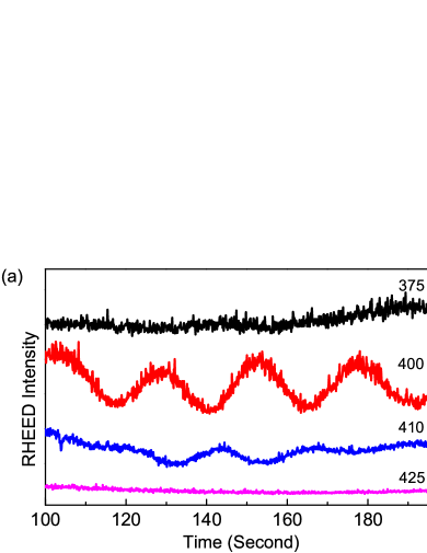
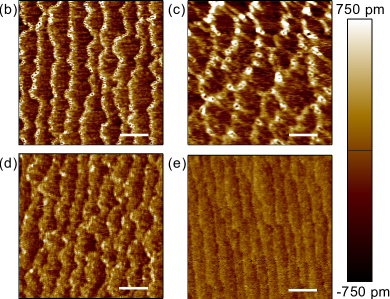
The results of temperature-dependent growth dynamics for 4 nm VO2 thin films grown on optimally annealed TiO2 (101) substrates are summarized in Figure 2. At the lowest temperature of 375 °C, we did not observe any RHEED intensity oscillations (Figure 2a); corresponding atomic force microscopy image, Figure 2b, shows an atomic step and terrace structure similar to the surface structure of the starting substrate. Notably, upon closer inspection, we observed islands at step edges suggesting that the growth mode at this temperature is a mixture of 3D island growth (at step edges) and layer-by-layer growth on the steps. At a higher substrate temperature of 400 °C, as shown in Figure 2a, we observed RHEED intensity oscillations. The average growth rate of 0.09 Å/s estimated from RHEED intensity oscillations is consistent with the growth rates estimated from profilometer measurements. However, RHEED intensity oscillations are not sufficient evidence for a truly 2-dimensional (2D) layer-by-layer growth. In fact, AFM measurements on the VO2 thin film surfaces grown at 400 °C (Figure 2c), show 3D islands at the step edges similar to the observation on the VO2 thin films deposited at a substrate temperature of 375 °C. Clearly, the linear density of islands, defined as the number of islands per unit length along the step edge and plotted in Figure 2f, decreased at the higher deposition temperature of 400 °C. We take this as indirect evidence for increased surface diffusivity of the growth units at the higher temperature. At an even higher substrate temperature of 410 °C, there is a further decrease in the linear density of islands as evidenced from AFM image shown in Figure 2d. Furthermore, the amplitude of the RHEED intensity oscillations also decreases.
Finally, as shown in Figure 2e, at the highest substrate temperature of 425 °C used in this study, we did not observe any RHEED intensity oscillations. Furthermore, the surface of the thin films showed the atomic step and terrace structure of the underlying substrate without any discernible islands at the step edges. The absence of RHEED intensity oscillations together with the observation of an atomic step and terrace structure is indicative of 2D step flow growth mode. Clearly, these changes in topography and the amplitude of RHEED intensity oscillations are consistent with the growth mode changing from a growth mode comprising of a mixture of 3D island growth and 2D layer-by-layer growth at the substrate temperature of 375 °C to a 2D step-flow growth mode at the substrate temperature of 425 °C. To the best of our knowledge, such a difference in the growth kinetics at a step edge and on the atomic steps has not been reported before. An interesting future research direction could be to explore if this difference can be exploited for directed 3D growth of, for example, VO2 nanorods on TiO2 substrates. Such directional 3D structures might find applications in tunable metamaterials based on metal-insulator transitions.Liu et al. (2012); Dicken et al. (2009); Kabashin et al. (2009)
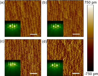
Next, we show that this step and terrace structure can be retained for VO2 film thicknesses of up to 16 nm, when thin films are deposited at the optimal substrate temperature of 425 °C. AFM images shown in Figures 3a-d for film thickness of 4 nm to 16 nm are indicative of the underlying step and terrace structure of the TiO2 substrate being retained. Furthermore, RHEED streaks that are evident in the RHEED diffraction patterns, shown in the insets of the corresponding AFM images, are suggestive of an atomically smooth 2D surface.Ichimiya and Cohen (2004) This is also evidence for the single-crystalline nature of the thin films. At much higher thicknesses, for example at a film thickness of 32 nm, we have observed cracking of the VO2 films: possibly due to interfacial strain.Kawatani, Kanki, and Tanaka (2014) Therefore, the rest of our studies are limited to films with thicknesses of 16 nm.
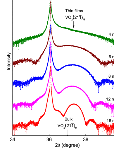
High resolution -2 X-ray diffraction (XRD) measurements (Rigaku SmartLab X-ray diffractometer) performed on VO2 thin films with thicknesses of 4 nm, 6 nm, 8 nm, 12 nm and 16 nm are evidence for the excellent crystallinity of the VO2 films (Figure 3e).
The increase in peak intensity and the decrease of full width at half maximum of the VO2 (21)M peak is in agreement with the increase in the thickness of VO2 films. Additionally, the presence of Keissig fringes in the diffractogram is indicative of a sharp interface between the VO2 film and the TiO2 substrate.
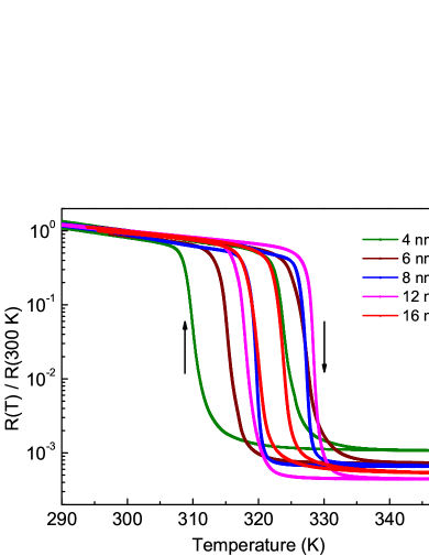
A summary of the resistance versus temperature measurements (four probe geometry using Keithley 2400 source measure units) performed while continuously heating or cooling the sample at a rate of 1 K/min is shown in Figure 4. All VO2 films show sharp metal-insulator transitions at an average TMIT of >320 K with 103 times change in resistance. Resistance normalized to the resistance at 300 K is plotted to compare the magnitude of the change in resistance of all the films; evidently, this is nearly identical for all thicknesses of VO2 films studied in this work. In addition, we did not observe any systematic changes in the transition temperature as a function of the thickness of VO2 films. There seems to be a uniform reduction in the TMIT for all films, possibly due to the VO2 film being epitaxially strained by the TiO2 substrate. This is also consistent with the X-ray measurements which show that all films in the thickness range of 4 nm to 16 nm are epitaxially strained to the substrate. An out-of-plane compressive strain of 0.9% was inferred from XRD measurements (see Figure 3e and supplementary information).
In summary, our work outlines a procedure to realize an atomic step and terrace structure on vicinal surfaces of rutile TiO2 (101) substrates. We also demonstrate that a near-ideal atomic step and terrace structure can be realized by depositing VO2 films at temperatures conducive for step flow growth. We have also observed a previously not reported mixed growth mode that comprises of a 3D growth mode at step edges and a 2D layer-by-layer growth mode on the atomic steps. Importantly, our results imply that VO2 (101) thin films as thin as 4 nm can have bulk-like transitions at a TMIT well above room temperature with R/R of 103 and are therefore suitable for device applications. Furthermore, under optimal conditions, we showed that the near ideal atomic step and terrace structure can be stabilized in VO2 films with thicknesses upto 16 nm. The growth of such atomically smooth VO2 thin films with bulk-like transitions and heterostructures comprising other related oxides such as CrO2Cai et al. (2015) could open up the possibility of developing binary oxide heterostructures. Such heterostructures could enable interfacial manipulation of metal-insulator transitions and/or play host to exotic condensed matter phases not realizable in the bulk.
The authors acknowledge CeNSE, IISc for access to HR-XRD, wire bonding and clean-room facilities. N.B.A acknowledges the new faculty start-up grant no. 12-0205-0618-77 provided by the Indian Institute of Science. N.B.A is thankful to Prof. D D Sarma and Prof. Anil Kumar for access to the PLD system. S.R.M and D.M want to thank Jibin J. Samuel for useful discussions. We thank Prof. Satish Patil for providing access to facilities supported by the Swarnajayanti fellowship under grant No. DST/SJF/CSA-01/2013-14.
References
- Kawasaki et al. (1994) M. Kawasaki, K. Takahashi, T. Maeda, R. Tsuchiya, M. Shinohara, O. Ishiyama, T. Yonezawa, M. Yoshimoto, and H. Koinuma, Science 266, 1540 (1994).
- Ohtomo and Hwang (2004) A. Ohtomo and H. Hwang, Nature 427, 423 (2004).
- Reyren et al. (2007) N. Reyren, S. Thiel, A. Caviglia, L. F. Kourkoutis, G. Hammerl, C. Richter, C. Schneider, T. Kopp, A.-S. Rüetschi, D. Jaccard, et al., Science 317, 1196 (2007).
- Brinkman et al. (2007) A. Brinkman, M. Huijben, M. Van Zalk, J. Huijben, U. Zeitler, J. Maan, W. G. van der Wiel, G. Rijnders, D. H. Blank, and H. Hilgenkamp, Nat. Mater. 6, 493 (2007).
- Mannhart and Schlom (2010) J. Mannhart and D. Schlom, Science 327, 1607 (2010).
- Thiel et al. (2006) S. Thiel, G. Hammerl, A. Schmehl, C. Schneider, and J. Mannhart, Science 313, 1942 (2006).
- Salluzzo et al. (2009) M. Salluzzo, J. Cezar, N. Brookes, V. Bisogni, G. De Luca, C. Richter, S. Thiel, J. Mannhart, M. Huijben, A. Brinkman, et al., Phys. rev. lett. 102, 166804 (2009).
- Chakhalian et al. (2007) J. Chakhalian, J. Freeland, H.-U. Habermeier, G. Cristiani, G. Khaliullin, M. Van Veenendaal, and B. Keimer, Science 318, 1114 (2007).
- Shibuya, Kawasaki, and Tokura (2010) K. Shibuya, M. Kawasaki, and Y. Tokura, Phys. Rev. B 82, 205118 (2010).
- Eyert (2011) V. Eyert, Phys. Rev. Lett. 107, 016401 (2011).
- Pardo and Pickett (2009) V. Pardo and W. E. Pickett, Phys. Rev. Lett. 102, 166803 (2009).
- Qazilbash et al. (2007) M. M. Qazilbash, M. Brehm, B.-G. Chae, P.-C. Ho, G. O. Andreev, B.-J. Kim, S. J. Yun, A. Balatsky, M. Maple, F. Keilmann, et al., Science 318, 1750 (2007).
- Haverkort et al. (2005) M. Haverkort, Z. Hu, A. Tanaka, W. Reichelt, S. Streltsov, M. Korotin, V. Anisimov, H. Hsieh, H.-J. Lin, C. Chen, et al., Phys. Rev. Lett. 95, 196404 (2005).
- Berglund and Guggenheim (1969) C. Berglund and H. Guggenheim, Phys. Rev. 185, 1022 (1969).
- Berglund and Jayaraman (1969) C. Berglund and A. Jayaraman, Phys. Rev. 185, 1034 (1969).
- Goodenough (1971) J. B. Goodenough, J. Solid State Chem. 3, 490 (1971).
- Morin (1959) F. Morin, Phys. Rev. Lett. 3, 34 (1959).
- Laverock et al. (2012) J. Laverock, L. Piper, A. Preston, B. Chen, J. McNulty, K. Smith, S. Kittiwatanakul, J. Lu, S. Wolf, P.-A. Glans, et al., Phys. Rev. B 85, 081104 (2012).
- Lazarovits et al. (2010) B. Lazarovits, K. Kim, K. Haule, and G. Kotliar, Phys. Rev. B 81, 115117 (2010).
- Muraoka, Ueda, and Hiroi (2002) Y. Muraoka, Y. Ueda, and Z. Hiroi, J. Phys. Chem. Solids 63, 965 (2002).
- Nakano et al. (2012) M. Nakano, K. Shibuya, D. Okuyama, T. Hatano, S. Ono, M. Kawasaki, Y. Iwasa, and Y. Tokura, Nature 487, 459 (2012).
- Okazaki et al. (2004) K. Okazaki, H. Wadati, A. Fujimori, M. Onoda, Y. Muraoka, and Z. Hiroi, Phys. Rev. B 69, 165104 (2004).
- Newns et al. (1998) D. Newns, J. Misewich, C. Tsuei, A. Gupta, B. Scott, and A. Schrott, Appl. Phys. Lett. 73, 780 (1998).
- Yajima, Nishimura, and Toriumi (2015) T. Yajima, T. Nishimura, and A. Toriumi, Nat. Commun. 6, 10104 (2015).
- Muraoka and Hiroi (2002) Y. Muraoka and Z. Hiroi, Appl. Phys. Lett. 80, 583 (2002).
- Aetukuri et al. (2013) N. B. Aetukuri, A. X. Gray, M. Drouard, M. Cossale, L. Gao, A. H. Reid, R. Kukreja, H. Ohldag, C. A. Jenkins, E. Arenholz, et al., Nat. Phys. 9, 661 (2013).
- Jeong et al. (2013) J. Jeong, N. Aetukuri, T. Graf, T. D. Schladt, M. G. Samant, and S. S. Parkin, Science 339, 1402 (2013).
- Ramamoorthy, Vanderbilt, and King-Smith (1994) M. Ramamoorthy, D. Vanderbilt, and R. King-Smith, Phys. Rev. B 49, 16721 (1994).
- Diebold (2003) U. Diebold, Surf. Sci. Rep. 48, 53 (2003).
- (30) N. P. Aetukuri, Ph.D. thesis, Stanford University, 2013 .
- Li and Dho (2014) J. Li and J. Dho, J. Cryst. Growth 404, 84 (2014).
- Jeong et al. (2015) J. Jeong, N. B. Aetukuri, D. Passarello, S. D. Conradson, M. G. Samant, and S. S. Parkin, Proc. Natl. Acad. Sci. U.S.A. 112, 1013 (2015).
- Martens et al. (2014) K. Martens, N. Aetukuri, J. Jeong, M. G. Samant, and S. S. Parkin, Appl. Phys. Lett. 104, 081918 (2014).
- Gilmer and Grabow (1987) G. H. Gilmer and M. H. Grabow, JOM 39, 19 (1987).
- Hong et al. (2005) W. Hong, H. N. Lee, M. Yoon, H. M. Christen, D. H. Lowndes, Z. Suo, and Z. Zhang, Phys. Rev. Lett. 95, 095501 (2005).
- Koster et al. (1999) G. Koster, G. J. Rijnders, D. H. Blank, and H. Rogalla, Appl. phys. lett. 74, 3729 (1999).
- Liu et al. (2012) M. Liu, H. Y. Hwang, H. Tao, A. C. Strikwerda, K. Fan, G. R. Keiser, A. J. Sternbach, K. G. West, S. Kittiwatanakul, J. Lu, et al., Nature 487, 345 (2012).
- Dicken et al. (2009) M. J. Dicken, K. Aydin, I. M. Pryce, L. A. Sweatlock, E. M. Boyd, S. Walavalkar, J. Ma, and H. A. Atwater, Opt. Express 17, 18330 (2009).
- Kabashin et al. (2009) A. Kabashin, P. Evans, S. Pastkovsky, W. Hendren, G. Wurtz, R. Atkinson, R. Pollard, V. Podolskiy, and A. Zayats, Nat. Mater. 8, 867 (2009).
- Ichimiya and Cohen (2004) A. Ichimiya and P. I. Cohen, Reflection High-Energy Electron Diffraction (Cambridge University Press, Cambridge, 2004).
- Kawatani, Kanki, and Tanaka (2014) K. Kawatani, T. Kanki, and H. Tanaka, Phys. Rev. B 90, 054203 (2014).
- Cai et al. (2015) T. Cai, X. Li, F. Wang, S. Ju, J. Feng, and C.-D. Gong, Nano. lett. 15, 6434 (2015).