First-principles prediction into robust high-performance photovoltaic double perovskites A2SiI6 (A = K, Rb, Cs)
Abstract
Despite the exceeding 23% photovoltaic efficiency achieved in organic-inorganic hybrid perovskite solar cells obtaining, the stable materials with desirable band gap are rare and are highly desired. With the aid of first-principles calculations, we predict a new promising family of nontoxic inorganic double perovskites (DPs), namely, silicon (Si)-based halides A2SiI6 (A = K, Rb, Cs; X = Cl, Br, I). This family containing the earth-abundant Si could be applied for perovskite solar cells (PSCs). Particularly A2SiI6 exhibits superb physical traits, including suitable band gaps of 0.84-1.15 eV, dispersive lower conduction bands, small carrier effective masses, wide photon absorption in the visible range. Importantly, the good stability at high temperature renders them as promising optical absorbers for solar cells.
pacs:
71.20.-b,78.20.Bh,78.20.Ci,71.15.MbI Introduction
Since the organic-inorganic hybrid perovskite was first proposed in 2009, the photovoltaic efficiency has been significantly jumped to over 23% that is close to the maximum efficiency of crystalline silicon solar cell1 ; 2 ; 3 . The hybrid perovskite has a chemical formula ABX3, where A+ is organic cation (e.g., CH3NH, CH(NH2)), B2+ is the post-transition metal with ns2 electronic configurations (Pb2+, Sn2+, Ge2+, Sb3+, Bi3+), and X- is the halide anion (Cl-, Br-, I-). The unique traits, including the ideal direct band gaps, high dielectric constants, shallow defect levels, low electron-hole recombination rates, and long carrier lifetime contribute to the prominent optoelectronic performances of organic-inorganic hybrid perovskites 4 ; 5 ; 6 ; 7 ; 8 ; 9 ; 10 . Despite the remarkable efficiencies of the hybrid lead-based perovskites, as seen in CH3NH3PbI3 (MAPbI3) 2 ; 11 ; 12 ; 13 ; 14 ; 15 ; 16 , the poor long-term stability against temperature, oxygen, moisture and exposure to light causes chemical and optical degradation that hinder their wide use 17 ; 18 ; 19 ; 20 . This poor stability is associated with the volatilization and disordered vibrations of small organic cations 18 ; 19 ; 21 . Moreover, the toxicity of water-soluble lead compounds drives the exploitation of alternative inorganic lead-free halide perovskite materials with improved stability 22 .
Recently, the inorganic DPs (A2B(I)B(III)X6, A2B(IV)X6) have been proposed as environmentally friendly and promising alternatives for lead-free hybrid perovskites 23 . However, the light-absorbing materials with suitable and direct band gaps are extremely scarce. For A2B(I)B(III)X6 type, Volonakis et al. have performed a theoretical screening on Cs2B(I)B(III)X6, B(I) = Cu, Ag, Au, B(III) = Bi, Sb, some of which a portion of materials with appropriate but indirect band gap are predicted 24 . Zhao et al. also screened 64 compounds and only 5 potential direct-band-gap light absorbing materials were obtained25 . The same type of Cs2AgBiBr6 has been synthesized experimentally and achieved 2.43% PCE 26 , the low efficiency may be associated with the large indirect band gap of about 2 eV 27 . For A2B(IV)X6 type, there are several materials with suitable band gaps known in theory and experiment, such as Cs2TeI6, Cs2SnI6 and Cs2TiI6 28 ; 29 ; 30 , but only Cs2SnI6 possesses direct band gap. Therefore, the exploration of inorganic DPs with direct and appropriate band gaps are highly desired. In addition, the fact that crystalline Si solar cells are widely commercialized but more costly in production has inspired us to explore the properties of Si-based DPs compounds in theory.
In this paper, we initially calculated the structure and band gap for a series of earth-abundant Si-based DPs A2SiX6 (A = K, Rb, Cs, X = Cl, Br, I ) based on the first-principles calculations. Three iodides A2SiI6 (A = K, Rb, Cs) are found to have suitable direct band gaps of 0.84-1.15 eV. The electronic, optical properties of the three candidates are systemically investigated. The results indicate that the three A2SiI6 are more suitable for n-type semiconductors and can be utilized as high efficiency optical absorbers. Importantly, K2SiI6 and Rb2SiI6 exhibit high thermal stability and thus hold great promise for future optoelectronic devices.
II Computational details
Density hybridized functional theory calculations were performed by the Vienna ab initio simulation package with the projected augmented-wave pseudopotential31 ; 32 . The generalized gradient approximation (GGA) with the Perdew-Burke-Ernzerhof (PBE) and that revised for solids (PBEsol) exchange-correlation functional was employed for the structural relaxation33 ; 34 ; 35 . The convergence criteria of the total energy and Hellmann-Feynman force on atom were set to 110-5 eV and 0.001 eV/Å and the cut-off energy for the plane-wave basis was set to be 400 eV. In order to avoid the underestimates of the band gaps of semiconductors, the Heyd-Scuseria-Ernzerhof (HSE06) functional, which incorporates 25% Hartree-Fock exchange with a screening parameter of = 0.11 bohr-1 in addition to 75% exchange-correlation from the PBE hybrid functional, was adopted to correct the electronic and optical properties 36 . Three-dimensional k-meshes were generated using the Gamma 555 scheme on electronic and optical calculations 37 . For more accuracy, NBANDS is set to three times the number of valence bands in optical property calculations. For transition dipole moment in optical property calculations, the data were post-processed by VASPKIT code 38 . For chemical bonding interaction analysis, the LOBSTER package was used and the “pbevaspfit2015” basis sets including 3s and 3p orbitals for silicon, and the 5s and 5p orbitals for iodine and carbon, and the 3s, 3p, 4s, 4p, 5s, 5p, 6s orbitals for the metals were taken 39 .
III Main results and Discussions
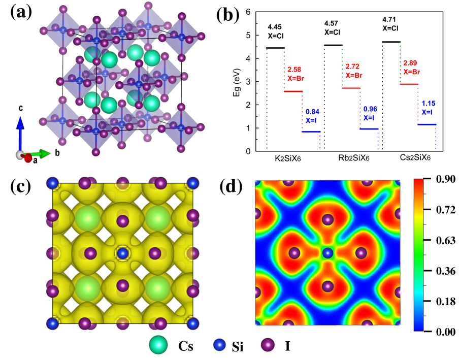
DP is a defect variant for typical perovskite ABX3 structure such as MAPbI340 . In contrast, for the DP with the general formula A2BX6, half of the octahedral B-sites atoms are missing, generating nearly isolated octahedral [BX] units and presenting as the cubic Fmm phases28 . Represented by Cs2SiI6, the DP structure is shown in Fig. 1(a). We can see that the vacancy-ordered DPs formed by face-centered [SiI] units and A-site Cs cations uniformly occupy the voids outer the octahedrons. In our calculations, structural parameters of a series of optimized A2SiX6 DPs (A=K, Rb, Cs; X=Cl, Br, I) are provided in Table S1 (see Ref. 56 ). It is found that the lattice constants and Si-X bond lengths gradually increase along with the atomic number of A-site cation and X-site anion severally.
Because there are no related studies on Si-based DPs, and HSE06 hybridized functional predicting band gaps of A2B(IV)X6 type compounds are in good agreement with their experimental values, such as Cs2SnI6, Cs2TiI630 ; 41 . Therefore, HSE06 functional is adopted for subsequent electronics and optics investigations.
The band gaps of A2SiX6 (A=K, Rb ,Cs; X=Cl ,Br ,I) DPs are all direct types. Figure 1(b) displays their band gap values, range from 4.71 to 0.84 eV, including three small gaps with I-containing compounds, namely, K2SiI6, Rb2SiI6 and Cs2SiI6, which are 0.84 eV, 0.96 eV and 1.15 eV, respectively. For compounds that have the same A-site cation, the gaps follow a tendency of A2SiCl6 A2SiBr6 A2SiI6 that is consistent with the trend of MAPbI3 (X = Cl, Br ,I) 42 . This trend can be analyzed by the electronegativity and density of electronic states (DOS). We present the charge density of Cs2SiI6 in Fig. 1(c). As shown, the charge density mainly distribute over I atoms, while Si atoms has few, indicating charges transfer from the less electronegative Si to the more electronegative I. The overlap of the orbitals along the bonding axis reveals its bonding type. And taking the DOS of Cs2SiX6 as an example (see Ref. 56 ), valence band edges mainly origin from X atoms, while both X and Si atoms contribute to conduction band edges in three cases. According to Pauling electronegativity43 , halogen atoms have the strength order of I (2.66) Br (2.96) Cl (3.16). The higher electronegativity of X element, the stronger bond interaction between X and Si atoms, thus raising the conduction band and generating larger band gap. Whereas in the same X-site anion situation, the gaps form a tendency of Cs2SiX6 Rb2SiX6 K2SiX6 and the reason will be explored later in detail.
To achieve deeper insight into the bonding nature, we analysed the electron localization function (ELF). The ELF renormalizes the values range from 0.00 to 1.00. And the values of 1.00 and 0.50 characterize fully localized and delocalized electrons, respectively, while 0.00 denotes a very low charge density44 . As displayed in Fig. 1(d), the large red region around I, corresponding to values about 0.90, implies the dominated localized features of valence electrons. Although limbic region of the Si-I bond is in green, it demonstrates weakly delocalized behavior of their high-energy orbital valence electrons.
According to the Shockley-Queisser limit45 , which is utilized to evaluate the theoretical photovoltaic conversion efficiency (PCE) in a single junction solar cell, a superior light absorber should possess a band gap ranging from 1.0 to 1.5 eV so as to idealize the efficiency35 . In tandem devices, the maximum PCE requires a rear cell with a gap of 0.9 to1.2 eV46 . Therefore, we unify the ideal band gap to be in the range of 0.9-1.5 eV. Considering the slight deviation of the band gap of K2SiI6 (0.84eV), we here have screened three candidates, K2SiI6, Rb2SiI6 and Cs2SiI6 (A2SiI6) DPs that can be applied in single or tandem solar cells. Moreover, the spin-orbit coupling (SOC) effect is further considered to correct the band. The corrected values are 0.71 eV, 0.82 eV, and 0.99 eV for K2SiI6, Rb2SiI6, and Cs2SiI6, respectively. These effects on band gaps are much smaller than that of Cs2SnI6 or Cs2TeI6 due to the quite lighter B-site element41 .
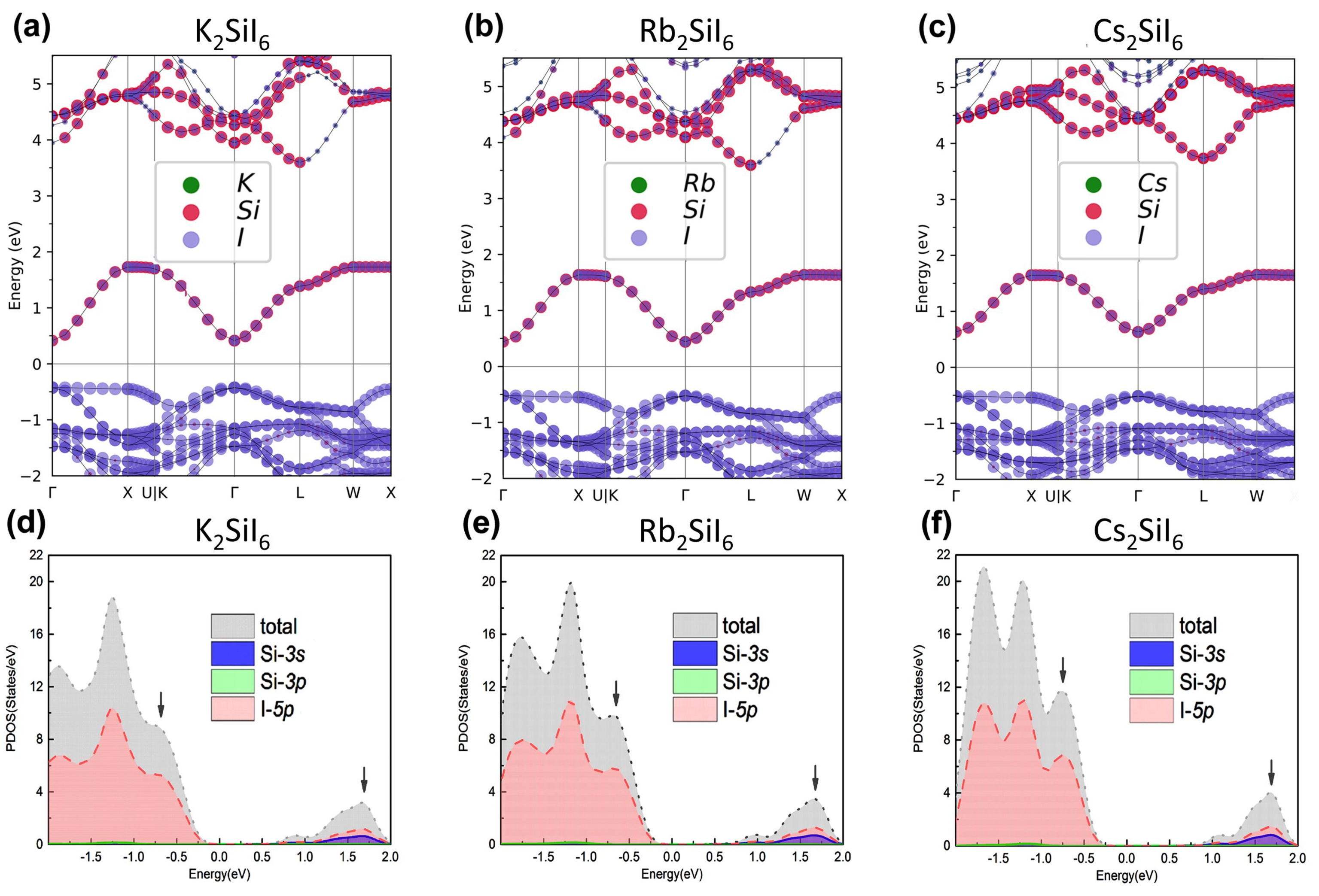
Figure 2(a)-2(c) show the projected band structures of the three promising I-based DPs. We can see that in all three cases, the main components of the band edges are analogous to the situation when the anion are Cl- and Br-. With the A-site elements barely involve in the formation of band edges, the lower conduction bands are dominated by the Si and I elements, and the upper valence bands mostly come from the I elements. Both conduction band minimum (CBM) and valence band maximum (VBM) locate in the points, proving direct band gaps in these A2SiI6 DPs. To visualize the occupied states, Fig. S2(a)-S2(b)56 provide the wave function distribution plots of Cs2SiI6 at VBM and CBM in real space, which can further support our results.
To acquire more band information, we analyze the projected density of electronic states (PDOS) of Si and I atoms near Fermi-level. As shown in Fig. 2(d)-2(f), I-5p and hybridized Si-3s and I-5p orbitals separately constitute the majority of valence and conduction band edges in all three cases. The DOS peaks near the Fermi-level of the three I-based DPs have a significant trend of K2SiI6 Rb2SiI6 Cs2SiI6, indicating the increasing tendency of I-5p bonding states and anti-bonding states between Si-3s and I-5p orbitals, resulting in the band gap trend of K2SiI6 Rb2SiI6 Cs2SiI6.
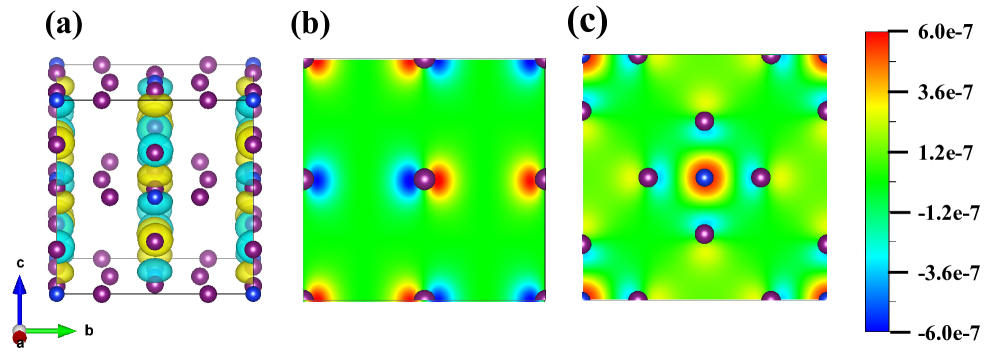
It is noticed that above the Fermi level, there exists a well dispersive and isolated band with a bandwidth of 1.32 eV, 1.20 eV and 1.03 eV for K2SiI6, Rb2SiI6, and Cs2SiI6, respectively [Fig. 2(a)-2(c)]. The wide band dispersion indicates the potential favorable electron mobility. Whereas the dispersion of valence bands is weaker than that above conduction bands, which can be typically illustrated by the wave function distributions at VBM and CBM. Taking Cs2SiI6 as an example, as shown in Fig. 3(a)-3(c), the states of VBM are distributed over partial I atoms, since there are no wave fuction distributions over one third I atoms [Fig. 3(a)]. But the wave fuction of CBM significantly spreads over all Si and I atoms in our observations. Owing to the smaller absolute value of wave function about CBM [Fig. 3(b)-3(c)], the large delocalized traits related to hybrid Si-3s and I-5p states are also observed, producing the more dispersive conduction bands than the upper valence bands near the Fermi level.
The well dispersive band directly reflects the small carrier effective mass. By using Equation1, the carrier effective masses for the K2SiI6, Rb2SiI6 and Cs2SiI6 were calculated around points.
| (1) |
| Compounds | ||
|---|---|---|
| K2SiI6 | 0.17 | -0.53 |
| Rb2SiI6 | 0.18 | -0.56 |
| Cs2SiI6 | 0.23 | -0.63 |
As their dispersive conduction bands states revealed, all three DPs possess small effective electron masses [Table 1], indicating benign conductivity. The heavier hole masses are also in consistence with the prior wave function analysis, reflecting that A2SiI6 DPs are more suitable for n-type semiconductors. The effective masses of all the three A2SiI6 DPs are slightly larger than MAPbI347 , but smaller than other A2B(IV)X6 type compounds, such as Rb2PtI6 and Cs2SnI641 . The electron effective masses of these three DPs have an increasing tendency: K2SiI6 Rb2SiI6 Cs2SiI6, which accords with the dispersion degree of their first conduction bands [Fig. 2(a)-2(c)].
The band structure can directly determine the performance of photon absorption. Then the optical properties of the three A2SiI6 DPs were investigated by calculating the frequency dependent dielectric tensor , where and are the real and imaginary parts in several, and is the photon frequency48 . Utilizing dielectric tensor, the optical absorption coefficient can be obtained by the following Equation2.
| (2) |
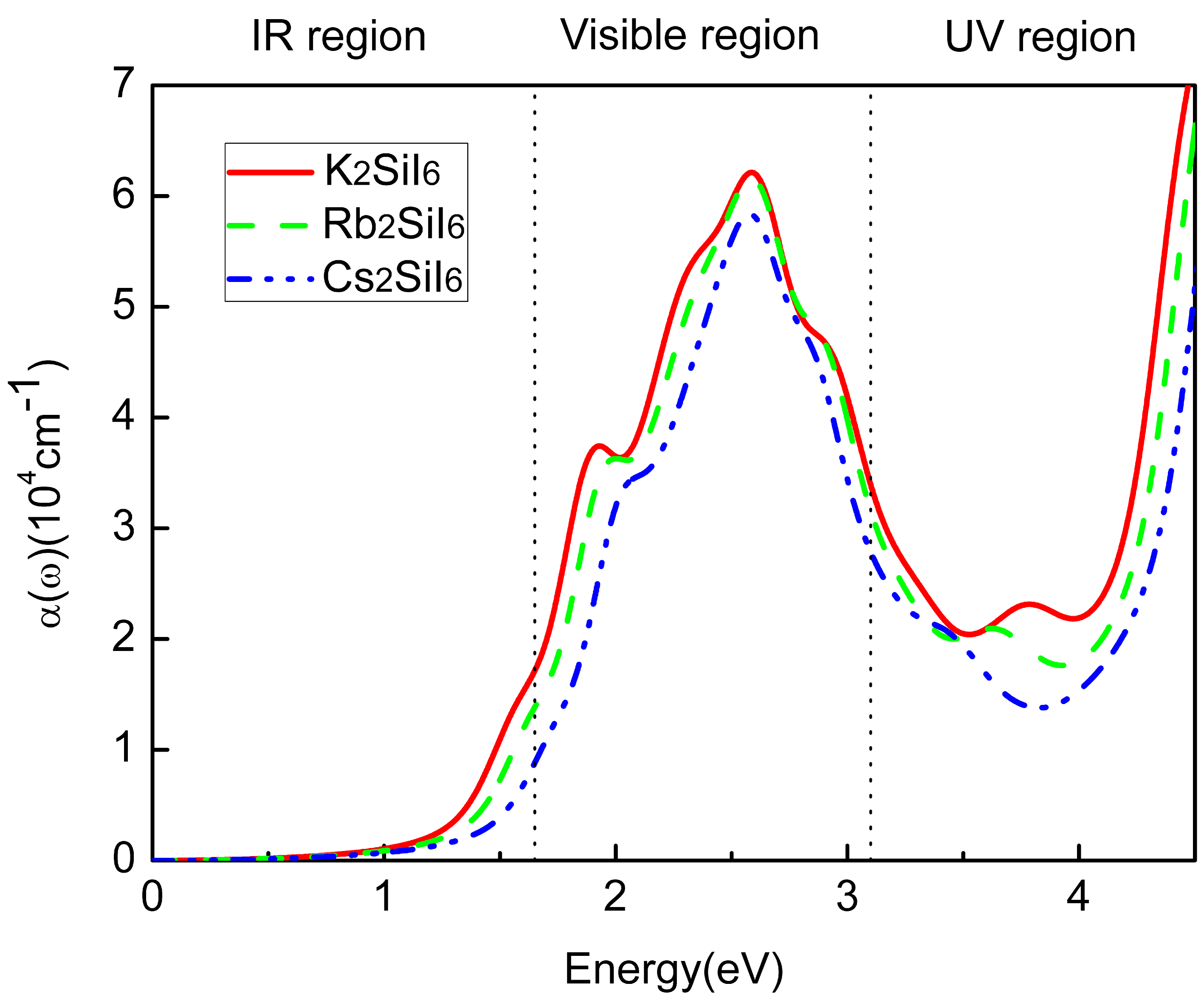
As shown in Fig. 4, the three A2SiI6 DPs happen to exhibit an absorption peak in the visible region. With the increase of band gap, the edges of absorption spectra show a blue shift trend. The absorption ability of these three DPs in visible region follows the trend of K2SiI6 Rb2SiI6 Cs2SiI6 based on absorption peak and band width. The wide absorptions in visible region are associated to their dispersive lower conduction band and band gap. To evaluate the optical absorption capacity of the three DPs, we have calculated as well the photon absorption coefficients of monocrystalline silicon for the sake of comparison. As shown in Fig. S356 , the indirect band gap value of 1.19 eV is consistent with the experimental value of 1.12 eV3 . The absorption peak of A2SiI6 in the visible region is lower than that of Si, but the absorption width is significantly wider. Considering crystalline silicon solar cells have achieved efficiency exceeding 25%3 , the three A2SiI6 DPs seem to be promising lead-free perovskite optical absorption layers.
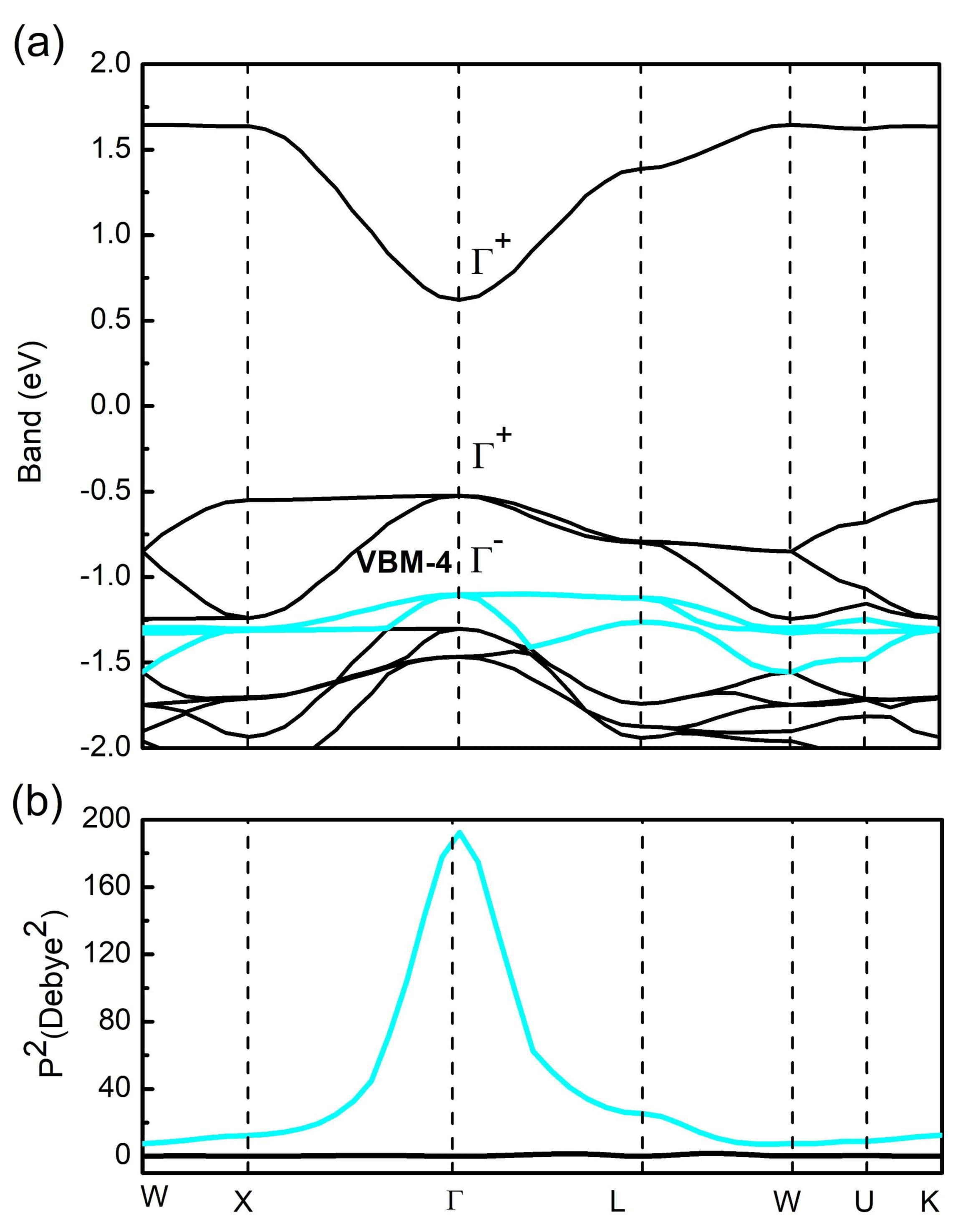
To probe the origin of the strong light-harvesting capability of the above three A2SiI6 DPs, we have analyzed the parity-forbidden transitions via calculating the parity and transition dipole moment between valence bands and the conduction bands of interest. Taking Cs2SiI6 as an example, the VBM at the point exhibits the even parity, possessing a triple degeneracy and the CBM has also even parity [Fig. 5(a)]. Therefore, the transition from VBM to CBM would not occur and finally produces the zero transition matrix elements. The lower three valence bands below the degenerately top three valence bands are also threefold degenerate and thus are denoted as VBM-4. VBM-4 owns the odd parity, indicating the transition from VBM-4 to CBM is allowed. As a result, there is transition dipole moment from VBM-4 to CBM. Our result reveals that the direct transition from VBM to CBM is forbidden and the transition matrix elements are mainly originated from transition between VBM-4 and CBM. The dipole-moment-allowed direct optical transitions of Cs2SiI6, K2SiI6 and Rb2SiI6 are 1.73 eV, 1.57 eV and 1.63 eV, respectively. In general, according to the distributions of transition matrix elements in Fig. 5(b), the three A2SiI6 DPs maintain their absorption characteristics in a wide visible region, suggesting the potential optical absorbers for solar cells. It is worthy to note that K2SiI6 would achieve the best optical performance among the three DPs due to the best optical transition gap of 1.57 eV according to the Shockley-Queisser standard 45 and the optimum optical absorption in the visible region.
Stability is one of the most important part of judging the application potential of materials. Therefore, we calculated the elastic constants to evaluate mechanical stability of the three I-based DPs. For cubic crystal system, the elastic constants satisfy the Born stability criterion , and , manifesting mechanical stability49 . These elastic constants are defined as
| (3) |
Here E is the energy of the crystal, denotes equilibrium volume, and gives a strain. Table 2 lists the elastic constants of the three A2SiI6 DPs. Our results reveal the mechanical stability of the three A2SiI6 DPs, since the Born stability criterion are well matched.
| Compounds | C11(GPa) | C12(GPa) | C44(GPa) | stability |
|---|---|---|---|---|
| K2SiI6 | 13.12 | 3.79 | 5.58 | stable |
| Rb2SiI6 | 12.94 | 8.09 | 8.59 | stable |
| Cs2SiI6 | 10.22 | 5.25 | 5.95 | stable |
We also calculated the decomposition enthalpy () to evaluate the thermodynamical stability. The is defined as
| (4) |
| Compounds | Bader Charge | Mulliken Charge | |||||
|---|---|---|---|---|---|---|---|
| mental | Si | I | mental | Si | I | ||
| K2SiI6 | 41.11 | 0.89 | 1.26 | -0.508 | 0.89 | 0.20 | -0.330 |
| Rb2SiI6 | 75.55 | 0.87 | 1.35 | -0.515 | 0.89 | 0.21 | -0.332 |
| Cs2SiI6 | 68.89 | 0.85 | 1.37 | -0.513 | 0.88 | 0.21 | -0.328 |
The detailed are listed in Table 3. The positive values of the three compounds indicate their thermodynamics stability, of which Rb2SiI6 owns the maximum decomposition energy. The compositional stability can be also demonstrated by the charge transfer between atoms upon its formation. We analyzed the Bader charge and the Mulliken charge50 ; 51 and Table 3 lists the charge transfer of each atom in A2SiI6. It shows that the metal and Si atoms are positively charged and thus can be regarded as electron donors, while iodine is the only electron acceptor upon the formation of system. Focusing on the amount of charge obtained by iodine in all three cases, Rb2SiI6 gains the most electrons in the two cases, indicating the optimum combination stability in the three DPs, which is consistent with the result of decomposition energy. In addition, considering the facts that the Pauling electronegativity of Sn (1.96) is stronger than that of Si (1.90)43 and Cs2SnI6 has been extensively synthesized in experiments28 ; 29 ; 52 ; 53 , so it is believed that the three Si-based DPs have the great feasibility of experimental fabrications.
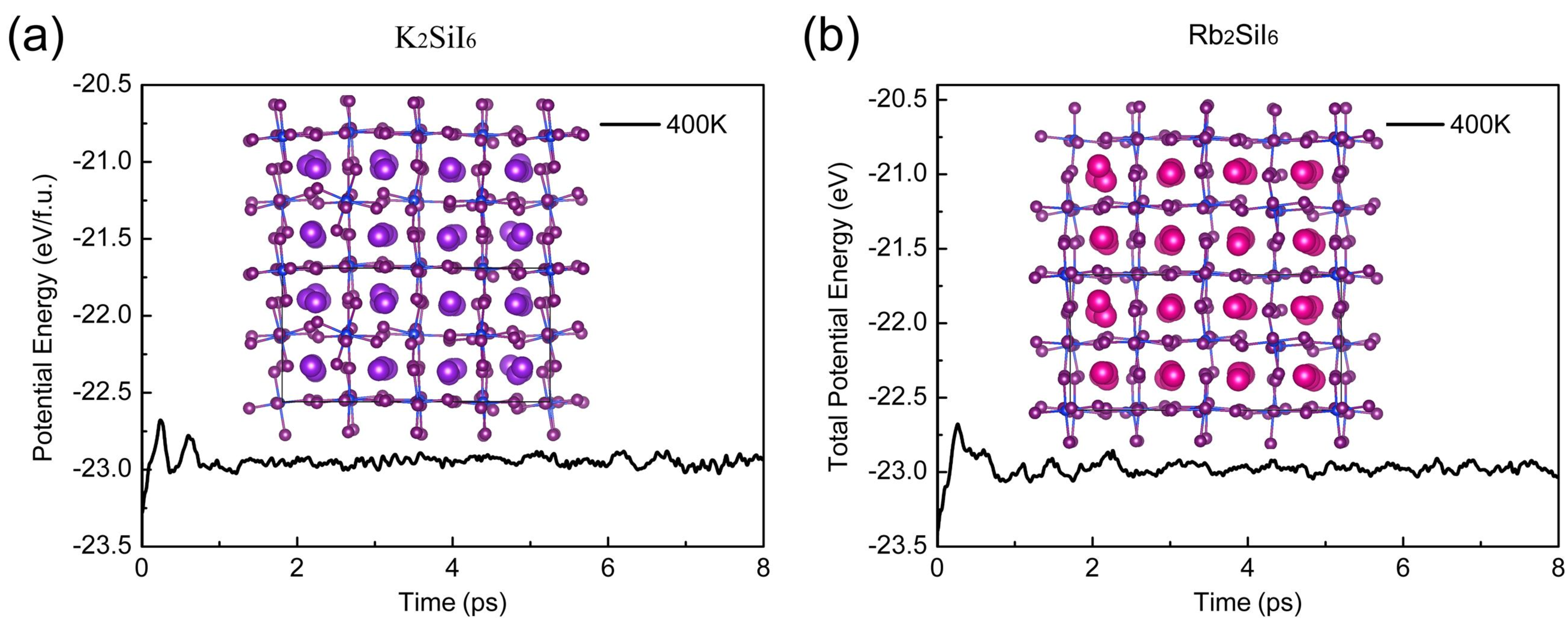
According to international standard (IEC 61646 climatic chamber test), the long-term stability of the 85∘C is required for PSCs. Hence, the molecular dynamics (MD) of the three I-based DPs at the temperature of 400K were simulated. Figure 6 shows the potential energy per formula (f.u.) and the final structures of K2SiI6 and Rb2SiI6, which can be seen that the both potential energy finally converges to a range less than 50 meV/atom, indicating outstanding dynamic stability. The well maintained structures of K2SiI6 and Rb2SiI6 also prove their stabilities. However, Cs2SiI6 was found to be dynamically unstable at 400 K [Fig. S456 ] or at room temperature 300 K, which is similar to Cs2AgBiI654 . So we calculated the integrated crystal orbital Hamilton population (ICOHP) to quantitative description the Si-I bond strength55 . As demonstrated by Table S256 , K2SiI6 has the maximum value of 1.24, meaning the maximum bonding interactions in Si-X bonds within three DPs. While, Cs2SiI6 has the minimum value of 1.21. Therefore, the stability problem of Cs2SiI6 stems from the longer Si-I bonding and the weaker Si-I covalency.
IV Conclusion
Using first-principles calculation, we explored and predicted a new kind of Si-based DPs for photovoltaic applications. The results show K2SiI6, Rb2SiI6 and Cs2SiI6 DPs exhibit excellent electronic, optical and stable properties, such as reasonable band gaps, small carrier effective masses, wide photon absorption in visible range, providing more options for the development of lead-free perovskite optical absorbers. These three DPs are more suitable for n-type semiconductors due to their well dispersive lower conduction bands and smaller electron effective masses. K2SiI6 could achieve the best optical performance in the three DPS due to its best optical transition gap of 1.57 eV and optimum optical absorption in the visible region. According to the comprehensive stability results, Rb2SiI6 has the best stability, followed by K2SiI6. Although Cs2SiI6 has dynamic stability problems, the prospects of the new family of DPs for PCSs are promising.
Acknowledgements.
This work was supported by National Natural Science Foundation of China (No.11904312 and 11904313),the Project of Hebei Educational Department, China(No.ZD2018015 and QN2018012) and the Natural Science Foundation of Hebei Province (No. A2019203507). Thanks to the High Performance Computing Center of Yanshan University.References
- (1) A. Kojima, K. Teshima, Y. Shirai and T. Miyasaka, Organometal Halide Perovskites as Visible-Light Sensitizers for Photovoltaic Cells, J. Am. Chem. Soc. 2009, 131, 6050.
- (2) H.-S. Kim, A. Hagfeldt and N.-G. Park, Morphological and Compositional Progress in Halide Perovskite Solar Cells, Chem. Commun. 2019, 55, 1192.
- (3) C. Battaglia, A. Cuevas and S. De Wolf, High-Efficiency Crystalline Silicon Solar Cells: Status and Perspectives. Electron-Hole Diffusion Lengths Exceeding 1 Micrometer in an Organometal Trihalide Perovskite Absorber, Energy Environ. Sci. 2016, 9, 1552.
- (4) S. D. Stranks, G. E. Eperon, G. Grancini, C. Menelaou, M. J. P. Alcocer, T. Leijtens, L. M. Herz, A. Petrozza and H. J. Snaith, Electron-Hole Diffusion Lengths Exceeding 1 Micrometer in an Organometal Trihalide Perovskite Absorber, Science 2013, 342, 341.
- (5) J. M. Frost, K. T. Butler, F. Brivio, C. H. Hendon, M. van Schilfgaarde and A. Walsh, Atomistic Origins of High-Performance in Hybrid Halide Perovskite Solar Cells, Nano Lett. 2014, 14, 2584.
- (6) P. Umari, E. Mosconi and F. De Angelis, Relativistic GW Calculations on CH3NH3PbI3 and CH3NH3SnI3 Perovskites for Solar Cell Applications, Sci. Rep. 2015, 4, 4467.
- (7) W.-J. Yin, T. Shi and Y. Yan, Unusual Defect Physics in CH3NH3PbI3 Perovskite Solar Cell Absorber, Appl. Phys. Lett. 2014, 104, 063903.
- (8) A. Buin, P. Pietsch, J. Xu, O. Voznyy, A. H. Ip, R. Comin and E. H. Sargent, Materials Processing Routes to Trap-Free Halide Perovskites, Nano Lett. 2014, 14, 6281.
- (9) V. D’Innocenzo, A. R. Srimath Kandada, M. De Bastiani, M. Gandini and A. Petrozza, Tuning the Light Emission Properties by Band Gap Engineering in Hybrid Lead Halide Perovskite, J. Am. Chem. Soc. 2014, 136, 17730.
- (10) A. Filippetti and A. Mattoni, A. Hybrid Perovskites for Photovoltaics: Insights from First Principles, Phys. Rev. B 2014, 89, 125203.
- (11) W. S. Yang, B.-W. Park, E. H. Jung, N. J. Jeon, Y. C. Kim, D. U. Lee, S. S. Shin, J. Seo, E. K. Kim, J. H. Noh and S. I. Seok, Iodide Management in Formamidinium-Lead-Halide-Based Perovskite Layers for Efficient Solar Cells, Science 2017, 356, 1376.
- (12) M. Saliba, T. Matsui, J.-Y. Seo, K. Domanski, J.-P. Correa-Baena, M. K. Nazeeruddin, S. M. Zakeeruddin, W. Tress, A. Abate, A. Hagfeldt and M. Grätzel, Cesium-Containing Triple Cation Perovskite Solar Cells: Improved Stability, Reproducibility and High Efficiency, Energy Environ. Sci. 2016, 9, 1989.
- (13) Y.-C. Hsiao, T. Wu, M. Li, Q. Liu, W. Qin and B. Hu, Fundamental Physics behind High-Efficiency Organo-Metal Halide Perovskite Solar Cells, J. Mater. Chem. A 2015, 3, 15372.
- (14) W. Zhang, G. E. Eperon and H. J. Snaith, Metal Halide Perovskites for Energy Applications, Nat. Energy 2016, 1, 16048.
- (15) F. Zhang, W. Shi, J. Luo, N. Pellet, C. Yi, X. Li, X. Zhao, T. J. S. Dennis, X. Li, S. Wang, Y. Xiao, S. M. Zakeeruddin, D. Bi and M. Grätzel, Isomer-Pure Bis-PCBM-Assisted Crystal Engineering of Perovskite Solar Cells Showing Excellent Efficiency and Stability, Adv. Mater. 2017, 29, 1606806.
- (16) X. Li, D. Bi, C. Yi, J.-D. Dúcoppet, J. Luo, S. M. Zakeeruddin, A. Hagfeldt and M. Grätzel, A Vacuum Flash-Assisted Solution Process for High-Efficiency Large-Area Perovskite Solar Cells, Science 2016, 353, 58-62.
- (17) G. P. Nagabhushana, R. Shivaramaiah and A. Navrotsky, Direct Calorimetric Verification of Thermodynamic Instability of Lead Halide Hybrid Perovskites, Proc. Natl. Acad. Sci. USA 2016, 113, 7717.
- (18) B. Conings, J. Drijkoningen, N. Gauquelin, A. Babayigit, J. D’Haen, L. D’Olieslaeger, A. Ethirajan, J. Verbeeck, J. Manca, E. Mosconi, F. D. Angelis and H.-G. Boyen, Intrinsic Thermal Instability of Methylammonium Lead Trihalide Perovskite, Adv. Energy Mater. 2015, 5, 1500477.
- (19) B. Li, Y. Li, C. Zheng, D. Gao and W. Huang, Advancements in the Stability of Perovskite Solar Cells: Degradation Mechanisms and Improvement Approaches, RSC Adv. 2016, 6, 38079.
- (20) Z. Shi, J. Guo, Y. Chen, Q. Li, Y. Pan, H. Zhang, Y. Xia and W. Huang, Lead-Free Organic-Inorganic Hybrid Perovskites for Photovoltaic Applications: Recent Advances and Perspectives, Adv. Mater. 2017, 29, 1605005.
- (21) W. J. Nimens, S. J. Lefave, L. Flannery, J. Ogle, D.-M. Smilgies, M. T. Kieber-Emmons and L. Whittaker-Brooks, Understanding Hydrogen Bonding Interactions in Crosslinked Methylammonium Lead Iodide Crystals: Towards Reducing Moisture and Light Degradation Pathways, Angew. Chem. Int. Ed. 2019, 58, 13912.
- (22) G. Niu, X. Guo and L. Wang, Review of Recent Progress in Chemical Stability of Perovskite Solar Cells, J. Mater. Chem. A 2015, 3, 8970-8980.
- (23) L. Chu, W. Ahmad, W. Liu, J. Yang, R. Zhang, Y. Sun, J. Yang and X. Li, Lead-Free Halide Double Perovskite Materials: A New Superstar Toward Green and Stable Optoelectronic Applications, Nano-Micro Lett. 2019, 11, 16.
- (24) G. Volonakis, M. R. Filip, A. A. Haghighirad, N. Sakai, B. Wenger, H. J. Snaith and F. Giustino, Lead-Free Halide Double Perovskites via Heterovalent Substitution of Noble Metals, J. Phys. Chem. Lett. 2016, 7, 1254.
- (25) X.-G. Zhao, J.-H. Yang, Y. Fu, D. Yang, Q. Xu, L. Yu, S.-H. Wei and L. Zhang, Design of Lead-Free Inorganic Halide Perovskites for Solar Cells via Cation-Transmutation, J. Am. Chem. Soc. 2017, 139, 2630.
- (26) E. Greul, M. L. Petrus, A. Binek, P. Docampo and T. Bein, Highly Stable, Phase Pure Cs2AgBiBr6 Double Perovskite Thin Films for Optoelectronic Applications, J. Mater. Chem. A 2017, 5, 19972.
- (27) A. H. Slavney, T. Hu, A. M. Lindenberg and H. I. Karunadasa, A Bismuth-Halide Double Perovskite with Long Carrier Recombination Lifetime for Photovoltaic Applications, J. Am. Chem. Soc. 2016, 138, 2138.
- (28) A. E. Maughan, A. M. Ganose, M. M. Bordelon, E. M. Miller, D. O. Scanlon and J. R. Neilson, Defect Tolerance to Intolerance in the Vacancy-Ordered Double Perovskite Semiconductors Cs2SnI6 andCs2TeI6, J. Am. Chem. Soc. 2016, 138, 8453.
- (29) B. Lee, C. C. Stoumpos, N. Zhou, F. Hao, C. Malliakas, C.-Y. Yeh, T. J. Marks, M. G. Kanatzidis and R. P. H. Chang, Air-Stable Molecular Semiconducting Iodosalts for Solar Cell Applications: Cs2SnI6 as a Hole Conductor, J. Am. Chem. Soc. 2014, 136, 15379.
- (30) M.-G. Ju, M. Chen, Y. Zhou, H. F. Garces, J. Dai, L. Ma, N. P. Padture and X. C. Zeng, Earth-Abundant Nontoxic Titanium (IV)-Based Vacancy-Ordered Double Perovskite Halides with Tunable 1.0 to 1.8 eV Bandgaps for Photovoltaic Applications, ACS Energy Lett. 2018, 3, 297.
- (31) G. Kresse and J. Furthmüller, Efficient Iterative Schemes for Ab Initio Total-Energy Calculations Using a Plane-Wave Basis Set, Phys. Rev. B 1996, 54, 11169.
- (32) P. E. Blöchl, Projector Augmented-Wave Method, Phys. Rev. B 1994, 50, 17953.
- (33) J. P. Perdew and Y. Wang, Accurate and Simple Analytic Representation of the Electron-Gas Correlation Energy, Phys. Rev. B 1992, 45, 13244.
- (34) J. P. Perdew, K. Burke and Y. Wang, Generalized Gradient Approximation for the Exchange-Correlation Hole of a Many-Electron System, Phys. Rev. B 1996, 54, 16533.
- (35) J. P. Perdew, A. Ruzsinszky, G. I. Csonka, O. A. Vydrov, G. E. Scuseria, L. A. Constantin, X. Zhou and K. Burke, Restoring the Density-Gradient Expansion for Exchange in Solids and Surfaces, Phys. Rev. Lett. 2008, 100, 136406.
- (36) J. Heyd, G. E. Scuseria and M. Ernzerhof, Hybrid Functionals Based on a Screened Coulomb Potential, J. Chem. Phys. 2003, 118, 8207.
- (37) H. J. Monkhorst and J. D. Pack, Special Points for Brillouin-Zone Integrations, Phys. Rev. B 1976, 13, 5188-5192.
- (38) V. Wang, N. Xu, J. C. Liu, G. Tang and W.-T. Geng, VASPKIT: A Pre- and Post-Processing Program for VASP Code, arXiv:1908.08269 [cond-mat].
- (39) S. Maintz, V. L. Deringer, A. L. Tchougréeff and R. Dronskowski, LOBSTER: A Tool to Extract Chemical Bonding from Plane-Wave Based DFT: Tool to Extract Chemical Bonding, J. Comput. Chem. 2016, 37, 1030.
- (40) A. Poglitsch and D. Weber, Dynamic Disorder in Methylammoniumtrihalogenoplumbates (II) Observed by Millimeter-wave Spectroscopy, J. Chem. Phys. 1987, 87, 6373.
- (41) See Supplemental Material at http://link.aps.org/supplemental/10.1103/PhysRevX.XXXXX for optimized lattice constants, local density of states, wave function distributions of VBM and CBM related to Cs2SiI6, optical absorption spectra of Si, simulated MD potential energy of Cs2SiI6 and average ICOHP of Si-I bonds.
- (42) Y. Cai, W. Xie, H. Ding, Y. Chen, K. Thirumal, L. H. Wong, N. Mathews, S. G. Mhaisalkar, M. Sherburne and M. Asta, Computational Study of Halide Perovskite-Derived A2BX6 Inorganic Compounds: Chemical Trends in Electronic Structure and Structural Stability, Chem. Mater. 2017, 29, 7740.
- (43) M.-G. Ju, J. Dai, L. Ma and X. C. Zeng, Perovskite Chalcogenides with Optimal Bandgap and Desired Optical Absorption for Photovoltaic Devices, Adv. Energy Mater. 2017, 7, 1700216.
- (44) L. Pauling, Cornell university press Ithaca, NY., 1960, 260, 3175. The Nature of the Chemical Bond.
- (45) S. Zhang, Q. Wang, Y. Kawazoe and P. Jena, Three-Dimensional Metallic Boron Nitride, J. Am. Chem. Soc. 2013, 135, 18216.
- (46) W. Shockley and H. J. Queisser, Detailed Balance Limit of Efficiency of P-n Junction Solar Cells, J. Appl. Phys. 1961, 32, 510.
- (47) G. E. Eperon, T. Leijtens, K. A. Bush, R. Prasanna, T. Green, J. T.-W. Wang, D. P. McMeekin, G. Volonakis, R. L. Milot, R. May, A. Palmstrom, D. J. Slotcavage, R. A. Belisle, J. B. Patel, E. S. Parrott, R. J. Sutton, W. Ma, F. Moghadam, B. Conings, A. Babayigit, H.-G. Boyen, S. Bent, F. Giustino, L. M. Herz, M. B. Johnston, M. D. McGehee and H. J. Snaith, Perovskite-Perovskite Tandem Photovoltaics with Optimized Band Gaps, Science 2016, 354, 861.
- (48) P.-P. Sun, Q.-S. Li, L.-N. Yang and Z.-S. Li, Theoretical Insights into a Potential Lead-Free Hybrid Perovskite: Substituting Pb2+ with Ge2+, Nanoscale 2016, 8, 1503.
- (49) M. Gajdoš, K. Hummer, G. Kresse, J. Furthmüller and F. Bechstedt, Linear Optical Properties in the Projector-Augmented Wave Methodology, Phys. Rev. B 2006, 73, 045112.
- (50) F. Mouhat and F.-X. Coudert, Necessary and Sufficient Elastic Stability Conditions in Various Crystal Systems, Phys. Rev. B 2014, 90, 224104.
- (51) C. Ertural, S. Steinberg and R. Dronskowski, Development of a Robust Tool to Extract Mulliken and Löwdin Charges from Plane Waves and Its Application to Solid-State Materials, RSC Adv. 2019, 9, 29821.
- (52) W. Tang, E. Sanville and G. Henkelman, A Grid-Based Bader Analysis Algorithm without Lattice Bias, J. Phys.: Condens. Matter 2009, 21, 084204.
- (53) B. Lee, A. Krenselewski, S. I. Baik, D. N. Seidman and R. P. H. Chang, Solution Processing of Air-Stable Molecular Semiconducting Iodosalts, Cs2SnI6−xBr, for Potential Solar Cell Applications, Sustain, Energy Fuels 2017, 1, 710-724.
- (54) W. Zhu, G. Xin, Y. Wang, X. Min, T. Yao, W. Xu, M. Fang, S. Shi, J. Shi and J. Lian, Tunable Optical Properties and Stability of Lead Free All Inorganic Perovskites (Cs2SnIxCl6-x), J. Mater. Chem. A 2018, 6, 2577.
- (55) C. N. Savory, A. Walsh and D. O. Scanlon, Can Pb-Free Halide Double Perovskites Support High-Efficiency Solar Cells? ACS Energy Lett. 2016, 1, 949.
- (56) V. L. Deringer, A. L. Tchougréeff and R. Dronskowski, Crystal Orbital Hamilton Population (COHP) Analysis as Projected from Plane-Wave Basis Sets, J. Phys. Chem. A 2011, 115, 5461.