Preparing single SiV- center in nanodiamonds for external, optical coupling with access to all degrees of freedom
Supplemental Material for "Preparing single SiV- center in nanodiamonds for external, optical coupling with access to all degrees of freedom"
Abstract
Optical coupling enables intermediate- and long-range interactions between distant quantum emitters. Such interaction may be the basic element in bottom-up approaches of coupled spin systems or for integrated quantum photonics and quantum plasmonics. Here, we prepare nanodiamonds carrying single, negatively-charged silicon-vacancy centers for evanescent optical coupling with access to all degrees of freedom by means of atomic force nanomanipulation. The color centers feature excellent optical properties, comparable to silicon-vacancy centers in bulk diamond, resulting in a resolvable fine structure splitting, a linewidth close to the Fourier-Transform limit under resonant excitation and a good polarization contrast. We determine the orbital relaxation time of the orbitally split ground states and show that all optical properties are conserved during translational nanomanipulation. Furthermore, we demonstrate the rotation of the nanodiamonds. In contrast to the translational operation, the rotation leads to a change in polarization contrast. We utilize the change in polarization contrast before and after nanomanipulation to determine the rotation angle. Finally, we evaluate the likelihood for indistinguishable, single photon emission of silicon-vacancy centers located in different nanodiamonds. Our work enables ideal evanescent, optical coupling of distant nanodiamonds containing silicon-vacancy centers with applications in the realization of quantum networks, quantum repeaters or complex quantum systems.
-
October 2019
Keywords: nanodiamonds, color centers in diamond, silicon-vacancy center, quantum optics, hybrid quantum systems
1 Introduction
Color centers in diamond promise to be the key element for upcoming quantum technologies such as quantum networks [1] or quantum sensors [2, 3]. The most studied color center so far is the negatively-charged nitrogen-vacancy (NV-) center, due to its outstanding spin properties and magnetic field sensitivity [4, 5]. For many applications, color centers close to the diamond surface are mandatory to allow efficient coupling to objects outside the diamond host. A special case are nanodiamonds (NDs), with dimensions small compared to the optical wavelength which, since recently, are also fabricated with high quality in top-down approaches [6]. In such cases, color centers inside the ND can be efficiently coupled to the outside optically via the evanescent field. Optical coupling gives access to, for example, post-processing of classical photonics towards quantum photonics applications [7, 8, 9, 10].
For efficient operation, it is important to optimize all degrees of freedom such as position, dipole alignment as well as the intrinsic optical properties, like a high flux of coherent photons, spectral stability and a narrow inhomogeneous distribution. The NDs offer the unique capability to optimize all degrees of freedom by means of atomic force microscope (AFM)-based nanomanipulation. In order to obtain an optimal evanescent coupling to an object outside the ND three basic operations are required. First, a high-precision translational manipulation [11]. Second, a high-precision rotational manipulation [12]. In case of NV- centers, the rotation angle was determined with respect to an external field by monitoring the change in ODMR signal. Third, the maintenance of ideal intrinsic properties. For optical coupling crucial intrinsic properties of the defect center include narrow homogeneous and inhomogeneous linewidths, good polarization contrast, low-background single photon emission and the ability of indistinguishable photon emission. The intrinsic properties remain a major drawback for NV- centers in NDs due to the degradation of the optical and spin properties when the NV- center is located in close proximity to the diamond surface.
In contrast, the negatively-charged silicon-vacancy (SiV-) center has drawn great attention due to its robust intrinsic properties. In bulk diamond SiV- centers show exceptional optical properties [13, 14, 15], with a high Debye-Waller factor of [16], a narrow inhomogeneous linewidth in the range of few GHz and Fourier-Transform limited homogeneous linewidth at cryogenic temperatures [17]. The spectral stability arises from the symmetry of the SiV- center and enables to achieve excellent optical properties even in close proximity to the diamond surface. Protecting the high-degree of symmetry demands high quality of the diamond host, in particular, a low strain environment. In chemical vapour deposition (CVD) NDs single photon emission from SiV- centers [18] and photostable quantum emitters with sub-gigahertz linewidth [19] were shown. The production of low-strain nanodiamonds via HPHT fabrication method [12, 20] recently enabled to preserve the excellent optical properties of SiV- centers also in NDs. In NDs with high crystal quality and sizes smaller than an inhomogeneous distribution of at and individual lines narrower than were found [21]. Utilizing plasma treatment techniques of the diamond surface SiV- centers with an inhomogeneous ensemble linewidth below the excited state splitting and excellent spectral stability under resonant excitation was achieved [12]. While the requirement to maintain ideal intrinsic properties also in NDs has been shown the demonstration of nanomanipulation of NDs containing single SiV- centers is still missing. The translational nanomanipulation is a straightforward extension of the work done with NV- centers [11, 12], but the rotational operation needs further developments. The determination of the rotation angle via ODMR contrast with respect to an external field, as done with NV- centers [12], is not possible with SiV- centers. Furthermore, an open question remains on the fragility of the intrinsic properties on the nanomanipulation process. For example, conserving the intrinsic properties of the color centers during nanomanipulation on the NDs is crucial to enable the deterministic coupling of NDs with incorporated color centers with preselected properties, for example, in quantum photonics applications.
In this work we develop and test the complete post-processing procedure. We first isolate single SiV- centers in single ND, characterize the optical properties and choose the once with preferred optical properties comparable to SiV- centers in low-strain bulk diamond. We then perform the nanomanipulation operations, in particular translational and rotational operation needed for the post-processing step. Finally, we characterize the optical properties of the same SiV- centers again after nanomanipulation was performed and explicitly show that the optical properties of the color centers are conserved. The nanomanipulation enables optimization on all degrees of freedom of NDs hosting SiV- centers with an AFM cantilever. In addition we show that ND decomposition leads to a change in strain indicated by a change of the fine structure splitting. Finally, we proof the ability for indistinguishable, single photon emission from SiV- centers in different NDs.
2 Methods
Measurements presented in this manuscript were performed using a custom-built cryogenic confocal microscope. It consists of a compact design flow cryostat to cool down the sample to liquid helium temperature, a microscope objective and a pinhole to achieve sub micrometer depth resolution. A dual-axis scanning galvo system is used to scan the sample surface, which is mounted on the cold finger of the cryostat. Off-resonant excitation of the color centers is done with a green DPSS laser at , while for resonant excitation we use a tunable diode laser at . The fluorescence of the SiV- centers is collected with the microscope objective and analyzed either using a single photon counting module (SPCM) or a grating spectrometer with a grating.
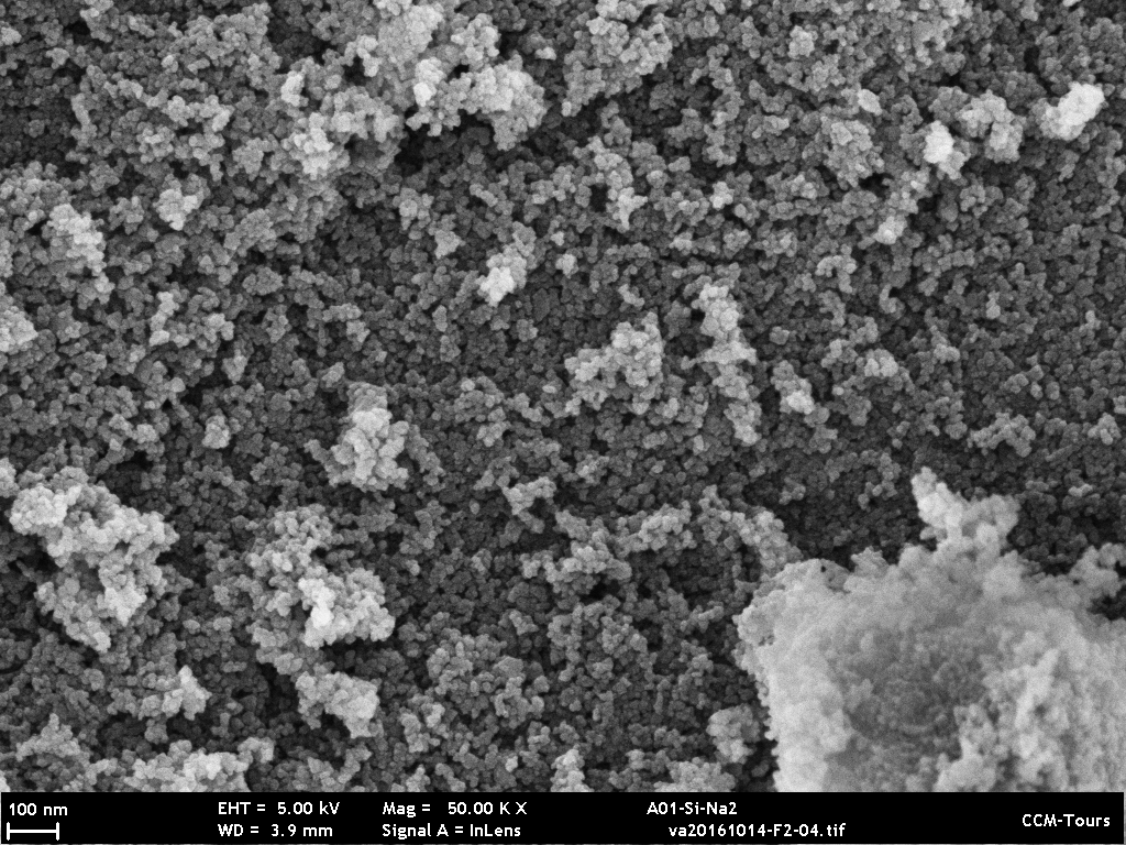
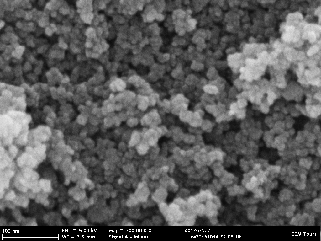
NDs with SiV- color centers were obtained by high pressure – high temperature (HPHT) treatment of the catalyst metals-free hydrocarbon growth system based on homogeneous mixtures of naphthalene - (Chemapol) and tetrakis(trimethylsilyl)sylane – (Stream Chemicals Co.), which was used as the doping component. Cold pressed tablets of the initial mixture ( diameter and height) were placed into a graphite container, which simultaneously served as a heater of the high-pressure toroid-type apparatus. The experimental procedure consisted of loading the high-pressure apparatus to at room temperature, heating the sample to the temperature of diamond formation (), and short () isothermal exposure at this temperature. The recovered diamond materials have been characterized under ambient conditions by using X-ray diffraction, Raman spectroscopy and scanning and transmission electron microscopes (SEM and TEM). SEM images of the diamond nanoparticles can be found in the Supplemental Material. According to this characterization, diamond material, mainly, represent agglomerations relatively uniform nanoparticles that are in size. In addition, samples may contain a small amount of larger fractions of diamond, which are formed in a narrow zone of direct contact of the original mixture with the inner surface of the graphite heater, corresponding to the area of maximum temperatures in the high-pressure apparatus.
The NDs were spin coated on a type-IIa-diamond substrate to ensure good thermal conductivity. After spin coating of the ND solution some of the NDs tend to cluster. A repeated deagglomeration could be achieved using an AFM cantilever as it is described in section 4. For better orientation the substrate is provided with a variety of markers that were produced by focused ion beam milling.
3 Isolating single SiV- centers
The NDs occupy a low concentration of SiV- center potentially enabling to isolate single SiV- centers per one ND or cluster of NDs. In figure 1(a) a confocal image of a area of the sample with several fluorescing spots is shown. Few of them show a four-line structure which corresponds to the four optical transitions (A-D) of the SiV- center zero-phonon line (ZPL) visible with off-resonant () excitation (c.f. figure 1(b)). The splitting of the electronic ground state () and excited state () is hereby caused by spin-orbit interaction. An exemplary low temperature photoluminescence (PL) spectrum of a SiV- center in a ND with its ZPL centered at is shown in figure 1(c). A resolvable fine structure of single SiV- centers already indicates a high crystal quality and low strain of the NDs. The PL linewidth of the individual lines in figure 1(c) is limited by the resolution of the grating spectrometer to about .
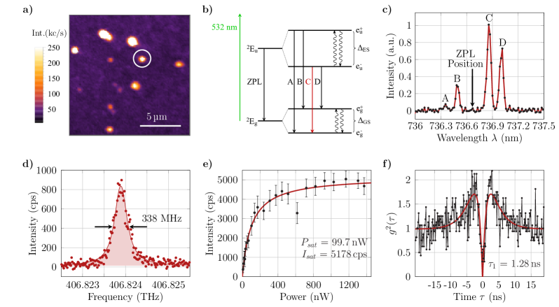
Determination of the homogeneous linewidth of an individual SiV- center is done via photoluminescence excitation (PLE) spectroscopy (figure 1(d)). We hereby scan the frequency of a resonant laser over transition C and record the fluorescence of the phonon sideband (PSB) using a bandpass filter. We measure a linewidth of under resonant excitation, about 3 times broader than the natural linewidth of SiV- that was reported in bulk diamond [17]. The broadening mainly arises from residual spectral diffusion. For the same ND we measure the powerdependence of the fluorescence under resonant excitation and fit a saturation curve following the model
| (1) |
to the data (figure 1(e)) yielding and . In a second-order autocorrelation measurement (figure 1(f)) we find a value well below which implies that we indeed address a single SiV- center.
In the following we assume that we are investigating NDs containing a single SiV- center if three criteria are fulfilled. First, a well isolated fluorescent spot in confocal imaging. Second, a clear four-line structure in PL spectroscopy without any additional lines originating from a second SiV- center. Third, a single, Lorentzian-shaped PLE line scan under resonant excitation.
4 Translational nanomanipulation
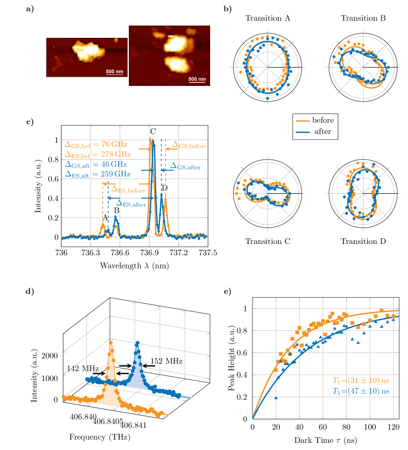
In the following experiments we investigate the change of the optical properties of a ND containing a single SiV- center when it is moved with the cantilever of an AFM. An AFM image of the ND before and after the displacement is shown in figure 2(a).
Apparently from the size of the structure on the AFM image we conclude that we investigate a cluster of NDs. During the nanomanipulation the cluster is split in two parts and shifted on the substrate. The image quality of the second (shifted) image has significantly decreased due to a degeneration of the AFM cantilever when using the contact mode for the displacement of the ND.
We measure the emission polarization of the four optical transitions of the SiV - center (c.f. figure 1(b)) at cryogenic temperatures before and after the nanomanipulation (see figure 2(b)). The lines A and D are perpendicular polarized compared to the lines B and C, which is known as the typical behavior of the SiV- center [14]. The polarization contrast as well as the dipole angle of the individual transitions stay unchanged after the displacement of the ND. We interpret this result as a translational movement without any rotation of the ND. The overall low polarization contrast can be explained by two main reasons. First, the polarization contrast of the individual lines highly depends on the orientation of the ND. For the A and D line, which can be described by a linear combination of X’ and Y’ dipoles (c.f. reference [14]), the polarization contrast changes if the ND is rotated around an angle with respect to the optical axis of the microscope objective (details see Supplemental Material). Second, the maximum polarization contrast is limited by the radiation characteristic of the SiV- center situated in the high refractive index ND into vacuum (n = 1). For a parallel (to the surface) oriented dipole the polarization contrast would be 1 while a perpendicular oriented dipole shows no polarization contrast.
We further investigate the ND properties before and after nanomanipulation via PL and PLE spectroscopy. The PL spectrum (figure 2(c)) shows the four line structure of the SiV- ZPL at . After the displacement of the ND we observe a change of the ground state splitting between the transitions A and B (C and D) from to and of the excited state splitting , which corresponds to the frequency difference between the transitions A and C (B and D), from to . This can be explained by a decrease of the transverse strain when the ND is declustered. The splittings after the nanomanipulation are within the errorbars of the zero-strain splittings of and reported in reference [12]. The absolute line position of the ZPL stays unchanged, which we conclude with no additionally introduced longitudinal strain.
Resonant excitation of transition C before the nanomanipulation yields a linewidth of at an excitation power of , which is close to the Fourier-Transform limit of a SiV- center in bulk diamond [17]. Repeating the measurement after the nanomanipulation yields a linewidth of . In figure 2(d) both, the PLE scan before and after the ND was manipulated is shown.
Additionally, we measure the orbital relaxation time of the ground state via resonant laser pulses on transition C. During each laser pulse the fluorescence decays to a steady state level as the population is pumped to the other ground state by the resonant laser. The respective peak height depends on the dark time between the laser pulses. We compare the peak height of each pulse with the peak height of the first pulse and fit an exponential of the form
| (2) |
to the data, resulting in a time of () before (after) the nanomanipulation. The peak height data together with the exponential fit is depicted in figure 2(e). A slight increase of the time can be related to a better thermal conductivity after the displacement, which leads to a lower temperature of the ND and a longer orbital time of the SiV- center [22].
5 Rotational nanomanipulation
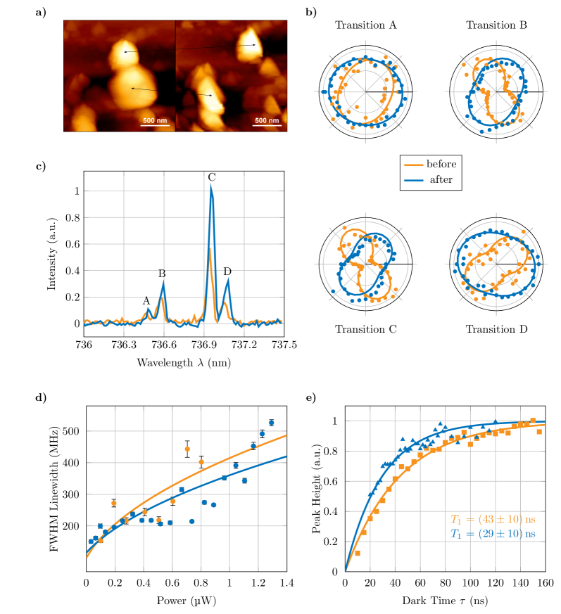
Next, we demonstrate the rotation of a ND again using the AFM cantilever. An AFM image of the ND before and after the displacement is shown in figure 3(a). The ND is laterally displaced by between the two images.
The rotation of the ND is verified by polarization measurements at cryogenic temperatures before and after the nanomanipulation (see figure 3(b)).
From the rotation of the polarization axes of the transitions B and C during the nanomanipulation we extract the rotation of the ND in the x-y-plane, which is for the investigated ND. Further we calculate the rotation of the ND around the angle via the change of the polarization contrast, which in our specific case is (details see Supplemental Material).
Beside the rotation of the polarization angle the optical properties of the SiV- center stay unchanged. A PL spectrum of the ND at cryogenic temperatures before and after the nanomanipulation is shown in figure 3(c). We determine the ground state splitting of the SiV- center to () and the excited state splitting to () before (after) the nanomanipulation. This implies again a low strained ND, which holds true during the rotation. The overall brightness of the center has increased after the nanomanipulation due to better alignment of the SiV- dipole with the optical axis of the laboratory frame.
A comparison of the power-dependence of the PLE linewidth of transition C before and after the nanomanipulation is depicted in figure 3(d). We again measure a narrowest linewidth close to the Fourier-Transform limit being before and after the nanomanipulation. The power broadening of the line is described by a model of the form
| (3) |
where is the Rabi Frequency, is the natural linewidth and is the beam diameter (see reference [23]). The behavior changes slightly during the rotation of the ND due to the change of the dipole alignment.
The measurement of the orbital relaxation time yields before and after the nanomanipulation, agreeing within the error margins. Both the measurement data and the exponential fit according to equation (2) is shown in figure 3(e).
6 Discussion and Conclusion
Summarizing, we have tested the complete post-processing procedure where one and the same SiV- center in a ND was pre-characterized, then nanomanipulation tools were applied on the ND host and finally the same SiV- center was characterized again. We have explicitly proven that the intrinsic properties of single SiV- centers with bulk-like optical properties persist against translational and rotational nanomanipulation of the ND host. Our work gives access to optical coupling of individual, pre-selected SiV- centers in NDs optimizing all degrees of freedom of the coupling term. In total we measured the ZPL position and linewidth (transition C) of 25 SiV- centers (figure 4(a)).

We show significant spectral overlap of several SiV- centers in our NDs. 7 SiV- centers are promising candidates for a Hong-Ou-Mandel interference experiment as they could be assigned to a partner SiV- center with a detuning of the ZPL frequency smaller than the Fourier-Transform limited linewidth (red bars in figure 4(a)). A zoom-in at 5 SiV- centers with an emission frequency of in figure 4(b) already demonstrates a small cluster with significant spectral overlap. Another cluster of 3 SiV- centers emits at (figure 4(b), right). In summary we find an inhomogeneous line distribution of of the 25 investigated SiV- centers (c.f. figure 4(c)), again indicating very low strain in our NDs.
With our results bottom-up approaches of coupled arrays of NDs with incorporated SiV- centers become feasible featuring the realization of quantum simulators. The deterministic coupling to photonic channels enables the construction of large-scale, distributed quantum networks. Also, magnetic field sensing at cryogenic temperatures could profit from well-controlled alignment of all degrees of freedom.
Author Contributions
SH, LH and AK performed the spectroscopic measurements. AFM measurements and nanomanipulation were performed by KGF. LFK, VAD and VNA synthesized the nanodiamonds with SiV- centers. The manuscript was written by SH, LH and AK and all authors discussed the results and contributed to the manuscript.
Acknowledgement
The project was funded by the Deutsche Forschungsgemeinschaft (DFG, German Research Foundation) - Project number: 398628099. AK acknowledges support of the Carl-Zeiss Foundation, BMBF/VDI in project Q.Link.X and the Wissenschaftler-Rückkehrprogramm GSO/CZS. SH and AK acknowledge support of IQst. VAD and LFK acknowledge financial support of the Russian Foundation for Basic Research (Grant 18-03-00936). FJ acknowledges support from EU ASTERIQS (820394), the DFG (JE 290/18-1 and SFB 1279), BMBF/VDI in project Q.Link.X and ERC (BioQ 319130). We thank Gregor Neusser, Christine Kranz and the FIB Center UUlm for etching the markers into the type-IIa-diamond substrate. Experiments performed for this work were operated using the Qudi software suite [24].
References
References
- [1] Stephanie Wehner, David Elkouss, and Ronald Hanson. Quantum internet: A vision for the road ahead. Science, 362(6412), 2018.
- [2] Jeronimo R. Maze, Paul L. Stanwix, James S. Hodges, Seungpyo Hong, Jacob M. Taylor, Paola Cappellaro, Liang Jiang, Gurudev M. V. Dutt, Emre Togan, Alexander Zibrov, Amir Yacoby, Ronald L. Walsworth, and Mikhail D. Lukin. Nanoscale magnetic sensing with an individual electronic spin in diamond. Nature, 455:644–647, 2008.
- [3] Gopalakrishnan Balasubramanian, Ignatius Y. Chan, Roman Kolesov, Mohannad Al-Hmoud, Julia Tisler, Chang Shin, Changdong Kim, Aleksander Wojcik, Philip R. Hemmer, Anke Krueger, Tobias Hanke, Alfred Leitenstorfer, Rudolf Bratschitsch, Fedor Jelezko, and Jörg Wrachtrup. Nanoscale imaging magnetometry with diamond spins under ambient conditions. Nature, 455:648–651, 2008.
- [4] Fedor Jelezko and Jörg Wrachtrup. Single defect centres in diamond: A review. Physica Status Solidi a, 203(13):3207–3225, 2006.
- [5] Marcus W. Doherty, Neil B. Manson, Paul Delaney, Fedor Jelezko, Jörg Wrachtrup, and Lloyd C. L. Hollenberg. The nitrogen-vacancy colour centre in diamond. Physics Reports, 528:1–45, 2013.
- [6] Jiabao Zheng, Benjamin Lienhard, Gregory Doerk, Mircea Cotlet, Eric Bersin, Harrison S. Kim, Young-Chul Byun, Chang-Yong Nam, Jiyoung Kim, Charles T. Black, and Dirk Englund. Top-down fabrication of high-uniformity nanodiamonds by self-assembled block copolymer masks. Scientific Reports, 9(6914), 2019.
- [7] Konstantin G. Fehler, Anna P. Ovvyan, Nico Gruhler, Wolfram H. P. Pernice, and Alexander Kubanek. Efficient coupling of an ensemble of nitrogen vacancy center to the mode of a high-q, si3n4 photonic crystal cavity. ACS Nano, 13(6):6891–6898, 2019.
- [8] Florian Böhm, Niko Nikolay, Christoph Pyrlik, Jan Schlegel, Andreas Thies, Andreas Wicht, Günther Tränkle, and Oliver Benson. On-chip integration of single solid-state quantum emitters with a sio2 photonic platform. New Journal of Physics, 21(4):045007, 2019.
- [9] Tim Schröder, Sara L. Mouradian, Jiabao Zheng, Matthew E. Trusheim, Michael Walsh, Edward H. Chen, Luozhou Li, Igal Bayn, and Dirk Englund. Quantum nanophotonics in diamond. Journal of the Optical Society of America B, 33:B65–B83, 2016.
- [10] Julia Benedikter, Hanno Kaupp, Thomas Hümmer, Yuejiang Liang, Alexander Bommer, Christoph Becher, Anke Krueger, Jason Smith, Theodor W. Hänsch, and David Hunger. Cavity-enhanced single-photon source based on the silicon-vacancy center in diamond. Physical Review Applied, 7:024031, 2017.
- [11] Andreas W. Schell, Günter Kewes, Tim Schröder, Janik Wolters, Thomas Aichele, and Oliver Benson. A scanning probe-based pick-and-place procedure for assembly of integrated quantum optical hybrid devices. Review of Scientific Instruments, 82(7):073709, 2011.
- [12] Lachlan J. Rogers, Ou Wang, Liu Yan, Lukas Antoniuk, Christian Osterkamp, Valery A. Davydov, Viatcheslav N. Agafonov, Andrea B. Filipovski, Fedor Jelezko, and Alexander Kubanek. Single siv- centers in low-strain nanodiamonds with bulklike spectral properties and nanomanipulation capabilities. Physical Review Applied, 11:024073, 2019.
- [13] Christian Hepp, Tina Müller, Victor Waselowski, Jonas N. Becker, Benjamin Pingault, Hadwig Sternschulte, Doris Steinmüller-Nethl, Adam Gali, Jeronimo R. Maze, Mete Atatüre, and Christoph Becher. Electronic structure of the silicon vacancy color center in diamond. Physical Review Letters, 112:036405, 2014.
- [14] Lachlan J. Rogers, Kay D. Jahnke, Marcus W. Doherty, Andreas Dietrich, Liam P. McGuinness, Christoph Müller, Tokuyuki Teraji, Hitoshi Sumiya, Junichi Isoya, Neil B. Manson, and Fedor Jelezko. Electronic structure of the negatively charged silicon-vacancy center in diamond. Physical Review B, 89:235101, 2014.
- [15] Alp Sipahigil, Kay D. Jahnke, Lachlan J. Rogers, Tokuyuki Teraji, Junichi Isoya, Alexander S. Zibrov, Fedor Jelezko, and Mikhail D. Lukin. Indistinguishable photons from separated silicon-vacancy centers in diamond. Physical Review Letters, 113:113602, 2014.
- [16] Andreas Dietrich, Kay D. Jahnke, Jan M. Binder, Tokuyuki Teraji, Junichi Isoya, Lachlan J. Rogers, and Fedor Jelezko. Isotopically varying spectral features of silicon-vacancy in diamond. New Journal of Physics, 16(11):113019, 2014.
- [17] Lachlan J. Rogers, Kay D. Jahnke, Tokuyuki Teraji, Luca Marseglia, Christoph Müller, Boris Naydenov, Hardy Schauffert, Christine Kranz, Junichi Isoya, Liam P. McGuinness, and Fedor Jelezko. Multiple intrinsically identical single-photon emitters in the solid state. Nature Communications, 5(4739), 2014.
- [18] Elke Neu, David Steinmetz, Janine Riedrich-Möller, Stefan Gsell, Martin Fischer, Matthias Schreck, and Christoph Becher. Single photon emission from silicon-vacancy colour centres in chemical vapour deposition nano-diamonds on iridium. New Journal of Physics, 13(2):025012, 2011.
- [19] Toan T. Tran, Mehran Kianinia, Kerem Bray, Sejeong Kim, Zai-Quan Xu, Angus Gentle, Bernd Sontheimer, Carlo Bradac, and Igor Aharonovich. Nanodiamonds with photostable, sub-gigahertz linewidth quantum emitters. APL Photonics, 2(11):116103, 2017.
- [20] Stepan V. Bolshedvorkii, Anton I. Zeleneev, Vadim V. Vorobyov, Vladimir V. Soshenko, Olga R. Rubinas, Leonid A. Zhulikov, Pavel A. Pivovarov, Vadim N. Sorokin, Andrey N. Smolyaninov, Liudmila F. Kulikova, Anastasia S. Garanina, Viatcheslav N. Agafonov, Rustem E. Uzbekov, Valery A. Davydov, and Alexey V. Akimov. Single silicon vacancy centers in 10-nanometer diamonds for quantum information applications. ACS Applied Nano Materials, 2(8):4765–4772, 2019.
- [21] Uwe Jantzen, Andrea B. Kurz, Daniel S. Rudnicki, Clemens Schäfermeier, Kay D. Jahnke, Ulrik L. Andersen, Valery A. Davydov, Viatcheslav N. Agafonov, Alexander Kubanek, Lachlan J. Rogers, and Fedor Jelezko. Nanodiamonds carrying silicon-vacancy quantum emitters with almost lifetime-limited linewidths. New Journal of Physics, 18(7):073036, 2016.
- [22] Kay D. Jahnke, Alp Sipahigil, Jan M. Binder, Marcus W. Doherty, Mathias Metsch, Lachlan J. Rogers, Neil B. Manson, Mikhail D. Lukin, and Fedor Jelezko. Electron–phonon processes of the silicon-vacancy centre in diamond. New Journal of Physics, 17(4):043011, 2015.
- [23] Jonathan Levine. A simplified calculation of power-broadened linewidths, with application toresonance ionization mass spectrometry. Spectrochimica Acta Part B, 69:61–66, 2012.
- [24] Jan M. Binder, Alexander Stark, Nikolas Tomek, Jochen Scheuer, Florian Frank, Kay D. Jahnke, Christoph Müller, Simon Schmitt, Mathias H. Metsch, Thomas Unden, Tobias Gehring, Alexander Huck, Ulrik L. Andersen, Lachlan J. Rogers, and Fedor Jelezko. Qudi: A modular python suite for experiment control and data processing. Software X, 6:85–90, 2017.
-
October 2019
Determination of the Rotation Angle
We determine the rotation angles and (figure 5) of the dipoles of the SiV- center during the nanomanipulation via the rotation of the polarization axes in the polarization plots and the change of the polarization contrast
| (4) |
where () are the maximum (minimum) intensity in the polarization measurement (c.f. reference [14]).
For a given lab frame , , a randomly oriented SiV- center can be fully described by three orthogonal dipoles , , with the angles and . Here the axis denotes the optical axis of our microscope objective (viewing direction) while the axis is chosen along the direction of the ND lattice. This means that for the transitions B and C the only active dipole is the dipole [14]. A rotation of the polarization axes of these two transitions can therefore be attributed to a rotation of the ND around the angle . We measure a change of the polarization angle of transition B from to and of transition C from to during the nanomanipulation. We therefore conclude that the ND was rotated around the angle .
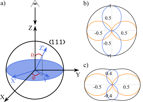
The transitions A and D can be described by a linear combination of the dipoles and (c.f. reference [14]). A rotation of the ND around the angle therefore leads to a change of the polarization contrast in the polarization plots of the transitions A and D (see figure 5(b),(c)). The polarization contrast of the A and D transitions can be calculated using equation (4):
| (5) |
For the angle we obtain
| (6) |
From our measurements we calculate a change of the polarization contrast from to for transition A and from to for transition D during the nanomanipulation, resulting in a rotation of the ND around the angle = .
ND fabrication
The details of the ND synthesis are described in the main text. We here show SEM images of the diamond nanoparticles that are in size (figure 6).
Evaluation of spectral diffusion in PLE scans
We study spectral diffusion of transition C of the SiV- center of figure 1(d) of the main paper. Therefore we plot the histogram of several PLE scans and fit the data with a Lorentzian function (figure 7(a)) and a Gaussian function (figure 7(b)). The Gaussian fit underestimates the peak maximum resulting in a broader linewidth compared to the Lorentzian fit. In the main paper we therefore extract the PLE linewidth of the SiV- center from the Lorentzian fit.
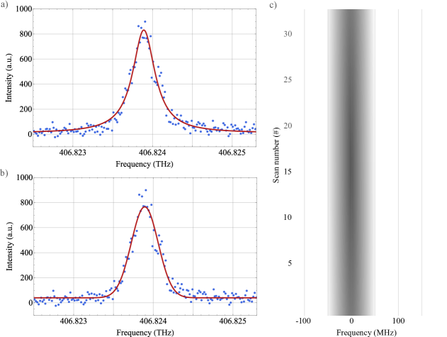
Spectral diffusion of the line becomes visible when investigating the peak position of single PLE scans (figure 7(c)). We observe spectral jumps of the resonance frequency on the order of the previously determined histogram linewidth of .