Perspective: Heusler interfaces – opportunities beyond spintronics?
Abstract
Heusler compounds, in both cubic and hexagonal polymorphs, exhibit a remarkable range of electronic, magnetic, elastic, and topological properties, rivaling that of the transition metal oxides. To date, research on these quantum materials has focused primarily on bulk magnetic and thermoelectric properties or on applications in spintronics. More broadly, however, Heuslers provide a platform for discovery and manipulation of emergent properties at well-defined crystalline interfaces. Here, motivated by advances in the epitaxial growth of layered Heusler heterostructures, I present a vision for Heusler interfaces, focusing on the frontiers and challenges that lie beyond spintronics. The ability to grow these materials epitaxially on technologically important semiconductor substrates, such as GaAs, Ge, and Si, provides a direct path for their integration with modern electronics. Further advances will require new methods to control the stoichiometry and defects to “electronic grade” quality, and to control the interface abruptness and ordering at the atomic scale.
The properties at materials interfaces often exceed the simple sum of their bulk constituents. Prime examples include the two-dimensional electron gas at the interface between insulators LaAlO3 and SrTiO3 Ohtomo and Hwang (2004); the order of magnitude enhancement of the superconducting critical temperature at the monolayer FeSe/SrTiO3 interface Qing-Yan et al. (2012); He et al. (2013); Lee et al. (2014a); topological states at the interfaces between topological materials and normal materials (or a surface) Hsieh et al. (2008); Chen et al. (2009); modulation doping in semiconductor heterostructures Dingle et al. (1978) for discoveries in fundamental physics (e.g. integer Klitzing et al. (1980); Tsukazaki et al. (2007) and fractional Tsui et al. (1982); Stormer et al. (1999) quantum Hall effects) and application in high electron mobility transistors (HEMTs Dingle et al. (1979); Asif Khan et al. (1993); Mimura (2002)), and the band bending, carrier confinement, and current rectification at semiconductor interfaces (e.g. GaAs/AlGaAs, Si/Ge) Dingle et al. (1978); Kroemer (1957), which form the backbone of the modern microelectronics industry. Today, Herb Kroemer’s insight that “the interface is the device” extends well beyond the originally envisioned semiconductor interfaces Kroemer (2001).
In searching for new interfacial materials platforms, it is desirable to not only identify parent materials with a wide range of new functionality, but also to integrate these materials epitaxially with technologically important substrates. Heusler compounds are promising in both regards. The ternary intermetallic Heusler compounds have long held promise for their bulk thermoelectric Mastronardi et al. (1999); Zeier et al. (2016) and magnetic properties Graf et al. (2011); Wollmann et al. (2017), especially half-metallic ferromagnetism at room temperature for applications in spintronics De Groot et al. (1983). But their functional properties extend well beyond these topics of early focus, and now include topological states (Chadov et al., 2010; Lin et al., 2010; Logan et al., 2016; Liu et al., 2016a; Manna et al., 2018), superconductivity with novel pairing Brydon et al. (2016); Kim et al. (2018); Wernick et al. (1983); Nakajima et al. (2015); Timm et al. (2017); Wang et al. (2018), (ferro, antiferro, and ferri)-magnetism Suzuki et al. (2016); Tobola et al. (1998); Sanvito et al. (2017), skyrmions Nayak et al. (2017); Meshcheriakova et al. (2014), superelasticity and shape memory effect (ferroeleasticity) Liu et al. (2003), and predicted ferroelectricity and hyperferroelectricity Garrity et al. (2014a); Bennett et al. (2012). Combining these functionalities at atomically defined interfaces presents opportunities to discover and manipulate emergent properties that do not exist in the bulk, e.g., via the application of epitaxial strain, quantum confinement, proximity effects, and band discontinuities. Furthermore, due to their close symmetry- and lattice-match to zincblende semiconductors, many Heuslers can be grown epitaxially on semiconductor substrates such as GaAs, GaSb, Si, and Ge, providing a template for their integration with modern electronics.
In this Perspective I offer a vision for Heusler interfaces as a platform for interfacial materials discovery and design. A number of excellent reviews on magnetic Heuslers and their applications in spintronics already exist, for which the reader is referred to Refs. Farshchi and Ramsteiner (2013); Felser et al. (2015); Hirohata et al. (2006); Wollmann et al. (2017); Palmstrøm (2016, 2003); Casper et al. (2012); Felser and Hirohata (2016); Graf et al. (2011). Here I look ahead to the opportunities and challenges that lie beyond spintronics, where the plethora of competing ground states Chadov et al. (2010); Lin et al. (2010); Manna et al. (2018), combined with advances in epitaxial film growth Bach et al. (2003a); Palmstrøm (2016); Kawasaki et al. (2014), theory Kawasaki et al. (2018); Sharan et al. (2019); Picozzi and Freeman (2007), and characterization Kawasaki et al. (2018); Logan et al. (2016); Liu et al. (2016a); Brown-Heft et al. (2018); Andrieu et al. (2016); Jourdan et al. (2014), position Heuslers as an intriguing platform for interfacial materials design. Further advances will require new methods to control the stoichiometry and defects in Heuslers to “electronic grade” quality, and to control interface abruptness and ordering at the atomic scale. I discuss the opportunities and challenges for Heusler interfaces, in both cubic and hexagonal polymorphs. The broad array of functionality in Heuslers is highly complementary to that of the transition metal oxides Mannhart and Schlom (2010), but from the opposite starting point: whereas oxides are generally brittle insulating ceramics that can be made conductive, Heuslers are ductile conductive intermetallics that can be made insulating.
Quantum materials, minus the oxygen
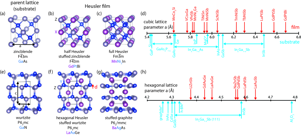
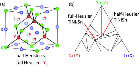
Heusler compounds are intermetallic compounds that crystallize in one of several stuffed tetrahedral structures. Conventionally the term “Heusler” has been reserved for the cubic polymorphs, but here I expand the term to include the hexagonal analogues (Fig. 1). The cubic half Heusler compounds (Fig. 1b, spacegroup , structure) have composition and consist of a zincblende sublattice that is “stuffed” with at the octahedrally coordinated sites Kandpal et al. (2006). Alternatively, this structure can be viewed as a rocksalt sublattice that is “stuffed” with in every other tetrahedral interstitial site Öğüt and Rabe (1995); Larson et al. (2000). Full Heusler compounds, with composition , contain an additional atom in the basis to fill all of the tetrahedral interstitials (Fig. 1c, structure) Graf et al. (2011). Here I adopt the naming convention of ordering the elements by increasing electronegativity, i.e. and (TiCoSb and MnNi2Ga ), rather than the often adopted and (CoTiSb and Ni2MnGa)Knowlton and Clifford (1912); Heusler (1903), for consistency with standard naming conventions of other compounds 111Multiple conventions have been used for naming cubic and hexagonal Heusler compounds. The naming of hexagonal Heuslers typically follows the convention of listing constituents in order of increasing electronegativity , e.g. LaCuSn and LiGaGe. The naming of cubic half Heusler compounds often follows this convention, e.g. LuPtBi, TiCoSb, and TiNiSn; however, the ordering is also commonly used, e.g. CoTiSb and NiTiSn. This alternate convention exists because full Heusler compounds are more commonly written (e.g., Ni2MnGa) rather than (MnNi2Ga). For consistency across the cubic and hexagonal Heusler compounds, this article adopts the electronegativity convention. When another notation is more commonly used, that name is also mentioned.. Lattice parameters for most cubic Heuslers are spanned by the zincblende III-V semiconductors, from GaP ( Å) to GaAs ( Å) and InSb ( Å). Relaxed ternary buffer layers, e.g., InxGa1-xAs, enable the lattice parameter to be tuned exactly (Fig. 1d).

Hexagonal polymorphs also exist, in which polar distortions give rise to properties that are not symmetry-allowed for cubic systems, e.g., ferroelectricity. The parent ZrBeSi-type structure is nonpolar and consists of planar graphite-like layers that are “stuffed” with (spacegroup Fig. 1g). Unidirectional buckling of the layers produces the polar LiGaGe-type structure, which can be viewed as a “stuffed wurtzite” (spacegroup , Fig. 1f) Casper et al. (2008); Hoffmann and Pöttgen (2001). Many insulating materials are promising as ferroelectrics, with calculated polarization and energy barrier to switching comparable to BaTiO3 Bennett et al. (2012); Garrity et al. (2014a), despite being composed of all-metallic constituents. These predictions challenge the conventional notion that good ferroelectrics should be highly ionic materials with large Born effective charges Benedek and Stengel (2014). In fact, it is precisely this lack of ionicity and stronger tendency towards covalent bonding that is predicted to make many hexagonal Heuslers robust against the depolarizing field, making them hyperferroelectrics Garrity et al. (2014a). Other polar materials are natively semimetallic, and are of interest as low resistivity polar metals Benedek and Birol (2016). These hexagonal materials are “stuffed” versions of wurtzite GaN (polar) and hexagonal BN (nonpolar), and can be lattice matched to zincblende semiconductor substrates in orientation (Fig. 1h).
In both hexagonal and cubic polymorphs, is typically a transition or rare earth metal, a transition metal, and a main group metal (III, IV, or V). The phase boundary between hexagonal and cubic polymorphs is determined by the relative size of the cation compared to and , with larger cations favoring the hexagonal polymorphs and smaller favoring cubic polymorphs Seibel et al. (2015); Hoffmann and Pöttgen (2001); Casper et al. (2008); Xie et al. (2014). This dependence on chemical pressure suggests that the phase boundary could also be traversed by epitaxial strain, giving the epitaxial grower access to phases that would otherwise be challenging to stabilize and retain by bulk synthetic methods, e.g., hydrostatic pressure. Other structural variants include Jahn-Teller driven cubic to tetragonal distortions, variations in the atomic site ordering (e.g. “inverse Heusler,” , and cubic variants), and polar vs antipolar layer buckling patterns in the hexagonal variants Seibel et al. (2015); Bennett et al. (2013); Strohbeen et al. (2019).
The wide array of quantum properties in these materials arises from the large orbital degeneracy and the spatial confinement of and orbitals (compared to and ), with rich phenomena that are highly complementary to that observed in the transition metal oxides. Due to their lack of oxygen or other highly electronegative species, Heusler compounds are typically less ionic than oxides and the on-site electron-electron repulsion (Coulomb ) is generally weaker. For these reasons, Heusler compounds are unlikely to be a good system for finding new high temperature superconductors Dagotto (1994). On the other hand, magnetic exchange interactions (Hund’s ) are quite significant, as evidenced by the strong tendency for magnetic ordering with Curie temperatures as large as 1100 K Wurmehl et al. (2006). The lack of oxygen combined with substrate lattice matching make Heuslers more amenable than oxides to integration with compound semiconductors, since oxygen interdiffusion, reactions, and misfit dislocations pose significant challenges for oxide on semiconductor epitaxy Hubbard and Schlom (1996). Additionally, many Heusler compounds can be alloyed via to form quaternary, quinary, and even higher component alloys, providing a means to continuously tune the lattice parameter and properties of the Heusler compound itself Zeier et al. (2016). Finally, whereas oxides are typically brittle, Heuslers are highly elastic, displaying superelasticity and accommodating strains of several percent without plastic deformation Bungaro et al. (2003); Dong et al. (2004), making them attractive for flexible magnetoelectronics.
Opportunities at interfaces
Many of the most intriguing properties arise when the diverse properties of Heuslers can be combined and manipulated at atomically defined interfaces (Fig. 2). Such interfaces include Heusler/semiconductor, Heusler/oxide, and interfaces between two different Heusler compounds. Here I highlight several opportunities that lie beyond spintronics, and in the next section I describe the key experimental challenges.
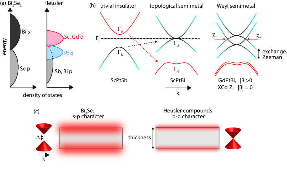
Topological states. Recent angle-resolved photoemission spectroscopy (ARPES) measurements Logan et al. (2016); Liu et al. (2016a) confirm theoretical predictions Lin et al. (2010); Chadov et al. (2010) of topological surface and interface states in cubic half Heuslers with large spin-orbit coupling compared to the bandwidth (), e.g. PtBi and PtSb ( rare earth metal) (Fig. 3b). Such states arise at the interfaces between topologically band-inverted materials and normal materials (or the vacuum, i.e. a surface), and are of great importance for dissipationless transport and for discovery of emergent quasiparticles when interfaced with layers of other functionality, e.g., Majorana bound states at topological / superconductor interfaces Fu and Kane (2008).
Compared to first-generation binary topological insulators BixSb1-x and Bi2Se3, Heuslers offer several distinct opportunities. Firstly, whereas in most known topological materials the near-Fermi level states have and character, Heuslers have significant transition metal character with moderate electron-electron correlations Chadov et al. (2009) (Fig. 3a). The interplay between correlations and spin-orbit coupling is predicted to yield rich correlated topological properties in other systems, e.g. axion states and topological Kondo insulators in iridates. Kim et al. (2008); Witczak-Krempa et al. (2014). Heuslers provide an alternative materials system for realizing such phenomena. Another potential consequence of localized orbitals is a shorter critical length scale for surface and interface state hybridization (Fig. 3c). ARPES measurements of ultrathin Bi2Se3 films reveal that below a critical thickness of six quintuple layers ( nm), the topological states at top and bottom interfaces hybridize to open a gap Zhang et al. (2010). The smaller spatial extent of states in Heuslers implies that topological states may survive to smaller critical thicknesses without gapping out.
Secondly, the multifunctionality within the Heusler family enables lattice-matched topological heterostructures, for interfacing topological states with layers of other functionality. For example, topological / superconductor interfaces are predicted to host Majorana bound states, and topological / ferromagnet interfaces are expected to exhibit the quantum anomalous Hall effect Chang et al. (2013); Liu et al. (2016b) and axion states Xiao et al. (2018); Mogi et al. (2017). Lattice matching minimizes the potentially detrimental effects of misfit dislocations and interfacial defect states that could otherwise obscure the property of interest Richardella et al. (2015), e.g., by acting as parasitic conduction channels.
Finally, Heuslers are a platform for other topological states, including Dirac and Weyl fermions, in both cubic and hexagonal polymorphs. In cubic Heuslers, transport signatures of Weyl nodes have been observed in several PtBi compounds Hirschberger et al. (2016); Liang et al. (2018); Shekhar et al. (2018); Singha et al. (2019) and MnCo2Ga (also known as Co2MnGa) Sakai et al. (2018) under an applied magnetic field, and theory predicts Weyl nodes in the magnetic full Heuslers Co without an external field Wang et al. (2016) (Fig. 3b). In the hexagonal polymorphs, which break inversion symmetry, DFT calculations predict Weyl nodes Narayan (2015); Gao et al. (2018) whose momenta are highly sensitive to the magnitude of polar buckling, potentially tunable by epitaxial strain.
Interfacial superconductivity. Heuslers are a platform for novel superconductivity, both at artificially defined interfaces and natively due to strong spin-orbit coupling. Whereas most known superconductors have singlet pairing, triplet superconductivity is predicted at interfaces between conventional superconductors and ferromagnets Bergeret et al. (2001). Signatures of triplet pairing have been observed experimentally in Heusler-based Josephson junctions, where Nb and MnCu2Al Sprungmann et al. (2010). All-Heusler Josephson junctions offer the potential of realizing such behavior in fully-lattice matched systems that minimize interfacial disorder. Examples of Heusler superconductors include the cubic full Heuslers Pd2Sn (Sc, Y, Lu) and Pd [ (Zr, Hf), (In, Al)] (also known as Pd) Klimczuk et al. (2012); Winterlik et al. (2009); the rare earth containing half Heuslers PdBi Nakajima et al. (2015); Kim et al. (2018); and the hexagonal compounds BaPtAs Kudo et al. (2018), SrPtAs Nishikubo et al. (2011), and YbGaSi Imai et al. (2008). Heusler Josephson junctions are also a platform phase control in an all epitaxial system, with potential applications as qubits Yamashita et al. (2005).
Intriguingly, recent theory Brydon et al. (2016); Venderbos et al. (2018) and experiments Kim et al. (2018) suggest triplet and higher order pairing may exist natively in a subset of topological superconducting half Heuslers with composition PdBi. Here the pairing occurs between fermions due to strong spin-orbit coupling. This combination is expected to natively host Majorana states in a single material Yang et al. (2017), in contrast with previous experimental realizations that rely on an interface between a superconductor and a separate high spin-orbit material Mourik et al. (2012).
Interface polarization: ferroelectrics and polar metals. For conventional ferroelectrics, the depolarizing field typically competes with and destroys long range polar order in the limit of ultrathin films. Hexagonal Heusler interfaces offer two potential solutions to this problem. Firstly, a number of insulating compounds (e.g., LiZnAs, NaZnSb) have been proposed as hyperferroelectrics, which are robust against the depolarizing field due to their highly covalent bonding character with small Born effective charges Garrity et al. (2014a). Ferroelectric switching and hyperferroelectricity have yet to be experimentally demonstrated in hexagonal Heuslers. A significant challenge is that only a small subset of hexagonal Heuslers is natively insulating - an assumed requirement for switching via applied electric fields Fei et al. (2018). Epitaxial strain, quantum confinement, and Peierls-like distortions Seibel et al. (2015); Strohbeen et al. (2019); Genser et al. (2019) may provide routes for tuning the buckling and opening a gap in polar compounds that are natively metallic.
For those hexagonal compounds that cannot be made insulating, the coexistence of a polar structure and metallicity holds interest in its own right, and may be a second solution to the depolarizing field problem. Polar metals, once assumed to be unstable since free carriers were thought to screen out polar displacements, are not fundamentally forbidden Anderson and Blount (1965) and have recently been demonstrated in several transition metal oxides Shi et al. (2013); Cao et al. (2018); Kim et al. (2016, 2016). Hexagonal Heuslers are another family of polar metals, and are unique in that they are generally more conductive than oxides Kaczorowski et al. (1999); Schnelle et al. (1997). One application for polar metals may be to suppress the effects of the depolarizing field by pinning displacements at the polar metal / ferroelectric interface Puggioni et al. (2016). Other opportunities for polar metal interfaces may lie in nonlinear optics Wu et al. (2017), nonlinear charge transport Kang et al. (2019); Tokura and Nagaosa (2018), and novel superconductivity Edelstein (1995).
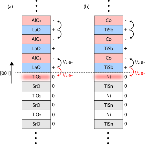
Polar catastrophe. Interface polarization and charge transfer also provide opportunities for the creation of two-dimensional electron gasses (2DEGs) across interfaces. Consider the classic “polar catastrophe” 2DEG that emerges at the LaAlO3 / SrTiO3 interface (Fig. 4a). In this electron system, the (001) stacking sequence of SrTiO3 consists of charge neutral SrO/TiO2 atomic planes, while LaAlO3 consists of LaO/AlO2 atomic planes with alternating charge Ohtomo and Hwang (2004); Janotti et al. (2012). The 2DEG arises from charge transfer of half an electron per formula unit across the interface, from the LaO atomic plane in LaAlO3 to the TiO2 atomic plane in SrTiO3 Ohtomo and Hwang (2004); Janotti et al. (2012). The half Heusler system TiNiSn / TiCoSb contains the same essential ingredients: just like LAO/STO, the near Fermi level orbitals also have strong character. In (001) orientation the Ni/TiSn atomic planes are formally charge neutral, while the Co/TiSb planes have formal charges Kawasaki et al. (2018) (Fig. 4b). These formal charges are based on an electron counting model Kawasaki et al. (2018) that accurately predicts the experimentally measured surface reconstructions of TiCoSb (001), and is consistent with the experimental data for LuPtSb Patel et al. (2014, 2016), MnNiSb Bach et al. (2003a), and TiNiSn (001) Kawasaki et al. (2013).
In this highly simplified view, a charge transfer 2DEG might also be expected at this Heusler interface Sharan et al. (2019). Recent transport measurements on MBE-grown TiCoSb/TiNiSn bilayers show 1.5 order of magnitude enhanced conductivity Rice (2017), consistent with this interfacial charge transfer prediction Sharan et al. (2019). Additionally, in LaAlO3 / SrTiO3 the strong spatial confinement of the 2DEG has been suggested to enhance electron-electron correlations and contribute to the emergent superconductivity. What new properties may emerge at Heusler interfaces with enhanced correlations?
Interfacial magnetism and skyrmions. Heusler interfaces offer a platform for enhancing skyrmion phase stability via combined bulk and interfacial inversion symmetry breaking. Magnetic skyrmions are topologically protected vortex-like swirls of spin texture, whose robustness against atomic scale disorder makes them attractive for applications in magnetic memory. They are stabilized Roessler et al. (2006); Binz and Vishwanath (2006); Han et al. (2010) by the Dzyaloshinskii-Moriya (DM) exchange interaction Dzyaloshinsky (1958); Moriya (1960), which results from a combination of broken inversion symmetry and large spin-orbit coupling. To date, most work has focused on two separate strategies to stabilize skyrmions: (1) bulk crystal structures that break inversion, e.g. crystals such as FeGe and MnSi Mühlbauer et al. (2009), or (2) artificially defined interfaces that break inversion Bogdanov and Rößler (2001), e.g. Co/Pt interfaces Yang et al. (2015).
Combining bulk and interfacial DM interactions in a single materials platform is predicted to be a path towards further control and enhancements of skyrmion stability Rowland et al. (2016). Heuslers are a strong materials candidate. Recent experiments confirm skyrmions in several Mn compounds that crystallize in the tetragonal inverse Heusler structure () that breaks bulk inversion Nayak et al. (2017); Meshcheriakova et al. (2014). The epitaxial film growth of several of these compounds has recently been demonstrated Jin et al. (2018); Swekis et al. (2019); Rana et al. (2016); Meshcheriakova et al. (2015); Li et al. (2018) providing a path towards further manipulation of the DM interaction in layered heterostuctures of these materials. Beyond skyrmion stability, recent theoretical proposals suggest that skyrmion/superconductor interfaces may be another platform for hosting Majorana fermions Yang et al. (2016); Chen and Schnyder (2015), potentially realizable in an all-Heusler system.
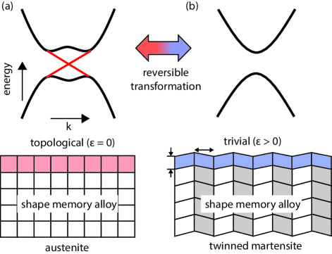
Interface strain and shape memory effect. Shape memory alloys are ferroelastic materials that undergo large, reversible martensitic phase transitions or twin reorientations to revert a macroscopically deformed material back to its original shape. Several Heuslers, including MnNi ( group III or IV) and MnCo2Ga, exhibit such transitions, driven by temperature and strain (shape memory effect), or by an external magnetic field (magnetic shape memory effect) Dong et al. (2004); Bungaro et al. (2003). These compounds are also known as Ni2Mn and Co2MnGa. Across these transitions the magnetic, caloric, and electrical transport properties change abruptly Mañosa et al. (2010), and these materials are generally also superelastic, accommodating strains as large as 10 percent by locally undergoing strain-induced martensitic phase transitions or twin reorientations Sozinov et al. (2002). This 10 percent strain is an order of magnitude larger than the strains observed in magnetostrictive or piezoelectric materials, with promising applications for microactuation and vibration dampening. The large latent heat associated with the phase transition holds promise for applications in refrigeration and thermal energy conversion Srivastava et al. (2011); Song et al. (2013).
Layered heterostructures composed of a shape memory alloy provide an opportunity to couple the large and reversible strains across materials interfaces, to induce phase transitions in adjacent functional layers. For example, DFT calculations suggest that the topological band inversion in the PtBi Heuslers can be flipped by strains of approximately 3% Chadov et al. (2010). One could envision PtBi / shape memory alloy interfaces in which the topological states are switched “on” and “off” by temperature or magnetic field-induced martensitic phase transitions (Fig. 5). Strains of this magnitude are likely too large to be produced by coupling to magnetostrictive or piezoelectric layers, but are within the limits of shape memory alloys.
Well-defined epitaxial interfaces also provide an idealized test bed for understanding and manipulating the phase transition itself. A key limiting factor in bulk shape memory alloys is that the habit plane, i.e. the interface between austenite and martensite phases, is not guaranteed to be atomically commensurate (epitaxial). As a result, repeated cycling through the martensitic phase transition creates dislocations that lead to slower switching speeds, decreased energy efficiency, and eventually mechanical failure Gall and Maier (2002). A promising materials design route is to engineer materials such that the habit plane is atomically commensurate or near-commensurate, i.e. the compatibility and cofactor conditions James and Hane (2000); James and Kinderlehrer (1989); Bhattacharya (1991); Ball and James (1987); Gu et al. (2018). This condition is met when the middle eigenvalue of the austenite to martensite transformation matrix equals 1. One design route towards the criterion is to deliberately fabricate non-stoichiometric samples Cui et al. (2006); Chluba et al. (2015), such as Mn25+yNi50-xCoxSn25-y (also known as Ni50-xCoxMn25+ySn25-y) Srivastava et al. (2010); Bhatti et al. (2012).
Another route is to engineer the habit plane via film/substrate interface effects in epitaxial thin films, which can be tuned via crystallographic orientation and strain Bhattacharya et al. (1999); Kaufmann et al. (2011). For example, for epitaxial NiTi films grown on (001) oriented MgO Buschbeck et al. (2011a) and GaAs Buschbeck et al. (2011b) substrates, clamping effects from the substrate force a new transformation pathway in which the habit plane lies parallel to the (001) Buschbeck et al. (2011a). Importantly, this transformation occurs via a shear mechanism in which the interface remains atomically coherent, and may provide a general route towards engineering atomically commensurate phase transitions.
Challenges
Significant advances have been made on the epitaxial growth and control of Heusler interfaces over the past 20 years, primarily driven by applications in spintronics. These include the development of Heusler molecular beam epitaxy (MBE) Ambrose et al. (2000); Van Roy et al. (2000); Bach et al. (2003a); Dong et al. (1999, 2000); Turban et al. (2002), the identification of semi adsorption-controlled growth windows Kawasaki et al. (2018); Patel et al. (2014); Bach et al. (2003b); Turban et al. (2002); Strohbeen et al. (2019), the use of epitaxial diffusion barriers and low temperature seed layers Palmstrøm (2016); Farshchi and Ramsteiner (2013); Schultz et al. (2002); Buschbeck et al. (2011b), the use of chemical templating layers Dong et al. (2000); Filippou et al. (2018), and the development simple theoretical frameworks based on electron counting Kandpal et al. (2006); Jung et al. (2000); Pashley (1989) for predicting stability and structural distortions at surfaces and interfaces Kawasaki et al. (2018); Pashley (1989).
Despite these advances, the full realization of Heusler properties beyond spintronics will likely require even more stingent control of materials and interface quality. This is because many of the emerging properties in Heuslers depend on bandgaps: bulk bandgaps in topological insulators and ferroelectrics, minority spin gaps in half metals, and pairing gaps in superconductors. Such gaps tend to be highly sensitive to non-stoichiometry, point defects, lattice distortions, and interfacial reconstructions and disorder. Additionally, interfacial properties are often inherently short-range, and therefore can be sensitive subtle changes in atomic structure across the interface.
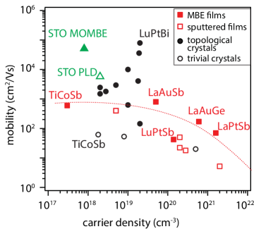
Controlling stoichiometry and defects to “electronic grade.” Although bandstructure calculations predict a number of half Heuslers to be semiconductors with bandgaps of 1 eV or larger, typical background carrier densities are well above cm-3 and mobilities below cm2/Vs, for both bulk crystals and thin films (Fig. 6). Flux-grown single crystals of Heusler topological semimetals do have higher mobilities approaching cm2/Vs (filled black circles Hou et al. (2015a); Hirschberger et al. (2016); Hou et al. (2015b); Nakajima et al. (2015)); however, this higher mobility results in part from the topological protection of surface or bulk Dirac and Weyl states rather than purely a reduction of bulk impurity scattering.
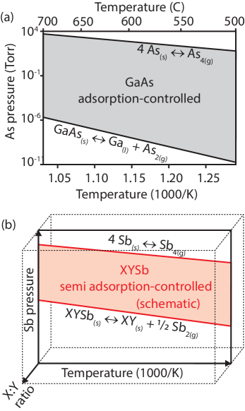
The poor transport properties stem largely from challenges in controlling the stoichiometry and resultant defects, which are generally more difficult to control in ternary intermetallics than in simple binary semiconductors. To illustrate this challenge, consider binary GaAs, which shows record high electron mobility when grown in a modulation doped structure by MBE Dingle et al. (1978); Pfeiffer and West (2003); Gardner et al. (2016). A major reason for the success of MBE-grown GaAs is the existence of a thermodynamically adsorption-controlled growth window Tsao (2012), in which the stoichiometry is self-limiting (Fig. 7(a)). Due to the high volatility of arsenic, GaAs films are grown with an excess arsenic flux, in which only the stoichiometric As:Ga ratio “sticks” and the excess arsenic escapes in the vapor phase. High mobility ternary III-V alloys, e.g. InxGa1-xAs, are also routinely grown by MBE in which the As:(In+Ga) stoichiometry is self-limiting. The In:Ga stoichiometry is not self-limiting; however, since both In and Ga have the same valence and incorporate substitutionally on the same lattice sites, slight variations of In:Ga composition result in subtle changes in the bandgap rather than the formation of defect states.
In select cases, ternary Heuslers can be grown in a semi adsorption-controlled window (Fig. 7b), in which the stoichiometry of one of the three elements is self-limiting. TiCoSb Kawasaki et al. (2018, 2014), MnNiSb Bach et al. (2003b); Turban et al. (2002), LuPtSb Patel et al. (2014), and LaAuSb Strohbeen et al. (2019) can be grown by MBE with an excess Sb flux, in which the ratio of Sb to is self-limiting.The TiCoSb films grown by this method display the lowest background carrier concentration ( cm-3, cm-3) of any gapped Heusler compound to date Kawasaki et al. (2014), including bulk crystals (Fig. 6). The electron mobility of cm2/Vs is similarly large, compared to typical values of less 100 cm2/Vs for growth by sputtering or arc melting (Fig. 6). For the semimetal LaAuSb grown by semi adsorption-controlled MBE, the 2K mobility is 800 cm2/Vs Strohbeen et al. (2019).
However, it remains an outstanding challenge to control the remaining transition metal stoichiometry. This is especially important for Heuslers, compared to III-V ternary alloys, since and occupy different lattice sites and typically have different valences. At typical growth temperatures of C the sticking coefficients for elemental transition metals are near unity, therefore the film stoichiometry relies on precise control of and fluxes rather than a self-limiting process. Due to typical flux drifts, these fluxes are difficult to control to better than , even when using real-time flux monitoring and feedback approaches such as optical atomic absorption Chalmers and Killeen (1993); Kasai and Sakai (1997)) or x-ray emission (RHEED-TRAXS Hasegawa et al. (1985)) spectroscopies. In a worst-case scenario, if all nonstoichiometric defects were electrically active, a deviation in stoichiometry would correspond to an unintentional carrier density of order cm-3, clearly unacceptable for most electronic applications. At such high concentrations, the defects typical form an impurity band or a “perturbed host” band Yonggang et al. (2017). While not all defects are electronically active Yonggang et al. (2017), experimentally it is found that most polycrystalline half Heuslers have carrier densities greater than cm-3 Muta et al. (2009); Kim et al. (2007); Fu et al. (2015). In general only flux-grown single crystals and semi adsorption-controlled MBE films have unintentional densities below cm-3 (Fig. 6). Control of stoichiometry is also critical for half-metallic ferromagnets, since non-stoichiometric defects often produce states within the minority spin gap Picozzi and Freeman (2007), thus decreasing the spin polarization at the Fermi energy.
One possible solution may to replace one or both of the transition metal sources with a volatile chemical precursor. For transition metal oxides, fully adsorption-controlled growth of SrTiO3 and SrVO3 thin films has been demonstrated by replacing elemental Ti and V with titanium tetra-isopropoxide (TTIP) and vanadium tetra-isopropoxide (VTIP), respectively. The resulting films exhibit record high electron mobility Cain et al. (2013); Son et al. (2010) and low residual resistivity Moyer et al. (2013), exceeding their bulk counterparts. This approach is generally called metalorganic molecular beam epitaxy (MOMBE) Pütz et al. (1985) or chemical beam epitaxy (CBE) Tsang (1984). First developed in the 1980’s for growth of III-Vs, MOMBE was applied a few years later to the growth of superconducting oxides Ba2Cu3O7-x ( Y, Dy) King et al. (1991); Endo et al. (1991). For the case of perovskite oxides, this approach has recently been termed hybrid MBE (hMBE) Jalan et al. (2009a, b), where the distinction hybrid refers to the combined use of metalorganicelementalgas sources Brahlek et al. (2018), as opposed to purely metalorganic or metalorganicelemental sources. Given the remarkable success of volatile precursor MBE for transition metal oxide growth, similar advances are anticipated if the approach can be applied to Heuslers. Potential precursors include metalorganics, e.g. the metal cyclopentadienyls, or volatile metal halides. However, such precursors introduce new challenges of potential carbon incorporation and equipment corrosion, respectively.
Ultimately, the degree of stoichiometry control possible by adsorption-control may be limited by the phase diagram of the particular system. For example, rather than existing as pure line compounds, some Heusler compounds have a finite (few percent) phase field along certain directions in composition space. The solubility of excess Ni within TiNi1+xSn is one example Douglas et al. (2014a); Rice et al. (2017); Douglas et al. (2014b). For such compounds, the stoichiometry is likely to only be self-limited to within the bounds of the phase field. However, for certain applications deliberately off-stoichiometric compositions are desired, e.g. the criterion for low hysteresis shape memory alloys as described in the previous section James and Hane (2000); James and Kinderlehrer (1989); Bhattacharya (1991); Ball and James (1987); Gu et al. (2018).
Point defects. Point defects in Heuslers also remain challenging to understand, measure, and control, in part because a quantitative experimental identification requires relatively low defect density samples. Our understanding is derived primarily from first-principles theory. DFT calculations on cubic full and half Heuslers predict a number of point defects, many with similarly small formation energies ( eV) Yonggang et al. (2017); Picozzi and Freeman (2007); Picozzi et al. (2004). The hexagonal polymorphs are less explored.
For half Heuslers, DFT calculations suggest the defect behavior may be grouped into families based on the chemical identity of the site Yonggang et al. (2017). For metal, interstitials ( on interstitial sites, Fig. 8a) are predicted to be the dominant low energy defect Yonggang et al. (2017), consistent with previous specific calculations for Ni Larson et al. (2000); Öğüt and Rabe (1995). These findings are consistent with the structural insight that and sites have the same nearest neighbor coordination, and therefore filling these sites would have similar energies ( to eV, depending on the position of the chemical potential Yonggang et al. (2017)). In the dilute limit, interstitials are expected to act as shallow donors Yonggang et al. (2017). In the high concentration limit they are expected to decrease the effective bandgap via the formation of an impurity band or a “perturbed host” band, which explains why many of the predicted semiconducting Heuslers behave experimentally as metals in transport measurements. The low formation energy for is also proposed to drive a natural tendency for half Heuslers to be -rich Yonggang et al. (2017). This prediction of natural off stoichiometry is consistent with experimental observations that for TiNiSn, the phase field extends towards excess Ni and a thermodynamic tie line exists between half Heusler TiNiSn and full Heusler TiNi2Sn (Fig. 8b) Douglas et al. (2014a); Rice et al. (2017); Douglas et al. (2014b). Such a tie line exists in many other half Heusler / full Heusler systems, e.g. ZrNiSn / ZrNi2Sn and TiCoSn / TiCo2Sn. Additionally, the electrical transport for TiNi1+xSn is optimized (low carrier density, high mobility) for samples that are slightly Ni rich (), suggesting that the excess Nii compensates electrically for the natural Ni vacancy () formation Rice et al. (2017). A fruitful new direction for theorists would be to identify other electrically compensating point defects, to guide experimental efforts in making half Heuslers that are truly insulating.
For half Heuslers, antisites are expected to be the dominant defect, which act as acceptors Yonggang et al. (2017). General trends for are not well established Yonggang et al. (2017).
Similar defect calculations for full Heuslers suggest vacancies () to be a low energy defect Popescu et al. (2017), complementary to the for half Heuslers. This prediction is consistent with experimental observations that full Heusler TiNi2-xSn has a finite phase field extending in the Ni-deficient direction Romaka et al. (2013). and antisites are another proposed defect in both full and half Heuslers Larson et al. (2000); Popescu et al. (2017), consistent with experimental observations of -type disorder Khovailo et al. (2001), in which and sites are indistinguishable, for films grown at low temperature Rath et al. (2018). and antisites have also been proposed: in MnCo2Si, first-principles calculations suggest MnCo (Mn on Co lattice sites) have lowest formation energy and generally retain half metallic character, but other defects such as CoMn are close in formation energy and can destroy half metallicity by forming states within the minority spin gap Picozzi et al. (2004). Given the large zoology of proposed point defects for full Heuslers, many with similar small calculated formation energies ( eV Picozzi et al. (2004); Picozzi and Freeman (2007); Yonggang et al. (2017), compared to eV for self interstitials in Si Rinke et al. (2009)), feedback between theory and measurements on clean samples are required to determine which defects are present, which are electronically active, and how to control them.
Interdiffusion and reconstructions. Most theoretical predictions assume idealized interfaces in which atoms adopt their bulk-like positions. However, at real materials interfaces there can be strong thermodynamic driving forces to deviate from simple bulk-like termination. This is especially important because interface properties are often inherently short-range. Heusler interfaces – including Heusler/Heusler, Heusler/III-V, and Heusler/oxide – are no exception. For Heuslers, the challenges exist at several length scales: interdiffusion and reactions at the several nanometer scale, and interfacial reconstructions and site disorder at the unit cell scale.
Interdiffusion and interfacial reactions pose significant challenges at some Heusler/III-V semiconductor interfaces, particularly those containing Ni or Mn. This stems from the large diffusion coefficients for many transition metals in III-Vs ( cm2/s for Mn and Ni in GaAs at 500 ∘C, compared to for typical main group species Wu et al. (1991); Lahav et al. (1986); Ruckman et al. (1986); Fisher (1998)), combined with complicated multi-component phase diagrams. These factors can result in interdiffused regions and secondary phases for direct Heusler on III-V growth at elevated temperatures (C Gusenbauer et al. (2011)). Interdiffusion also limits the sharpness of Heusler/Heusler interfaces (e.g. MnCo2Al / MnFe2Al Brown-Heft et al. (2018), TiNiSn / Zr0.5Hf0.5NiSn Jaeger et al. (2014), MnNiSb / MnPtSb Mancoff et al. (1999)), but is generally less significant at Heusler/oxide interfaces due to the relative stability of many metal-oxides (FeCo2Al / MgO Bai et al. (2014)).

One solution is to grow epitaxial diffusion barriers between the Heusler film and III-V substrate (Fig. 9a). The rare earth monopnictides (, rare earth, As, Sb, Bi) are highly effective diffusion barriers for group III and transition metal species Schultz et al. (2002); Palmstrom and Sands (1993). These materials have cubic rocksalt () structure and can can be lattice matched by alloying on the rare earth site. Examples include ErAs, ScxEr1-xAs, ErSb, and GdSb, which have enabled the epitaxial growth of a variety of intermetallic films on III-Vs at temperatures up to C Schultz et al. (2002); Buschbeck et al. (2011b); Palmstrøm (2016); Palmstrom and Sands (1993). However, the rare earth monopnictides are generally metallic, magnetic, and require a finite thickness of at least three atomic layers to be effective diffusion barriers. Hence they are not suitable when a direct Heusler/III-V interface is required.
Another approach is to grow thermodynamically stable, chemical templating layers Palmstrom and Sands (1993); Filippou et al. (2018) (Fig. 9b). interlayers (cesium chloride structure) are good templates for full Heusler growth, since these two structures are ordered variants of one another. Starting from the cubic structure, whose basis consists of at the origin and at the body center, the full Heusler structure is obtained by replacing every other site with . One example is to use a NiGa interlayer to seed the growth of MnNi2Ga on GaAs (001). NiGa is thermodynamically stable in contact with GaAs Dong et al. (2000), thus minimizing the interdiffusion. templating can also enhance the -axis ordering in Heuslers Filippou et al. (2018), since the [001] stacking sequence of a crystal with composition consists of alternating atomic planes of and . This template enhances the axis ordering of the subsequent Heusler film, due to the local bonding preference of on and on . However, like the rocksalt diffusion barriers, template layers are often metallic and require a finite thickness, and are also not suitable when a direct Heusler/III-V interface is required.
For direct Heusler/III-V interfaces or for interfaces between two different Heusler compounds, low temperature seed layers are the method of choice Palmstrøm (2016); Farshchi and Ramsteiner (2013) (Fig. 9c). This strategy consists of nucleating several unit cells of Heusler film at low temperature (C) to minimize interdiffusion during the formation of the interface Hashimoto et al. (2007); Kawasaki et al. (2014). The seed can be then be annealed and growth resumed at higher temperatures (C) to improve the degree of ordering Kawasaki et al. (2014); Hirohata et al. (2005); Hashimoto et al. (2007); Farshchi and Ramsteiner (2013); Palmstrøm (2016). This strategy relies on the fact that bulk diffusion is generally much slower than surface diffusion during growth. Once the interface is formed at low temperature, interdiffusion is suppressed for subsequent anneals compared to direct growth at higher temperatures, as inferred by reflection high energy electron diffraction and x-ray diffraction Hirohata et al. (2005); Kawasaki et al. (2014) or by device performance metrics such as the resistance-area product of a magnetoresistance junction Kubota et al. (2017). Direct measurements of the interdiffusion, e.g. by Rutherford Backscattering Spectrometry or STEM-EELS, are needed to fully quantify these effects as a function of post-growth anneal temperature.
For Heusler/III-V Rath et al. (2018); Nedelkoski et al. (2016) and Heusler/Heusler Brown-Heft et al. (2018) interfaces formed by low temperature seeds, the chemical intermixing is typically limited to a few atomic layers (Fig. 9d) Rath et al. (2018). However, due to the low surface diffusion at low temperatures, the seed layers often crystallizes in the disordered structure, in which and sites are indistinguishable, rather than the ordered full Heusler Farshchi and Ramsteiner (2013); Rath et al. (2018). The effects of such disorder on properties can vary significantly depending on the particular compound and desired property Orgassa et al. (2000); Farshchi and Ramsteiner (2013); Palmstrøm (2016); Wang et al. (2005); Inomata et al. (2008). Low temperature growth also impedes the ability to control stoichiometry and point defects, which are better controlled under high temperature, adsorption-controlled growth regimes Kawasaki et al. (2018); Patel et al. (2014); Bach et al. (2003b); Turban et al. (2002); Strohbeen et al. (2019).
Even for highly controlled chemical abruptness, thermodynamic driving forces can cause interfacial layer relaxations, atomic reconstructions, and even layer rearrangements. An extreme example is the MnCo2Si / GaAs (001) interface. The bulk (001) atomic stacking sequence of MnCo2Si (also known as Co2MnSi) consists of alternating atomic layers of MnSi and CoCo; however, photoemission spectroscopy measurements reveal that this interface tends to be Mn and As-rich, independent of whether the MnCo2Si growth on As-terminated GaAs is initiated with a monolayer of MnSi or CoCo Palmstrøm (2016); Patel (2015). Such atomic layer rearrangements are not unique to Heuslers, for example, they are also observed in layered perovskite oxides Nie et al. (2014); Lee et al. (2014b).
The strong thermodynamic driving forces place constraints on what interfaces can be synthesized, which is an important consideration since interface electronic states, half metallicity, charge transfer, and other interfacial properties can be highly sensitive to the interface termination Picozzi and Freeman (2007). Feedback from theory is crucial for identifying which types of interfaces are both stable and host the desired property Curtarolo et al. (2003); Sun et al. (2016); Curtarolo et al. (2005); Zunger et al. (2018). A significant challenge is that interfaces have reduced symmetry and increased atomic degrees of freedom, compared to the bulk. Given this potential complexity, it often is not practical to perform first-principles calculations for all possible interface atomic structures. There are too many candidate structures, and the large size of reconstructed slabs makes first-principles approaches computationally expensive. Simple models based on electron counting have recently been developed to guide the screening of stable structures at surfaces Kawasaki et al. (2018), which can be down selected for more accurate first-principles calculations. I anticipate that their generalization may make the interface problem more tractable.
Outlook
Heusler compounds are a remarkable family of interfacial materials, whose broad range of tunable properties is highly complementary to that of the well-studied transition metal oxides. These compounds are lattice-matched to technologically important semiconductor substrates, making them poised for impact in spintronics and beyond. I conclude with a few remarks on the role of theory and experiments going forward.
Theory. To date, theory has done an excellent job at screening for target properties in the bulk Oliynyk et al. (2016); Carrete et al. (2014); Garrity et al. (2014b); Bennett et al. (2012); Garrity et al. (2014a); Roy et al. (2012); Anand et al. (2019); Carrete et al. (2014); Sanvito et al. (2017) and predicting emergent properties at idealized interfaces, both at the level of first-principles DFT calculations Chadov et al. (2010); Lin et al. (2010); Picozzi and Freeman (2007); Picozzi et al. (2004); Zhu et al. (2015); Narayan (2015) and model Hamiltonians Timm et al. (2017); Brydon et al. (2016); Venderbos et al. (2018). Can such predictions be modified to account for more realistic structural distortions at Heusler interfaces, including relaxations, reconstructions, and point defects? Additionally, can theory aid in identifying which of these compounds and interfaces are thermodynamically stable, or more relevantly, “stabilizable?” New theoretical approaches are beginning to consider the path-dependent “remnant” metastability of bulk compounds Sun et al. (2016), to identify which compounds have local minima in the free energy landscape that lie not too far above the convex hull Aykol et al. (2018); Curtarolo et al. (2003, 2005); Zunger et al. (2018), and guide possible synthesis routes Sun et al. (2016); Chen et al. (2018). To what extent can these concepts be applied to Heuslers, and in particular, Heusler interfaces?
Experiments. Heusler compounds today are comparable to semiconductors in the early 20th century. Although field effect transistors were first proposed in the 1920’s and 30’s Edgar (28 January 1930, 7 March 1933); Heil (6 December 1935), the first experimental demonstrations of point contact transistors Bardeen and Brattain (1948) and field effect transistors Arns (1998); Kahng (27 August 1963) were not made until the late 40’s and 50’s. These discoveries were made possible by two major materials and interface innovations: (1) zone refining of germanium and silicon to reduce the background impurities, and (2) methods to prepare clean semiconductor / oxide interfaces, free of trapped charges.
Heusler compounds today are at a similar stage of development: a number of exotic phenomena have been predicted, but their full realization will likely require new advances in materials synthesis and interface control. In this Perspective I outlined a few of the key synthetic challenges and potential solutions. I look forward to the development of new feedback control methods during growth, new chemical precursors for self-limiting stoichiometry, and new methods to probe the properties of buried interfaces. Beyond the significant advances in Heusler spintronics, the broader field of Heusler interfaces is at a stage of relative infancy. I anticipate that the most exotic and the impactful properties of Heusler interfaces have yet to be unleashed.
I Acknowledgments
I thank Chris J. Palmstrøm for insightful feedback throughout the preparation of this manuscript and for his mentorship. I also thank Darrell G. Schlom and Jochen Mannhart Mannhart and Schlom (2010) for inspiring the title. I thank Richard D. James, Anderson Janotti, Chang-Beom Eom, Darrell G. Schlom, and Paul M. Voyles for their feedback, fruitful discussions, and collaborations.
This work was primarily supported by the CAREER program of the National Science Foundation (NSF DMR-1752797) and by the Young Investigator Program of the Army Research Office (ARO W911NF-17-1-0254). Additional support came from the NSF via the University of Wisconsin Materials Research Science and Engineering Center (MRSEC, DMR-1720415) and the Wisconsin Alumni Research Foundation (WARF).
References
- Ohtomo and Hwang (2004) A. Ohtomo and H. Hwang, Nature 427, 423 (2004).
- Qing-Yan et al. (2012) W. Qing-Yan, L. Zhi, Z. Wen-Hao, Z. Zuo-Cheng, Z. Jin-Song, L. Wei, D. Hao, O. Yun-Bo, D. Peng, C. Kai, et al., Chinese Physics Letters 29, 037402 (2012).
- He et al. (2013) S. He, J. He, W. Zhang, L. Zhao, D. Liu, X. Liu, D. Mou, Y.-B. Ou, Q.-Y. Wang, Z. Li, et al., Nature materials 12, 605 (2013).
- Lee et al. (2014a) J. Lee, F. Schmitt, R. Moore, S. Johnston, Y.-T. Cui, W. Li, M. Yi, Z. Liu, M. Hashimoto, Y. Zhang, et al., Nature 515, 245 (2014a).
- Hsieh et al. (2008) D. Hsieh, D. Qian, L. Wray, Y. Xia, Y. S. Hor, R. J. Cava, and M. Z. Hasan, Nature 452, 970 (2008).
- Chen et al. (2009) Y. Chen, J. G. Analytis, J.-H. Chu, Z. Liu, S.-K. Mo, X.-L. Qi, H. Zhang, D. Lu, X. Dai, Z. Fang, et al., science 325, 178 (2009).
- Dingle et al. (1978) R. Dingle, H. Störmer, A. Gossard, and W. Wiegmann, Applied Physics Letters 33, 665 (1978).
- Klitzing et al. (1980) K. v. Klitzing, G. Dorda, and M. Pepper, Physical Review Letters 45, 494 (1980).
- Tsukazaki et al. (2007) A. Tsukazaki, A. Ohtomo, T. Kita, Y. Ohno, H. Ohno, and M. Kawasaki, Science 315, 1388 (2007).
- Tsui et al. (1982) D. C. Tsui, H. L. Stormer, and A. C. Gossard, Physical Review Letters 48, 1559 (1982).
- Stormer et al. (1999) H. L. Stormer, D. C. Tsui, and A. C. Gossard, Reviews of Modern Physics 71, S298 (1999).
- Dingle et al. (1979) R. Dingle, A. C. Gossard, and H. L. Stormer, High mobility multilayered heterojunction devices employing modulated doping (1979), uS Patent 4,163,237.
- Asif Khan et al. (1993) M. Asif Khan, A. Bhattarai, J. Kuznia, and D. Olson, Applied Physics Letters 63, 1214 (1993).
- Mimura (2002) T. Mimura, IEEE Transactions on microwave theory and techniques 50, 780 (2002).
- Kroemer (1957) H. Kroemer, Proceedings of the IRE 45, 1535 (1957).
- Kroemer (2001) H. Kroemer, Reviews of modern physics 73, 783 (2001).
- Mastronardi et al. (1999) K. Mastronardi, D. Young, C.-C. Wang, P. Khalifah, R. Cava, and A. Ramirez, Applied physics letters 74, 1415 (1999).
- Zeier et al. (2016) W. G. Zeier, J. Schmitt, G. Hautier, U. Aydemir, Z. M. Gibbs, C. Felser, and G. J. Snyder, Nature Reviews Materials 1, 16032 (2016).
- Graf et al. (2011) T. Graf, C. Felser, and S. S. Parkin, Progress in solid state chemistry 39, 1 (2011).
- Wollmann et al. (2017) L. Wollmann, A. K. Nayak, S. S. Parkin, and C. Felser, Annual Review of Materials Research 47, 247 (2017).
- De Groot et al. (1983) R. De Groot, F. Mueller, P. Van Engen, and K. Buschow, Physical Review Letters 50, 2024 (1983).
- Chadov et al. (2010) S. Chadov, X. Qi, J. Kübler, G. H. Fecher, C. Felser, and S. C. Zhang, Nature materials 9, 541 (2010).
- Lin et al. (2010) H. Lin, L. A. Wray, Y. Xia, S. Xu, S. Jia, R. J. Cava, A. Bansil, and M. Z. Hasan, Nature materials 9, 546 (2010).
- Logan et al. (2016) J. Logan, S. Patel, S. Harrington, C. Polley, B. Schultz, T. Balasubramanian, A. Janotti, A. Mikkelsen, and C. Palmstrøm, Nature communications 7, 11993 (2016).
- Liu et al. (2016a) Z. Liu, L. Yang, S.-C. Wu, C. Shekhar, J. Jiang, H. Yang, Y. Zhang, S.-K. Mo, Z. Hussain, B. Yan, et al., Nature communications 7, 12924 (2016a).
- Manna et al. (2018) K. Manna, Y. Sun, L. Muechler, J. Kübler, and C. Felser, Nature Reviews Materials p. 1 (2018).
- Brydon et al. (2016) P. Brydon, L. Wang, M. Weinert, and D. Agterberg, Physical review letters 116, 177001 (2016).
- Kim et al. (2018) H. Kim, K. Wang, Y. Nakajima, R. Hu, S. Ziemak, P. Syers, L. Wang, H. Hodovanets, J. D. Denlinger, P. M. Brydon, et al., Science advances 4, eaao4513 (2018).
- Wernick et al. (1983) J. Wernick, G. Hull, T. Geballe, J. Bernardini, and J. Waszczak, Materials Letters 2, 90 (1983).
- Nakajima et al. (2015) Y. Nakajima, R. Hu, K. Kirshenbaum, A. Hughes, P. Syers, X. Wang, K. Wang, R. Wang, S. R. Saha, D. Pratt, et al., Science advances 1, e1500242 (2015).
- Timm et al. (2017) C. Timm, A. Schnyder, D. Agterberg, and P. Brydon, Physical Review B 96, 094526 (2017).
- Wang et al. (2018) Q.-Z. Wang, J. Yu, and C.-X. Liu, Physical Review B 97, 224507 (2018).
- Suzuki et al. (2016) T. Suzuki, R. Chisnell, A. Devarakonda, Y.-T. Liu, W. Feng, D. Xiao, J. W. Lynn, and J. Checkelsky, Nature Physics 12, 1119 (2016).
- Tobola et al. (1998) J. Tobola, J. Pierre, S. Kaprzyk, R. V. Skolozdra, and M. A. Kouacou, Journal of Physics: Condensed Matter 10, 1013 (1998), URL http://stacks.iop.org/0953-8984/10/i=5/a=011.
- Sanvito et al. (2017) S. Sanvito, C. Oses, J. Xue, A. Tiwari, M. Zic, T. Archer, P. Tozman, M. Venkatesan, M. Coey, and S. Curtarolo, Science advances 3, e1602241 (2017).
- Nayak et al. (2017) A. K. Nayak, V. Kumar, T. Ma, P. Werner, E. Pippel, R. Sahoo, F. Damay, U. K. Rößler, C. Felser, and S. S. Parkin, Nature 548, 561 (2017).
- Meshcheriakova et al. (2014) O. Meshcheriakova, S. Chadov, A. Nayak, U. Rößler, J. Kübler, G. André, A. Tsirlin, J. Kiss, S. Hausdorf, A. Kalache, et al., Physical review letters 113, 087203 (2014).
- Liu et al. (2003) Z. Liu, M. Zhang, Y. Cui, Y. Zhou, W. Wang, G. Wu, X. Zhang, and G. Xiao, Applied physics letters 82, 424 (2003).
- Garrity et al. (2014a) K. F. Garrity, K. M. Rabe, and D. Vanderbilt, Physical review letters 112, 127601 (2014a).
- Bennett et al. (2012) J. W. Bennett, K. F. Garrity, K. M. Rabe, and D. Vanderbilt, Physical review letters 109, 167602 (2012).
- Farshchi and Ramsteiner (2013) R. Farshchi and M. Ramsteiner, Journal of Applied Physics 113, 7_1 (2013).
- Felser et al. (2015) C. Felser, L. Wollmann, S. Chadov, G. H. Fecher, and S. S. Parkin, APL materials 3, 041518 (2015).
- Hirohata et al. (2006) A. Hirohata, M. Kikuchi, N. Tezuka, K. Inomata, J. Claydon, Y. Xu, and G. Van der Laan, Current Opinion in Solid State and Materials Science 10, 93 (2006).
- Palmstrøm (2016) C. J. Palmstrøm, Progress in Crystal Growth and Characterization of Materials 62, 371 (2016).
- Palmstrøm (2003) C. Palmstrøm, MRS bulletin 28, 725 (2003).
- Casper et al. (2012) F. Casper, T. Graf, S. Chadov, B. Balke, and C. Felser, Semiconductor Science and Technology 27, 063001 (2012).
- Felser and Hirohata (2016) C. Felser and A. Hirohata, Heusler Alloys: Properties, Growth, Applications (Springer, 2016).
- Bach et al. (2003a) P. Bach, A. Bader, C. Rüster, C. Gould, C. Becker, G. Schmidt, L. Molenkamp, W. Weigand, C. Kumpf, E. Umbach, et al., Applied physics letters 83, 521 (2003a).
- Kawasaki et al. (2014) J. K. Kawasaki, L. I. M. Johansson, B. D. Schultz, and C. J. Palmstrøm, Applied Physics Letters 104, 022109 (2014), URL http://scitation.aip.org/content/aip/journal/apl/104/2/10.1063/1.4862191.
- Kawasaki et al. (2018) J. K. Kawasaki, A. Sharan, L. I. Johansson, M. Hjort, R. Timm, B. Thiagarajan, B. D. Schultz, A. Mikkelsen, A. Janotti, and C. J. Palmstrøm, Science advances 4, eaar5832 (2018).
- Sharan et al. (2019) A. Sharan, Z. Gui, and A. Janotti, Physical Review Materials 3, 061602 (2019).
- Picozzi and Freeman (2007) S. Picozzi and A. J. Freeman, Journal of Physics: Condensed Matter 19, 315215 (2007).
- Brown-Heft et al. (2018) T. L. Brown-Heft, J. A. Logan, A. P. McFadden, C. Guillemard, P. Le Fèvre, F. Bertran, S. Andrieu, and C. J. Palmstrøm, Physical Review Materials 2, 034402 (2018).
- Andrieu et al. (2016) S. Andrieu, A. Neggache, T. Hauet, T. Devolder, A. Hallal, M. Chshiev, A. M. Bataille, P. Le Fèvre, and F. m. c. Bertran, Phys. Rev. B 93, 094417 (2016), URL http://link.aps.org/doi/10.1103/PhysRevB.93.094417.
- Jourdan et al. (2014) M. Jourdan, J. Minár, J. Braun, A. Kronenberg, S. Chadov, B. Balke, A. Gloskovskii, M. Kolbe, H. Elmers, G. Schönhense, et al., Nature communications 5, 3974 (2014).
- Mannhart and Schlom (2010) J. Mannhart and D. Schlom, Science 327, 1607 (2010).
- Kandpal et al. (2006) H. C. Kandpal, C. Felser, and R. Seshadri, Journal of Physics D: Applied Physics 39, 776 (2006), URL http://stacks.iop.org/0022-3727/39/i=5/a=S02.
- Öğüt and Rabe (1995) S. Öğüt and K. M. Rabe, Physical Review B 51, 10443 (1995).
- Larson et al. (2000) P. Larson, S. Mahanti, and M. Kanatzidis, Physical Review B 62, 12754 (2000).
- Knowlton and Clifford (1912) A. Knowlton and O. Clifford, Transactions of the Faraday Society 8, 195 (1912).
- Heusler (1903) F. Heusler, Negotiations of the German Physical Society 5, 219 (1903).
- Note (1) Note1, multiple conventions have been used for naming cubic and hexagonal Heusler compounds. The naming of hexagonal Heuslers typically follows the convention of listing constituents in order of increasing electronegativity , e.g. LaCuSn and LiGaGe. The naming of cubic half Heusler compounds often follows this convention, e.g. LuPtBi, TiCoSb, and TiNiSn; however, the ordering is also commonly used, e.g. CoTiSb and NiTiSn. This alternate convention exists because full Heusler compounds are more commonly written (e.g., Ni2MnGa) rather than (MnNi2Ga). For consistency across the cubic and hexagonal Heusler compounds, this article adopts the electronegativity convention. When another notation is more commonly used, that name is also mentioned.
- Casper et al. (2008) F. Casper, C. Felser, R. Seshadri, C. P. Sebastian, and R. Pöttgen, Journal of Physics D: Applied Physics 41, 035002 (2008).
- Hoffmann and Pöttgen (2001) R.-D. Hoffmann and R. Pöttgen, Zeitschrift für Kristallographie-Crystalline Materials 216, 127 (2001).
- Benedek and Stengel (2014) N. A. Benedek and M. Stengel, Physics 7, 32 (2014).
- Benedek and Birol (2016) N. A. Benedek and T. Birol, Journal of Materials Chemistry C 4, 4000 (2016).
- Seibel et al. (2015) E. M. Seibel, L. M. Schoop, W. Xie, Q. D. Gibson, J. B. Webb, M. K. Fuccillo, J. W. Krizan, and R. J. Cava, Journal of the American Chemical Society 137, 1282 (2015).
- Xie et al. (2014) L. S. Xie, L. M. Schoop, S. A. Medvedev, C. Felser, and R. Cava, Solid State Sciences 30, 6 (2014).
- Bennett et al. (2013) J. W. Bennett, K. F. Garrity, K. M. Rabe, and D. Vanderbilt, Physical review letters 110, 017603 (2013).
- Strohbeen et al. (2019) P. J. Strohbeen, D. Du, C. Zhang, E. H. Shourov, F. Rodolakis, J. L. McChesney, P. M. Voyles, and J. K. Kawasaki, Phys. Rev. Materials 3, 024201 (2019), URL https://link.aps.org/doi/10.1103/PhysRevMaterials.3.024201.
- Dagotto (1994) E. Dagotto, Reviews of Modern Physics 66, 763 (1994).
- Wurmehl et al. (2006) S. Wurmehl, G. H. Fecher, H. C. Kandpal, V. Ksenofontov, C. Felser, and H.-J. Lin, Applied physics letters 88, 032503 (2006).
- Hubbard and Schlom (1996) K. Hubbard and D. Schlom, Journal of Materials Research 11, 2757 (1996).
- Bungaro et al. (2003) C. Bungaro, K. Rabe, and A. Dal Corso, Physical Review B 68, 134104 (2003).
- Dong et al. (2004) J. Dong, J. Xie, J. Lu, C. Adelmann, C. Palmstrøm, J. Cui, Q. Pan, T. Shield, R. James, and S. McKernan, Journal of Applied Physics 95, 2593 (2004).
- Fu and Kane (2008) L. Fu and C. L. Kane, Physical review letters 100, 096407 (2008).
- Chadov et al. (2009) S. Chadov, G. H. Fecher, C. Felser, J. Minár, J. Braun, and H. Ebert, Journal of Physics D: Applied Physics 42, 084002 (2009).
- Kim et al. (2008) B. Kim, H. Jin, S. Moon, J.-Y. Kim, B.-G. Park, C. Leem, J. Yu, T. Noh, C. Kim, S.-J. Oh, et al., Physical review letters 101, 076402 (2008).
- Witczak-Krempa et al. (2014) W. Witczak-Krempa, G. Chen, Y. B. Kim, and L. Balents, Annu. Rev. Condens. Matter Phys. 5, 57 (2014).
- Zhang et al. (2010) Y. Zhang, K. He, C.-Z. Chang, C.-L. Song, L.-L. Wang, X. Chen, J.-F. Jia, Z. Fang, X. Dai, W.-Y. Shan, et al., Nature Physics 6, 584 (2010).
- Chang et al. (2013) C.-Z. Chang, J. Zhang, X. Feng, J. Shen, Z. Zhang, M. Guo, K. Li, Y. Ou, P. Wei, L.-L. Wang, et al., Science 340, 167 (2013).
- Liu et al. (2016b) C.-X. Liu, S.-C. Zhang, and X.-L. Qi, Annual Review of Condensed Matter Physics 7, 301 (2016b).
- Xiao et al. (2018) D. Xiao, J. Jiang, J.-H. Shin, W. Wang, F. Wang, Y.-F. Zhao, C. Liu, W. Wu, M. H. Chan, N. Samarth, et al., Physical review letters 120, 056801 (2018).
- Mogi et al. (2017) M. Mogi, M. Kawamura, R. Yoshimi, A. Tsukazaki, Y. Kozuka, N. Shirakawa, K. Takahashi, M. Kawasaki, and Y. Tokura, Nature materials 16, 516 (2017).
- Richardella et al. (2015) A. Richardella, A. Kandala, J. S. Lee, and N. Samarth, APL Materials 3, 083303 (2015).
- Hirschberger et al. (2016) M. Hirschberger, S. Kushwaha, Z. Wang, Q. Gibson, S. Liang, C. A. Belvin, B. Bernevig, R. Cava, and N. Ong, Nature materials 15, 1161 (2016).
- Liang et al. (2018) S. Liang, J. Lin, S. Kushwaha, J. Xing, N. Ni, R. Cava, and N. Ong, Physical Review X 8, 031002 (2018).
- Shekhar et al. (2018) C. Shekhar, N. Kumar, V. Grinenko, S. Singh, R. Sarkar, H. Luetkens, S.-C. Wu, Y. Zhang, A. C. Komarek, E. Kampert, et al., Proceedings of the National Academy of Sciences 115, 9140 (2018).
- Singha et al. (2019) R. Singha, S. Roy, A. Pariari, B. Satpati, and P. Mandal, Phys. Rev. B 99, 035110 (2019), URL https://link.aps.org/doi/10.1103/PhysRevB.99.035110.
- Sakai et al. (2018) A. Sakai, Y. P. Mizuta, A. A. Nugroho, R. Sihombing, T. Koretsune, M.-T. Suzuki, N. Takemori, R. Ishii, D. Nishio-Hamane, R. Arita, et al., Nature Physics 14, 1119 (2018).
- Wang et al. (2016) Z. Wang, M. Vergniory, S. Kushwaha, M. Hirschberger, E. Chulkov, A. Ernst, N. Ong, R. J. Cava, and B. A. Bernevig, Physical review letters 117, 236401 (2016).
- Narayan (2015) A. Narayan, Physical Review B 92, 220101 (2015).
- Gao et al. (2018) H. Gao, Y. Kim, J. W. F. Venderbos, C. L. Kane, E. J. Mele, A. M. Rappe, and W. Ren, Phys. Rev. Lett. 121, 106404 (2018), URL https://link.aps.org/doi/10.1103/PhysRevLett.121.106404.
- Bergeret et al. (2001) F. Bergeret, A. Volkov, and K. Efetov, Physical review letters 86, 4096 (2001).
- Sprungmann et al. (2010) D. Sprungmann, K. Westerholt, H. Zabel, M. Weides, and H. Kohlstedt, Physical Review B 82, 060505 (2010).
- Klimczuk et al. (2012) T. Klimczuk, C. Wang, K. Gofryk, F. Ronning, J. Winterlik, G. Fecher, J.-C. Griveau, E. Colineau, C. Felser, J. D. Thompson, et al., Physical Review B 85, 174505 (2012).
- Winterlik et al. (2009) J. Winterlik, G. H. Fecher, A. Thomas, and C. Felser, Physical Review B 79, 064508 (2009).
- Kudo et al. (2018) K. Kudo, T. Takeuchi, H. Ota, Y. Saito, S.-y. Ayukawa, K. Fujimura, and M. Nohara, Journal of the Physical Society of Japan 87, 073708 (2018).
- Nishikubo et al. (2011) Y. Nishikubo, K. Kudo, and M. Nohara, Journal of the Physical Society of Japan 80, 055002 (2011).
- Imai et al. (2008) M. Imai, A. Sato, T. Aoyagi, T. Kimura, Y. Matsushita, and N. Tsujii, Journal of the American Chemical Society 130, 2886 (2008).
- Yamashita et al. (2005) T. Yamashita, K. Tanikawa, S. Takahashi, and S. Maekawa, Physical review letters 95, 097001 (2005).
- Venderbos et al. (2018) J. W. Venderbos, L. Savary, J. Ruhman, P. A. Lee, and L. Fu, Physical Review X 8, 011029 (2018).
- Yang et al. (2017) W. Yang, T. Xiang, and C. Wu, Physical Review B 96, 144514 (2017).
- Mourik et al. (2012) V. Mourik, K. Zuo, S. M. Frolov, S. Plissard, E. P. Bakkers, and L. P. Kouwenhoven, Science 336, 1003 (2012).
- Fei et al. (2018) Z. Fei, W. Zhao, T. A. Palomaki, B. Sun, M. K. Miller, Z. Zhao, J. Yan, X. Xu, and D. H. Cobden, Nature 560, 336 (2018).
- Genser et al. (2019) K. Genser, C. Dreyer, J. Kawasaki, and K. Rabe, Bulletin of the American Physical Society (2019).
- Anderson and Blount (1965) P. W. Anderson and E. Blount, Physical Review Letters 14, 217 (1965).
- Shi et al. (2013) Y. Shi, Y. Guo, X. Wang, A. J. Princep, D. Khalyavin, P. Manuel, Y. Michiue, A. Sato, K. Tsuda, S. Yu, et al., Nature materials 12, 1024 (2013).
- Cao et al. (2018) Y. Cao, Z. Wang, S. Y. Park, Y. Yuan, X. Liu, S. M. Nikitin, H. Akamatsu, M. Kareev, S. Middey, D. Meyers, et al., Nature communications 9, 1547 (2018).
- Kim et al. (2016) T. Kim, D. Puggioni, Y. Yuan, L. Xie, H. Zhou, N. Campbell, P. Ryan, Y. Choi, J.-W. Kim, J. Patzner, et al., Nature 533, 68 (2016).
- Kaczorowski et al. (1999) D. Kaczorowski, A. Leithe-Jasper, P. Rogl, H. Flandorfer, T. Cichorek, R. Pietri, and B. Andraka, Physical Review B 60, 422 (1999).
- Schnelle et al. (1997) W. Schnelle, R. Pöttgen, R. Kremer, E. Gmelin, and O. Jepsen, Journal of Physics: Condensed Matter 9, 1435 (1997).
- Puggioni et al. (2016) D. Puggioni, G. Giovannetti, and J. M. Rondinelli, arXiv preprint arXiv:1611.06300 (2016).
- Wu et al. (2017) L. Wu, S. Patankar, T. Morimoto, N. L. Nair, E. Thewalt, A. Little, J. G. Analytis, J. E. Moore, and J. Orenstein, Nature Physics 13, 350 (2017).
- Kang et al. (2019) K. Kang, T. Li, E. Sohn, J. Shan, and K. F. Mak, Nature Materials p. 1 (2019).
- Tokura and Nagaosa (2018) Y. Tokura and N. Nagaosa, Nature communications 9, 3740 (2018).
- Edelstein (1995) V. M. Edelstein, Physical review letters 75, 2004 (1995).
- Janotti et al. (2012) A. Janotti, L. Bjaalie, L. Gordon, and C. Van de Walle, Physical Review B 86, 241108 (2012).
- Patel et al. (2014) S. J. Patel, J. K. Kawasaki, J. Logan, B. D. Schultz, J. Adell, B. Thiagarajan, A. Mikkelsen, and C. J. Palmstrøm, Applied Physics Letters 104, 201603 (2014).
- Patel et al. (2016) S. J. Patel, J. A. Logan, S. D. Harrington, B. D. Schultz, and C. J. Palmstrøm, Journal of Crystal Growth 436, 145 (2016).
- Kawasaki et al. (2013) J. K. Kawasaki, T. Neulinger, R. Timm, M. Hjort, A. A. Zakharov, A. Mikkelsen, B. D. Schultz, and C. J. Palmstrøm, Journal of Vacuum Science & Technology B 31, 04D106 (2013).
- Rice (2017) A. Rice, Ph.D. thesis, University of California Santa Barbara (2017), URL https://search.proquest.com/docview/1990607073/AD27967A419841E9PQ/3?accountid=465.
- Roessler et al. (2006) U. K. Roessler, A. Bogdanov, and C. Pfleiderer, Nature 442, 797 (2006).
- Binz and Vishwanath (2006) B. Binz and A. Vishwanath, Physical Review B 74, 214408 (2006).
- Han et al. (2010) J. H. Han, J. Zang, Z. Yang, J.-H. Park, and N. Nagaosa, Physical Review B 82, 094429 (2010).
- Dzyaloshinsky (1958) I. Dzyaloshinsky, Journal of Physics and Chemistry of Solids 4, 241 (1958).
- Moriya (1960) T. Moriya, Physical Review 120, 91 (1960).
- Mühlbauer et al. (2009) S. Mühlbauer, B. Binz, F. Jonietz, C. Pfleiderer, A. Rosch, A. Neubauer, R. Georgii, and P. Böni, Science 323, 915 (2009).
- Bogdanov and Rößler (2001) A. Bogdanov and U. Rößler, Physical review letters 87, 037203 (2001).
- Yang et al. (2015) H. Yang, A. Thiaville, S. Rohart, A. Fert, and M. Chshiev, Physical review letters 115, 267210 (2015).
- Rowland et al. (2016) J. Rowland, S. Banerjee, and M. Randeria, Physical Review B 93, 020404 (2016).
- Jin et al. (2018) Y. Jin, S. Valloppilly, P. Kharel, J. Waybright, P. Lukashev, X. Li, and D. Sellmyer, Journal of Applied Physics 124, 103903 (2018).
- Swekis et al. (2019) P. Swekis, A. Markou, D. Kriegner, J. Gayles, R. Schlitz, W. Schnelle, S. T. Goennenwein, and C. Felser, Physical Review Materials 3, 013001 (2019).
- Rana et al. (2016) K. Rana, O. Meshcheriakova, J. Kübler, B. Ernst, J. Karel, R. Hillebrand, E. Pippel, P. Werner, A. Nayak, C. Felser, et al., New Journal of Physics 18, 085007 (2016).
- Meshcheriakova et al. (2015) O. Meshcheriakova, A. Köhler, S. Ouardi, Y. Kondo, T. Kubota, S. Chandra, J. Karel, C. V. Barbosa, R. Stinshoff, R. Sahoo, et al., Journal of Physics D: Applied Physics 48, 164008 (2015).
- Li et al. (2018) Y. Li, B. Ding, X. Wang, H. Zhang, W. Wang, and Z. Liu, Applied Physics Letters 113, 062406 (2018).
- Yang et al. (2016) G. Yang, P. Stano, J. Klinovaja, and D. Loss, Phys. Rev. B 93, 224505 (2016), URL https://link.aps.org/doi/10.1103/PhysRevB.93.224505.
- Chen and Schnyder (2015) W. Chen and A. P. Schnyder, Phys. Rev. B 92, 214502 (2015), URL https://link.aps.org/doi/10.1103/PhysRevB.92.214502.
- Mañosa et al. (2010) L. Mañosa, D. González-Alonso, A. Planes, E. Bonnot, M. Barrio, J.-L. Tamarit, S. Aksoy, and M. Acet, Nature materials 9, 478 (2010).
- Sozinov et al. (2002) A. Sozinov, A. Likhachev, N. Lanska, and K. Ullakko, Applied Physics Letters 80, 1746 (2002).
- Srivastava et al. (2011) V. Srivastava, Y. Song, K. Bhatti, and R. James, Advanced Energy Materials 1, 97 (2011).
- Song et al. (2013) Y. Song, K. P. Bhatti, V. Srivastava, C. Leighton, and R. D. James, Energy & Environmental Science 6, 1315 (2013).
- Gall and Maier (2002) K. Gall and H. Maier, Acta Materialia 50, 4643 (2002).
- James and Hane (2000) R. D. James and K. F. Hane, Acta materialia 48, 197 (2000).
- James and Kinderlehrer (1989) R. James and D. Kinderlehrer, in PDEs and continuum models of phase transitions (Springer, 1989), pp. 51–84.
- Bhattacharya (1991) K. Bhattacharya, Acta Metallurgica et Materialia 39, 2431 (1991).
- Ball and James (1987) J. Ball and R. James, Arch. ration. Mech. Analysis 100, 13 (1987).
- Gu et al. (2018) H. Gu, L. Bumke, C. Chluba, E. Quandt, and R. D. James, Materials Today 21, 265 (2018).
- Cui et al. (2006) J. Cui, Y. S. Chu, O. O. Famodu, Y. Furuya, J. Hattrick-Simpers, R. D. James, A. Ludwig, S. Thienhaus, M. Wuttig, Z. Zhang, et al., Nature materials 5, 286 (2006).
- Chluba et al. (2015) C. Chluba, W. Ge, R. L. de Miranda, J. Strobel, L. Kienle, E. Quandt, and M. Wuttig, Science 348, 1004 (2015).
- Srivastava et al. (2010) V. Srivastava, X. Chen, and R. D. James, Applied Physics Letters 97, 014101 (2010).
- Bhatti et al. (2012) K. P. Bhatti, S. El-Khatib, V. Srivastava, R. James, and C. Leighton, Physical Review B 85, 134450 (2012).
- Bhattacharya et al. (1999) K. Bhattacharya, A. DeSimone, K. Hane, R. James, and C. Palmstrøm, Materials Science and Engineering: A 273, 685 (1999).
- Kaufmann et al. (2011) S. Kaufmann, R. Niemann, T. Thersleff, U. K. Rößler, O. Heczko, J. Buschbeck, B. Holzapfel, L. Schultz, and S. Fähler, New Journal of Physics 13, 053029 (2011).
- Buschbeck et al. (2011a) J. Buschbeck, J. Kawasaki, A. Kozhanov, R. James, and C. Palmstrøm, Applied Physics Letters 98, 191901 (2011a).
- Buschbeck et al. (2011b) J. Buschbeck, J. Kawasaki, T. Buehl, A. Gossard, and C. Palmstrøm, Journal of Vacuum Science & Technology B, Nanotechnology and Microelectronics: Materials, Processing, Measurement, and Phenomena 29, 03C116 (2011b).
- Ambrose et al. (2000) T. Ambrose, J. Krebs, and G. Prinz, Applied Physics Letters 76, 3280 (2000).
- Van Roy et al. (2000) W. Van Roy, J. De Boeck, B. Brijs, and G. Borghs, Applied Physics Letters 77, 4190 (2000).
- Dong et al. (1999) J. Dong, L. Chen, C. Palmstro/m, R. James, and S. McKernan, Applied Physics Letters 75, 1443 (1999).
- Dong et al. (2000) J. Dong, L. Chen, J. Xie, T. Müller, D. Carr, C. Palmstrøm, S. McKernan, Q. Pan, and R. James, Journal of Applied Physics 88, 7357 (2000).
- Turban et al. (2002) P. Turban, S. Andrieu, B. Kierren, E. Snoeck, C. Teodorescu, and A. Traverse, Phys. Rev. B 65, 134417 (2002), URL http://link.aps.org/doi/10.1103/PhysRevB.65.134417.
- Bach et al. (2003b) P. Bach, A. S. Bader, C. Rüster, C. Gould, C. R. Becker, G. Schmidt, L. W. Molenkamp, W. Weigand, C. Kumpf, E. Umbach, et al., Applied Physics Letters 83, 521 (2003b), URL http://scitation.aip.org/content/aip/journal/apl/83/3/10.1063/1.1594286.
- Schultz et al. (2002) B. Schultz, H. H. Farrell, M. Evans, K. Ludge, and C. Palmstrøm, Journal of Vacuum Science & Technology B: Microelectronics and Nanometer Structures Processing, Measurement, and Phenomena 20, 1600 (2002).
- Filippou et al. (2018) P. C. Filippou, J. Jeong, Y. Ferrante, S.-H. Yang, T. Topuria, M. G. Samant, and S. S. Parkin, Nature communications 9, 4653 (2018).
- Jung et al. (2000) D. Jung, H.-J. Koo, and M.-H. Whangbo, Journal of Molecular Structure: THEOCHEM 527, 113 (2000).
- Pashley (1989) M. Pashley, Physical Review B 40, 10481 (1989).
- Hou et al. (2015a) Z. Hou, W. Wang, G. Xu, X. Zhang, Z. Wei, S. Shen, E. Liu, Y. Yao, Y. Chai, Y. Sun, et al., Physical Review B 92, 235134 (2015a).
- Hou et al. (2015b) Z. Hou, Y. Wang, E. Liu, H. Zhang, W. Wang, and G. Wu, Applied Physics Letters 107, 202103 (2015b).
- Pfeiffer and West (2003) L. Pfeiffer and K. West, Physica E: Low-dimensional systems and Nanostructures 20, 57 (2003).
- Gardner et al. (2016) G. C. Gardner, S. Fallahi, J. D. Watson, and M. J. Manfra, Journal of Crystal Growth 441, 71 (2016).
- Tsao (2012) J. Y. Tsao, Materials fundamentals of molecular beam epitaxy (Academic Press, 2012).
- Chalmers and Killeen (1993) S. Chalmers and K. Killeen, Applied physics letters 63, 3131 (1993).
- Kasai and Sakai (1997) Y. Kasai and S. Sakai, Review of scientific instruments 68, 2850 (1997).
- Hasegawa et al. (1985) S. Hasegawa, S. Ino, Y. Yamamoto, and H. Daimon, Jpn. J. Appl. Phys 24, L387 (1985).
- Yonggang et al. (2017) G. Y. Yonggang, X. Zhang, and A. Zunger, Physical Review B 95, 085201 (2017).
- Muta et al. (2009) H. Muta, T. Kanemitsu, K. Kurosaki, and S. Yamanaka, Journal of Alloys and Compounds 469, 50 (2009).
- Kim et al. (2007) S.-W. Kim, Y. Kimura, and Y. Mishima, Intermetallics 15, 349 (2007).
- Fu et al. (2015) C. Fu, S. Bai, Y. Liu, Y. Tang, L. Chen, X. Zhao, and T. Zhu, Nature communications 6, 8144 (2015).
- Cain et al. (2013) T. A. Cain, A. P. Kajdos, and S. Stemmer, Applied Physics Letters 102, 182101 (2013).
- Son et al. (2010) J. Son, P. Moetakef, B. Jalan, O. Bierwagen, N. J. Wright, R. Engel-Herbert, and S. Stemmer, Nature materials 9, 482 (2010).
- Moyer et al. (2013) J. A. Moyer, C. Eaton, and R. Engel-Herbert, Advanced Materials 25, 3578 (2013).
- Pütz et al. (1985) N. Pütz, E. Veuhoff, H. Heinecke, M. Heyen, H. Lüth, and P. Balk, Journal of Vacuum Science & Technology B: Microelectronics Processing and Phenomena 3, 671 (1985).
- Tsang (1984) W. Tsang, Applied Physics Letters 45, 1234 (1984).
- King et al. (1991) L. King, K. Hsieh, D. Lichtenwalner, and A. Kingon, Applied physics letters 59, 3045 (1991).
- Endo et al. (1991) K. Endo, S. Saya, S. Misawa, and S. Yoshida, Thin Solid Films 206, 143 (1991).
- Jalan et al. (2009a) B. Jalan, P. Moetakef, and S. Stemmer, Applied Physics Letters 95, 032906 (2009a).
- Jalan et al. (2009b) B. Jalan, R. Engel-Herbert, N. J. Wright, and S. Stemmer, Journal of Vacuum Science & Technology A: Vacuum, Surfaces, and Films 27, 461 (2009b).
- Brahlek et al. (2018) M. Brahlek, A. S. Gupta, J. Lapano, J. Roth, H.-T. Zhang, L. Zhang, R. Haislmaier, and R. Engel-Herbert, Advanced Functional Materials 28, 1702772 (2018).
- Douglas et al. (2014a) J. E. Douglas, P. A. Chater, C. M. Brown, T. M. Pollock, and R. Seshadri, Journal of Applied Physics 116, 163514 (2014a).
- Rice et al. (2017) A. Rice, J. Kawasaki, N. Verma, D. Pennachio, B. Schultz, and C. Palmstrøm, Journal of Crystal Growth 467, 71 (2017).
- Douglas et al. (2014b) J. E. Douglas, C. S. Birkel, N. Verma, V. M. Miller, M.-S. Miao, G. D. Stucky, T. M. Pollock, and R. Seshadri, Journal of Applied Physics 115, 043720 (2014b).
- Picozzi et al. (2004) S. Picozzi, A. Continenza, and A. J. Freeman, Physical Review B 69, 094423 (2004).
- Öğüt and Rabe (1995) S. Öğüt and K. M. Rabe, Phys. Rev. B 51, 10443 (1995), URL http://link.aps.org/doi/10.1103/PhysRevB.51.10443.
- Popescu et al. (2017) V. Popescu, P. Kratzer, S. Wimmer, and H. Ebert, Physical Review B 96, 054443 (2017).
- Romaka et al. (2013) V. Romaka, P. Rogl, L. Romaka, Y. Stadnyk, N. Melnychenko, A. Grytsiv, M. Falmbigl, and N. Skryabina, Journal of Solid State Chemistry 197, 103 (2013).
- Khovailo et al. (2001) V. Khovailo, T. Takagi, A. Vasilev, H. Miki, M. Matsumoto, and R. Kainuma, physica status solidi (a) 183, R1 (2001).
- Rath et al. (2018) A. Rath, C. Sivakumar, C. Sun, S. J. Patel, J. S. Jeong, J. Feng, G. Stecklein, P. A. Crowell, C. J. Palmstrøm, W. H. Butler, et al., Physical Review B 97, 045304 (2018).
- Rinke et al. (2009) P. Rinke, A. Janotti, M. Scheffler, and C. G. Van de Walle, Physical review letters 102, 026402 (2009).
- Wu et al. (1991) C. Wu, K. Hsieh, G. Höfler, N. EL-Zein, and N. Holonyak Jr, Applied physics letters 59, 1224 (1991).
- Lahav et al. (1986) A. Lahav, M. Eizenberg, and Y. Komem, Journal of applied physics 60, 991 (1986).
- Ruckman et al. (1986) M. Ruckman, J. Joyce, and J. Weaver, Physical Review B 33, 7029 (1986).
- Fisher (1998) D. Fisher, Diffusion in GaAs and other III-V semiconductors: 10 years of research (Scitec Publ., 1998).
- Gusenbauer et al. (2011) C. Gusenbauer, T. Ashraf, J. Stangl, G. Hesser, T. Plach, A. Meingast, G. Kothleitner, and R. Koch, Physical Review B 83, 035319 (2011).
- Jaeger et al. (2014) T. Jaeger, P. Hołuj, C. Mix, C. Euler, M. H. Aguirre, S. Populoh, A. Weidenkaff, and G. Jakob, Semiconductor Science and Technology 29, 124003 (2014).
- Mancoff et al. (1999) F. Mancoff, J. Bobo, O. Richter, K. Bessho, P. Johnson, R. Sinclair, W. Nix, R. White, and B. Clemens, Journal of materials research 14, 1560 (1999).
- Bai et al. (2014) Z. Bai, L. Shen, Y. Cai, Q. Wu, M. Zeng, G. Han, and Y. P. Feng, New Journal of Physics 16, 103033 (2014).
- Palmstrom and Sands (1993) C. J. Palmstrom and T. Sands, Contacts to Semiconductors Fundamentals and Technology pp. 67–150 (1993).
- Hashimoto et al. (2007) M. Hashimoto, A. Trampert, J. Herfort, and K. Ploog, Journal of Vacuum Science & Technology B: Microelectronics and Nanometer Structures Processing, Measurement, and Phenomena 25, 1453 (2007).
- Hirohata et al. (2005) A. Hirohata, H. Kurebayashi, S. Okamura, M. Kikuchi, T. Masaki, T. Nozaki, N. Tezuka, and K. Inomata, Journal of applied physics 97, 103714 (2005).
- Kubota et al. (2017) T. Kubota, Y. Ina, Z. Wen, H. Narisawa, and K. Takanashi, Physical Review Materials 1, 044402 (2017).
- Nedelkoski et al. (2016) Z. Nedelkoski, B. Kuerbanjiang, S. E. Glover, A. M. Sanchez, D. Kepaptsoglou, A. Ghasemi, C. W. Burrows, S. Yamada, K. Hamaya, Q. M. Ramasse, et al., Scientific reports 6, 37282 (2016).
- Orgassa et al. (2000) D. Orgassa, H. Fujiwara, T. Schulthess, and W. Butler, Journal of Applied Physics 87, 5870 (2000).
- Wang et al. (2005) W. Wang, M. Przybylski, W. Kuch, L. Chelaru, J. Wang, Y. Lu, J. Barthel, H. Meyerheim, and J. Kirschner, Physical Review B 71, 144416 (2005).
- Inomata et al. (2008) K. Inomata, M. Wojcik, E. Jedryka, N. Ikeda, and N. Tezuka, Physical Review B 77, 214425 (2008).
- Patel (2015) S. J. Patel, Growth and Electronic Structure of Heusler Compounds for Use in Electron Spin Based Devices (University of California, Santa Barbara, 2015).
- Nie et al. (2014) Y. Nie, Y. Zhu, C.-H. Lee, L. F. Kourkoutis, J. A. Mundy, J. Junquera, P. Ghosez, D. Baek, S. Sung, X. Xi, et al., Nature communications 5, 4530 (2014).
- Lee et al. (2014b) J. Lee, G. Luo, I.-C. Tung, S. Chang, Z. Luo, M. Malshe, M. Gadre, A. Bhattacharya, S. Nakhmanson, J. Eastman, et al., Nature materials 13, 879 (2014b).
- Curtarolo et al. (2003) S. Curtarolo, D. Morgan, K. Persson, J. Rodgers, and G. Ceder, Physical review letters 91, 135503 (2003).
- Sun et al. (2016) W. Sun, S. T. Dacek, S. P. Ong, G. Hautier, A. Jain, W. D. Richards, A. C. Gamst, K. A. Persson, and G. Ceder, Science advances 2, e1600225 (2016).
- Curtarolo et al. (2005) S. Curtarolo, D. Morgan, and G. Ceder, Calphad 29, 163 (2005).
- Zunger et al. (2018) A. Zunger, O. Malyi, G. Dalpian, X. Zhao, and Z. Wang, arXiv preprint arXiv:1812.10573 (2018).
- Oliynyk et al. (2016) A. O. Oliynyk, E. Antono, T. D. Sparks, L. Ghadbeigi, M. W. Gaultois, B. Meredig, and A. Mar, Chemistry of Materials 28, 7324 (2016).
- Carrete et al. (2014) J. Carrete, W. Li, N. Mingo, S. Wang, and S. Curtarolo, Physical Review X 4, 011019 (2014).
- Garrity et al. (2014b) K. F. Garrity, J. W. Bennett, K. M. Rabe, and D. Vanderbilt, Computational Materials Science 81, 446 (2014b).
- Roy et al. (2012) A. Roy, J. W. Bennett, K. M. Rabe, and D. Vanderbilt, Physical review letters 109, 037602 (2012).
- Anand et al. (2019) S. Anand, M. Wood, C. Wolverton, and G. J. Snyder, arXiv preprint arXiv:1901.09800 (2019).
- Zhu et al. (2015) Z. Zhu, H. Wang, and U. Schwingenschlögl, Advanced Materials Interfaces 2 (2015).
- Aykol et al. (2018) M. Aykol, S. S. Dwaraknath, W. Sun, and K. A. Persson, Science advances 4, eaaq0148 (2018).
- Chen et al. (2018) B.-R. Chen, W. Sun, D. A. Kitchaev, J. S. Mangum, V. Thampy, L. M. Garten, D. S. Ginley, B. P. Gorman, K. H. Stone, G. Ceder, et al., Nature communications 9, 2553 (2018).
- Edgar (28 January 1930) L. J. Edgar, U.S. Patent No. 1,745,175 (28 January 1930).
- Edgar (7 March 1933) L. J. Edgar, U.S. Patent No. 1,900,018 (7 March 1933).
- Heil (6 December 1935) O. Heil, British Patent No. 439.457 pp. 10–14 (6 December 1935).
- Bardeen and Brattain (1948) J. Bardeen and W. H. Brattain, Phys. Rev. 74, 230 (1948), URL https://link.aps.org/doi/10.1103/PhysRev.74.230.
- Arns (1998) R. G. Arns, Engineering Science & Education Journal 7, 233 (1998).
- Kahng (27 August 1963) D. Kahng, U.S. Patent No. 3,102,230 (27 August 1963).
- Kawasaki (2014) J. K. Kawasaki, Ph.D. thesis, UNIVERSITY OF CALIFORNIA, SANTA BARBARA (2014).
- Jaeger et al. (2011) T. Jaeger, C. Mix, M. Schwall, X. Kozina, J. Barth, B. Balke, M. Finsterbusch, Y. U. Idzerda, C. Felser, and G. Jakob, Thin Solid Films 520, 1010 (2011).
- Wang et al. (2012) W. Wang, Y. Du, E. Liu, Z. Liu, and G. Wu, Journal of Applied Physics 112, 103910 (2012).
- Narita et al. (2015) H. Narita, Y. Niimi, T. Miyawaki, N. Tanaka, and H. Asano, Japanese Journal of Applied Physics 54, 093002 (2015).
- Shan et al. (2013) R. Shan, S. Ouardi, G. H. Fecher, L. Gao, A. Kellock, K. P. Roche, M. G. Samant, C. E. ViolBarbosa, E. Ikenaga, C. Felser, et al., Applied Physics Letters 102, 172401 (2013).
- Ahilan et al. (2004) K. Ahilan, M. Bennett, M. Aronson, N. Anderson, P. Canfield, E. Munoz-Sandoval, T. Gortenmulder, R. Hendrikx, and J. Mydosh, Physical Review B 69, 245116 (2004).
- Wu et al. (2007) T. Wu, W. Jiang, X. Li, Y. Zhou, and L. Chen, Journal of Applied Physics 102, 103705 (2007).
- Kozuka et al. (2010) Y. Kozuka, Y. Hikita, C. Bell, and H. Hwang, Applied Physics Letters 97, 012107 (2010).
- Theis et al. (1998) C. D. Theis, J. Yeh, D. G. Schlom, M. Hawley, and G. Brown, Thin Solid Films 325, 107 (1998).
- Stadnyk and Skolozdra (1991) Y. V. Stadnyk and R. Skolozdra, Inorganic materials 27, 1884 (1991).