Limitations of In2O3 as a transparent conducting oxide
Abstract
Sn-doped In2O3 or ITO is the most widely used transparent conducting oxide. We use first-principles calculations to investigate the limitations to its transparency due to free-carrier absorption mediated by phonons or charged defects. We find that the main contribution to the phonon-assisted indirect absorption is due to emission (as opposed to absorption) of phonons, which explains why the process is relatively insensitive to temperature. The wavelength dependence of this indirect absorption process can be described by a power law. Indirect absorption mediated by charged defects or impurities is also unavoidable since doping is required to obtain conductivity. At high carrier concentrations, screening by the free carriers becomes important. We find that charged-impurity-assisted absorption becomes larger than phonon-assisted absorption for impurity concentrations above 1020 cm-3. The differences in the photon-energy dependence of the two processes can be explained by band-structure effects.
In2O3, and in particular Sn-doped In2O3 (usually referred to as ITO), is the most widely used transparent conducting oxide (TCO) Ellmer (2012). The material combines transparency to visible light with high conductivity, allowing for a wide range of applications, such as transparent electrodes in flat-panel displays Katayama (1999) or solar cells Fortunato et al. (2007), (opto)electronic devices Bierwagen (2015), IR-reflective window coatings Hamberg and Granqvist (1986), plasmonics Liu et al. (2014), and integration with Ga2O3 electronics Peelaers et al. (2015).
The fundamental band gap of In2O3 is around 2.6-2.9 eV Weiher and Ley (1966); Janowitz et al. (2011); Scherer et al. (2012); King et al. (2009); Walsh et al. (2008); Morris and Monserrat (2018); however, strong optical absorption starts only around 3.5-3.7 eV Weiher and Ley (1966); Janowitz et al. (2011); Scherer et al. (2012); King et al. (2009); Walsh et al. (2008); Morris and Monserrat (2018). The absence of absorption from valence to conduction band is a necessary but not sufficient condition for transparency to visible light. Achieving high conductivity requires introducing a high concentration of electrons in the conduction band; carrier concentrations as high as 2x1021 cm-3 have been reported Bierwagen and Speck (2014). Excitation of these free carriers to higher-energy states can also lead to optical absorption; a fundamental study of this process is the subject of this Letter.
Direct transitions of free carriers in the conduction band to higher-lying conduction bands (see Fig. 1) are not possible with visible-light photons; only indirect transitions can lead to absorption within the visible range. Such processes are usually described by a Drude model; here we will use first-principles calculations, i.e., without any fitting parameters, to go beyond such a phenomenological approach. This allows us to describe the fundamental limitations to the transparency of In2O3 caused by the interactions of phonons and charged impurities (or defects) with the free carriers. We will first discuss the phonon-assisted process, followed by a discussion of the effect of charged impurities, which are unavoidably present due to the need for large concentrations of free carriers to obtain good conductivity. For the phonon-assisted process we compare our results, based on first-principles calculations of matrix elements, with the commonly used Fröhlich approximation, and we discuss why absorption in In2O3 is much weaker than in SnO2. We explicitly include screening, for both the phonon-assisted and charged-impurity processes.
Our calculations are performed using density functional theory within the local-density approximation (LDA) Ceperley and Alder (1980); *Perdew1981. We used norm-conserving Troullier-Martins pseudopotentials Troullier and Martins (1991) in the Quantum-ESPRESSO Giannozzi et al. (2009) package, with a cutoff energy of 90 Ry for the plane-wave basis. The Brillouin zone is sampled with a 4x4x4 Monkhorst-Pack Monkhorst and Pack (1976) k-point mesh. Phonons and electron-phonon coupling matrix elements are calculated within density functional perturbation theory Baroni et al. (2001) on a 242424 q-grid.
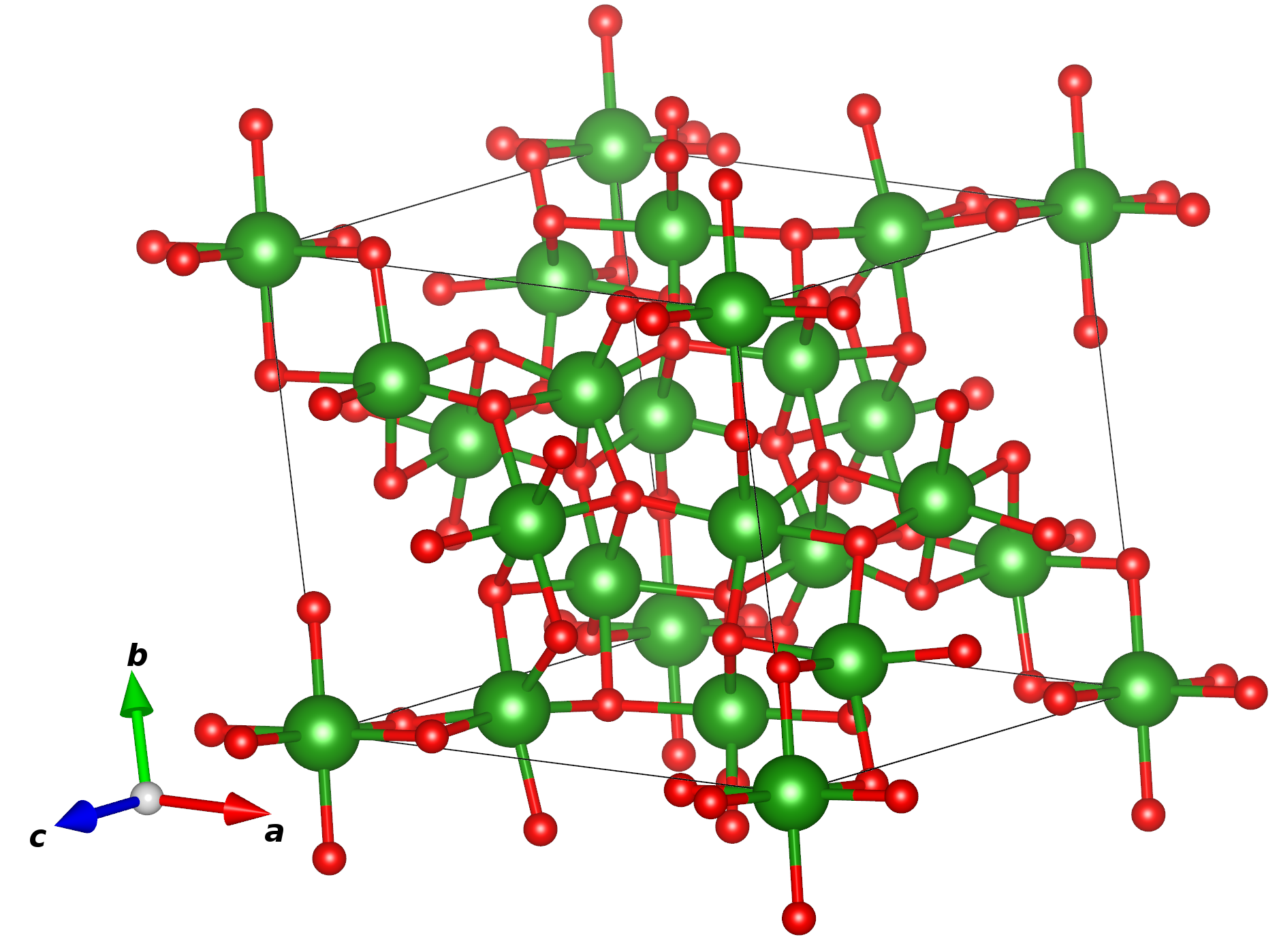
In2O3 can occur in several polymorphs Fuchs and Bechstedt (2008); here we focus on the most stable structure, which is cubic bixbyite, with space group #206 or . Its unit cell, shown in Fig. 2 Momma and Izumi (2011), consists of 40 atoms. We obtain a lattice parameter of 10.15 Å, in good agreement with the experimental value of 10.12 Å Marezio (1966). Since there are 40 atoms in the unit cell, 120 phonon modes are present, which significantly increases the computational burden of calculating the electron-phonon interactions on a fine q-point mesh. Our calculated frequencies at the point agree well with previous calculations Garcia-Domene et al. (2012) and with experiment Garcia-Domene et al. (2012); Kranert, Schmidt-Grund, and Grundmann (2014); White and Keramidas (1972); Korotcenkov et al. (2005); Matei Ghimbeu, Schoonman, and Lumbreras (2008); Zhang et al. (2007); Berengue et al. (2010); Rojas-López et al. (2000). A comparison of the Raman-active phonon frequencies is shown in the Supplementary Material in Table S1.
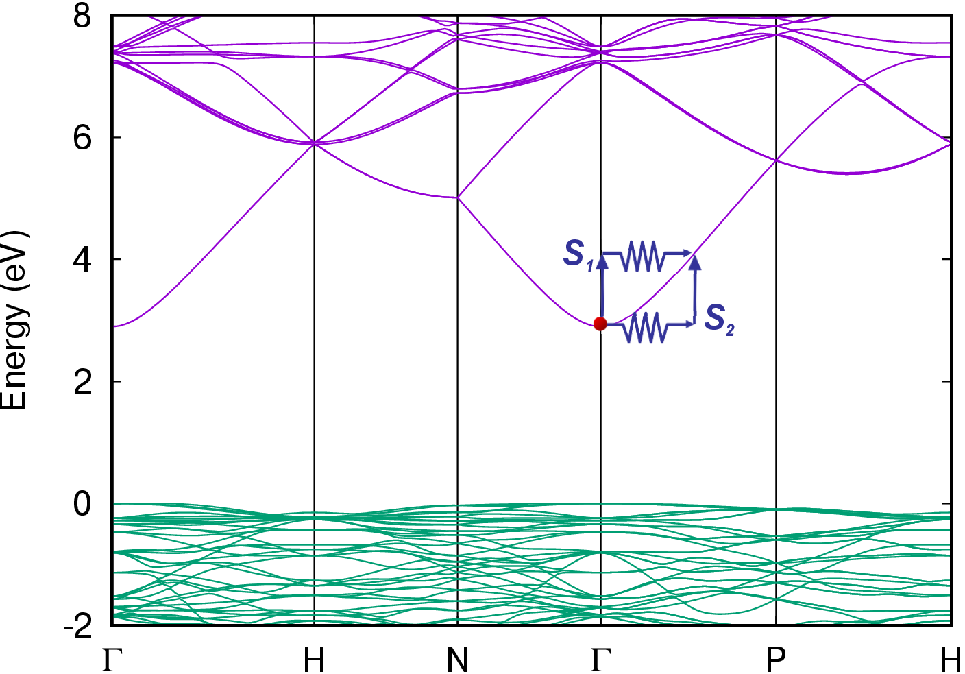
The electronic band structure is shown in Fig. 1. Since LDA underestimates the band gap, a scissor shift is applied to the conduction bands to reproduce the experimental band gap. However, since we are only considering free-carrier absorption here, the exact value of the band gap is not important; what matters is the conduction-band structure. To ascertain the validity of the LDA conduction-band structure, we compared it with a calculation performed with a hybrid functional Heyd, Scuseria, and Ernzerhof (2006). The energy and dispersion of conduction bands were very similar in the two calculations, with differences that would have negligible effects on the calculated free-carrier absorption [see Fig. S1 of the Supplementary Material]. Figure 1 shows that the conduction-band minimum is located at the point. The valence bands have low dispersion and mainly O character, while the lowest conduction band is comprised of orbitals and has a large dispersion. The electron effective mass calculated from LDA, 0.16 , is close to the experimental value of 0.18 Feneberg et al. (2016).
Phonons mediate absorption by providing the momentum necessary to reach unoccupied conduction-band states away from the zone center. We describe this indirect absorption process using Fermi’s golden rule Peelaers, Kioupakis, and Van de Walle (2015):
| (1) | |||||
is the unit-cell volume, and are the energy and polarization of the absorbed photon, the refractive index of In2O3 at frequency , the phonon energy, and the electron energy. and indicate the band number, the phonon mode, and the wave vectors, and and are the number of and wave vectors in the grid. The generalized optical matrix elements and are given by
| (2) |
and correspond to the two possible paths of the indirect absorption process (see Fig. 1). are the optical matrix elements and the electron-phonon coupling matrix elements. The factor accounts for the carrier and phonon statistics and contains the temperature dependence,
| (3) |
Here and are the phonon and electron occupation numbers. The upper (lower) sign corresponds to phonon emission (absorption). Note that all quantities entering here are calculated from first principles, without any fitting parameters. Eq.(1) contains a sum over both k- and q-points. By making the assumption that all free carriers are located near the point, and that these have similar electron-phonon matrix elements, we can replace the double sum by a single sum over q-points, which is essential for rendering the computations tractable. The assumption that the carriers are located near the point is fully justified for electron concentrations up to cm-3, while the assumption for the matrix elements is valid for Fermi levels up to at least 0.5 eV above the conduction-band minimum (corresponding to carrier concentrations up to cm-3). To obtain results that are independent of the free-carrier concentration, we will report the absorption cross section, which is the absorption coefficient divided by the free-carrier concentration.
There are two possible processes: either an existing phonon can be absorbed or a new phonon can be emitted. Our results (at 300 K) are shown in Fig. 3 for photon energies up to 3.7 eV, the energy at which strong absorption from valence to conduction bands sets in. However, weak across-the-gap absorption has been observed with an onset at the fundamental gap; Weiher and Ley (1966); Irmscher et al. (2014) therefore we shade the energy range between 2.9 and 3.7 eV in grey. The phonon emission process is clearly the dominant absorption process at 300 K. This also implies that lowering the temperature would not significantly affect phonon-assisted absorption, since phonons can be emitted even at 0 K. Fig. S2 shows a comparison between 0 K and 300 K.
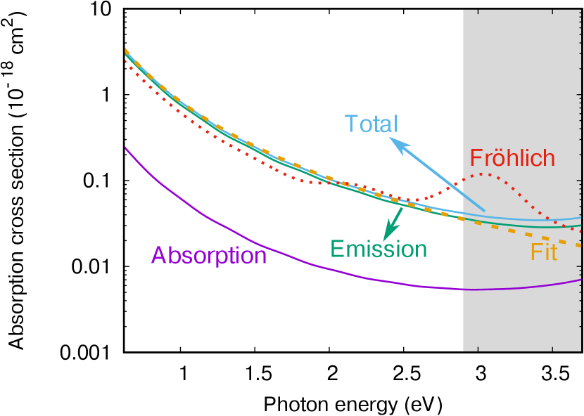
The indirect absorption increases with decreasing photon energy (or longer photon wavelength). We find that the relation between phonon-assisted indirect absorption and photon energy can be expressed by a power law. In Fig. 3 we show a fit to , where we fitted in the region of photon energies from 0.62 eV to 2.7 eV. The fit yields a coefficient = 0.83. The agreement between the first-principles results and the fit is very good at low photon energies; deviations are observed only for photon energies larger than 2.5 eV. This fit implies that the absorption is inversely proportional to the cube power of the photon energy, or equivalently proportional to the cube of the photon wavelength. Such a relationship is expected in the case of linear dispersion (a good approximation for conduction bands that show strong nonparabolicity) and absorption dominated by longitudinal-optical (LO) phonons Peelaers, Kioupakis, and Van de Walle (2012).
Our first-principles results in Fig. 3 take all phonon modes and all possible transitions between electronic bands into account. It is informative to compare these results with a simplified model, in which we assume that the main contribution to phonon-assisted absorption is due to LO phonon modes, and that only the highest phonon mode contributes. The electron-phonon coupling matrix elements are then given by the Fröhlich model
| (4) |
where is the frequency of the LO mode at the point and and are the high-frequency and static dielectric constants. For photon energies up to about 2 eV, where intraband transitions dominate, the single-LO phonon mode Fröhlich model closely approximates the full first-principles results. The slight underestimation is related to the fact that not all modes are taken into account. Nevertheless, the good agreement indicates that LO phonon modes, with a dependence of the electron-phonon matrix elements, are dominant.
The absorption cross section calculated by the Fröhlich model shows a slight upturn at energies just below 2 eV, which is caused by interband processes: an inspection of the band structure (Fig. 1) shows that at energies of about 2 eV above the conduction-band minimum the first conduction band becomes degenerate with the second conduction band, for example along the segment H-N. However, the Fröhlich model overestimates the magnitude of these interband electron-phonon matrix elements, which is even more evident for interband transitions around 3 eV.
The Fröhlich model also provides insight into why phonon-assisted indirect absorption in In2O3 is about 50% smaller compared to SnO2, Peelaers, Kioupakis, and Van de Walle (2012, 2015) another TCO material. Based on Eq. (4), we see that electron-phonon coupling is stronger in SnO2. SnO2 is more ionic than In2O3, i.e., there is a larger difference between the static and high-frequency dielectric constants and hence the factor in the Fröhlich model [Eq. (4)] is larger in SnO2. In addition, the highest LO phonon frequency in SnO2 is larger than the highest LO frequency in In2O3. Both effects contribute to SnO2 having stronger absorption than In2O3. However, an even larger role is played by the density of states [which enters Eq. (1) through the energy-conserving delta function] being larger in SnO2 than in In2O3, due to the smaller effective mass for electrons of In2O3.
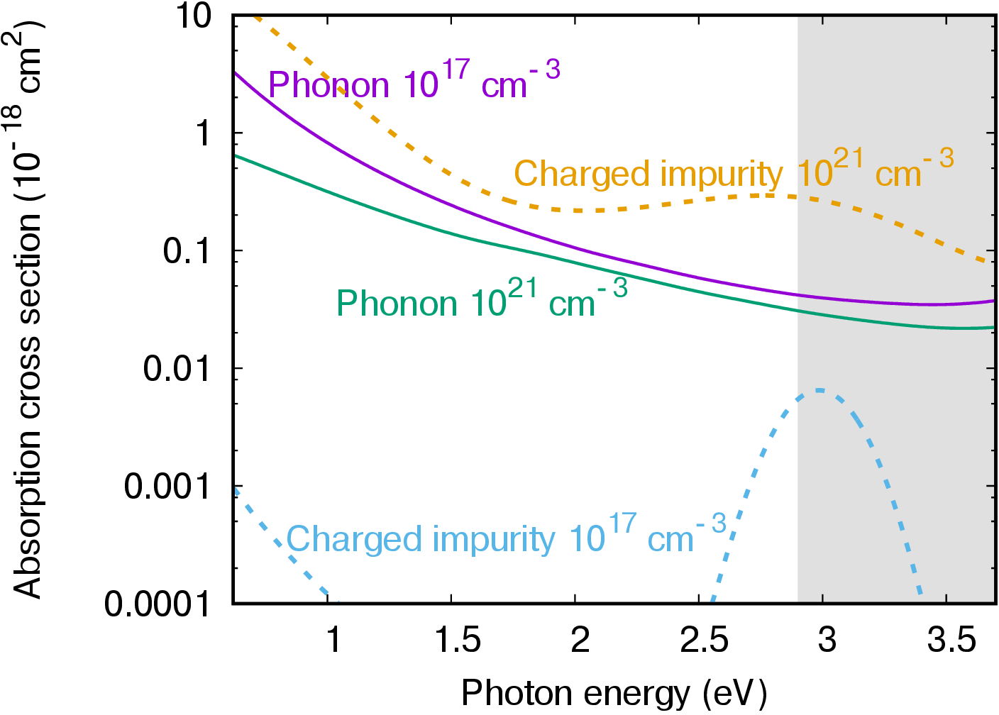
At high carrier concentrations, screening of the electron-phonon interaction can be significant. This effect is included by multiplying the electron-phonon matrix elements by . is a screening length, which is obtained from either the Debye model (non-degenerate case) or the Thomas-Fermi model (degenerate case). Results are shown in Fig. 4 for two values of the electron concentration. The curve labeled “Phonon 1017 cm-3” in Fig. 4 is practically equivalent to the unscreened result (shown previously in Fig. 3), since for these low carrier concentrations the effect of screening is negligible. At higher free-carrier concentrations, screening becomes important, reducing the phonon-assisted absorption cross section. The screening effect is larger for smaller photon energies.
We now turn to a discussion of free-carrier absorption assisted by a different mechanism, namely charged-impurity scattering. This process is unavoidable, because the high conductivity of a TCO requires doping, which leads to the presence of ionized defects or impurities. In In2O3, the free carriers are typically provided by Sn doping, leading to the presence of charged Sn+ centers. We describe the resulting indirect absorption process by scattering off a screened Coulomb potential, where the matrix elements are given by
| (5) |
We assume here that all Sn dopants are ionized and that these are the only charged impurities present; the concentration of ions is then equal to the concentration of free carriers. This assumption neglects compensation and thus provides a lower limit for the total concentration of charged centers.
As seen in Fig. 4, at 1017 cm-3, charged-impurity-assisted absorption is negligible compared to the phonon-assisted process, but at 1021 cm-3, charged-impurity scattering dominates. For photon energies up to 2 eV the absorption decreases with increasing photon energies, similar to the phonon-assisted process. Above 2 eV, the impurity-assisted absorption increases, with a peak around 3 eV. As mentioned before, for energies around 2 eV above the conduction-band minimum, the first conduction band becomes degenerate with the second conduction band (Fig. 1). The corresponding matrix elements are larger for the charged-impurity process compared to the phonon process, leading to an increase in absorption. In addition, around 3 eV, many more final states become available (see, e.g., the band crossings at the H point in Fig. 1). Note that in the band structure obtained using hybrid functionals (see Fig. S1) the higher conduction bands are located at slightly higher energies compared to our LDA calculations; this will move the aforementioned peaks to higher energies. The crossover point, where the impurity-assisted process is similar in magnitude to the phonon-assisted process, occurs at an impurity concentration around 31020 cm-3; at higher doping concentrations impurity-assisted process becomes the dominant absorption process.
In conclusion, we have reported a detailed analysis of the limitations on transparency due to indirect free-carrier absorption in In2O3. Using first-principles techniques, we find that the phonon-assisted process is dominated by emission of phonons, and increases with decreasing photon energies. This increase can be described by a third power dependence on the wavelength. For long-wavelength photons, a Fröhlich model, only taking the highest LO phonon mode into account, provides a reasonable description of the indirect absorption up to about 2.5 eV. This model can also explain why phonon-assisted indirect absorption in In2O3 is about 50% smaller than this in SnO2. Charged-impurity-assisted absorption becomes the dominant process for concentrations above 31020 cm-3.
Supplementary Material
See supplementary material for a comparison of the band structure calculated with LDA and with a hybrid functional, a comparison of the calculated Raman-active phonon frequencies with previous calculations and experiments, and a comparison of the phonon-assisted indirect absorption at 0 K and 300 K.
Acknowledgments
This work was supported by the GAME MURI of the Air Force Office of Scientific Research (FA9550-18-1-0479). Computational resources where provided by the Extreme Science and Engineering Discovery Environment (XSEDE), which is supported by National Science Foundation grant number ACI-1548562.
References
- Ellmer (2012) K. Ellmer, Nat. Photonics 6, 809 (2012).
- Katayama (1999) M. Katayama, Thin Solid Films 341, 140 (1999).
- Fortunato et al. (2007) E. Fortunato, D. Ginley, H. Hosono, and D. C. Paine, MRS Bull 32, 242 (2007).
- Bierwagen (2015) O. Bierwagen, Semicond. Sci. Technol. 30, 024001 (2015).
- Hamberg and Granqvist (1986) I. Hamberg and C. G. Granqvist, J. Appl. Phys. 60, 123 (1986).
- Liu et al. (2014) X. Liu, J. Park, J. H. Kang, H. Yuan, Y. Cui, H. Y. Hwang, and M. L. Brongersma, Appl. Phys. Lett. 105 (2014).
- Peelaers et al. (2015) H. Peelaers, D. Steiauf, J. B. Varley, A. Janotti, and C. G. Van de Walle, Phys. Rev. B 92, 085206 (2015).
- Weiher and Ley (1966) R. L. Weiher and R. P. Ley, J. Appl. Phys. 37, 299 (1966).
- Janowitz et al. (2011) C. Janowitz, V. Scherer, M. Mohamed, A. Krapf, H. Dwelk, R. Manzke, Z. Galazka, R. Uecker, K. Irmscher, R. Fornari, M. Michling, D. Schmeißer, J. R. Weber, J. B. Varley, and C. G. Van de Walle, New J. Phys. 13, 085014 (2011).
- Scherer et al. (2012) V. Scherer, C. Janowitz, A. Krapf, H. Dwelk, D. Braun, and R. Manzke, Appl. Phys. Lett. 100 (2012.
- King et al. (2009) P. D. C. King, T. D. Veal, F. Fuchs, C. Y. Wang, D. J. Payne, A. Bourlange, H. Zhang, G. R. Bell, V. Cimalla, O. Ambacher, R. G. Egdell, F. Bechstedt, and C. F. McConville, Phys. Rev. B 79, 205211 (2009).
- Walsh et al. (2008) A. Walsh, J. Da Silva, S.-H. Wei, C. Körber, A. Klein, L. Piper, A. DeMasi, K. Smith, G. Panaccione, P. Torelli, D. Payne, A. Bourlange, and R. Egdell, Phys. Rev. Lett. 100, 167402 (2008).
- Morris and Monserrat (2018) A. J. Morris and B. Monserrat, Phys. Rev. B 98, 161203 (2018).
- Bierwagen and Speck (2014) O. Bierwagen and J. S. Speck, Phys. Status Solidi A 211, 48 (2014).
- Ceperley and Alder (1980) D. Ceperley and B. Alder, Phys. Rev. Lett. 45, 566 (1980).
- Perdew and Zunger (1981) J. P. Perdew and A. Zunger, Phys. Rev. B 23, 5048 (1981).
- Troullier and Martins (1991) N. Troullier and J. L. Martins, Phys. Rev. B 43, 1993 (1991).
- Giannozzi et al. (2009) P. Giannozzi, S. Baroni, N. Bonini, M. Calandra, R. Car, C. Cavazzoni, D. Ceresoli, G. L. Chiarotti, M. Cococcioni, I. Dabo, A. Dal Corso, S. de Gironcoli, S. Fabris, G. Fratesi, R. Gebauer, U. Gerstmann, C. Gougoussis, A. Kokalj, M. Lazzeri, L. Martin-Samos, N. Marzari, F. Mauri, R. Mazzarello, S. Paolini, A. Pasquarello, L. Paulatto, C. Sbraccia, S. Scandolo, G. Sclauzero, A. P. Seitsonen, A. Smogunov, P. Umari, and R. M. Wentzcovitch, J. Phys. Condens. Matter 21, 395502 (2009).
- Monkhorst and Pack (1976) H. Monkhorst and J. Pack, Phys. Rev. B 13, 5188 (1976).
- Baroni et al. (2001) S. Baroni, S. de Gironcoli, A. Dal Corso, and P. Giannozzi, Rev. Mod. Phys. 73, 515 (2001).
- Fuchs and Bechstedt (2008) F. Fuchs and F. Bechstedt, Phys. Rev. B 77, 155107 (2008).
- Marezio (1966) M. Marezio, Acta Crystallogr. 20, 723 (1966).
- Garcia-Domene et al. (2012) B. Garcia-Domene, H. M. Ortiz, O. Gomis, J. A. Sans, F. J. Manjón, A. Muñoz, P. Rodríguez-Hernández, S. N. Achary, D. Errandonea, D. Martínez-García, A. H. Romero, A. Singhal, and A. K. Tyagi, J. Appl. Phys. 112 (2012.
- Kranert, Schmidt-Grund, and Grundmann (2014) C. Kranert, R. Schmidt-Grund, and M. Grundmann, Phys. Status Solidi Rapid Res. Lett. 8, 554 (2014).
- White and Keramidas (1972) W. B. White and V. G. Keramidas, Spectrochim. Acta A 28, 501 (1972).
- Korotcenkov et al. (2005) G. Korotcenkov, V. Brinzari, M. Ivanov, A. Cerneavschi, J. Rodriguez, A. Cirera, A. Cornet, and J. Morante, Thin Solid Films 479, 38 (2005).
- Matei Ghimbeu, Schoonman, and Lumbreras (2008) C. Matei Ghimbeu, J. Schoonman, and M. Lumbreras, Ceramics International 34, 95 (2008).
- Zhang et al. (2007) Y. Zhang, J. Li, Q. Li, L. Zhu, X. Liu, X. Zhong, J. Meng, and X. Cao, Scripta Materialia 56, 409 (2007).
- Berengue et al. (2010) O. M. Berengue, A. D. Rodrigues, C. J. Dalmaschio, A. J. C. Lanfredi, E. R. Leite, and A. J. Chiquito, J. Phys. D: Appl. Phys. 43, 045401 (2010).
- Rojas-López et al. (2000) M. Rojas-López, J. Nieto-Navarro, E. Rosendo, H. Navarro-Contreras, and M. A. Vidal, Thin Solid Films 379, 1 (2000).
- Momma and Izumi (2011) K. Momma and F. Izumi, J. Appl. Crystallogr. 44, 1272 (2011).
- Heyd, Scuseria, and Ernzerhof (2006) J. Heyd, G. E. Scuseria, and M. Ernzerhof, J. Chem. Phys. 124, 219906 (2006).
- Feneberg et al. (2016) M. Feneberg, J. Nixdorf, C. Lidig, R. Goldhahn, Z. Galazka, O. Bierwagen, and J. S. Speck, Phys. Rev. B 93, 045203 (2016).
- Peelaers, Kioupakis, and Van de Walle (2015) H. Peelaers, E. Kioupakis, and C. G. Van de Walle, Phys. Rev. B 92, 235201 (2015).
- Irmscher et al. (2014) K. Irmscher, M. Naumann, M. Pietsch, Z. Galazka, R. Uecker, T. Schulz, R. Schewski, M. Albrecht, and R. Fornari, Phys. Status Solidi A 211, 54 (2014).
- Peelaers, Kioupakis, and Van de Walle (2012) H. Peelaers, E. Kioupakis, and C. G. Van de Walle, Appl. Phys. Lett. 100, 011914 (2012).