Role of the V-V dimerization in insulator-metal transition and optical transmittance of pure and doped VO2 thin films
Abstract
Insulator to metal (IMT) transition (Tt 341 K) in the VO2 accompanies transition from an infrared (IR) transparent to IR opaque phase. Tailoring of the IMT and associated IR switching behavior can offer potential thermochromic applications. Here we report on effects of the W and the Tb doping on the IMT and associated structural, electronic structure and optical properties of the VO2 thin film. Our results show that the W doping significantly lowers IMT temperature ( 292 K to 247 K for 1.3% W to 3.7% W) by stabilizing the metallic rutile, , phase while Tb doping does not alter the IMT temperature much and retains the insulating monoclinic, , phase at room temperature. It is observed that the W doping albeit significantly reduces the IR switching temperature but is detrimental to the solar modulation ability, contrary to the Tb doping effects where higher IR switching temperature and solar modulation ability is observed. The IMT behavior, electrical conductivity and IR switching behavior in the W and the Tb doped thin films are found to be directly associated with the spectral changes in the V 3 states.
pacs:
64.60.av, 71.23.Cq, 71.15.-m, 71.27.+aI Introduction
Vanadium dioxide (VO2) is known to undergo first order insulator to metal transition (IMT) from the low temperature monoclinic insulating phase to the high temperature rutile metallic phase around the transition temperature Tt 341 K. Structural transformation of VO2 from the rutile, , structure to the monoclinic, structure transforms the equally spaced V atoms, oriented along the rutile axis, into paired (dimerized) and tilted V atoms in the monoclinic structure Zylbersztejn and Mott (1975); Imada et al. (1998); Adler (1968). The IMT in VO2 is accompanied by dramatic modification in optical properties like switching in transmittance/reflectance of the infrared radiations with the insulating phase being transparent to the IR while the metallic phase blocks them. This property of VO2 is potentially useful for designing the thermochromic smart windows which can serve as the best energy management devices as these windows switch the solar heat gain Zhou et al. (2013a); Wu et al. (2013); Zhao et al. (2014).
Changes in the IR and visible transmittance of the VO2 thin films across the IMT can be explained in terms of changes in the band structures, explained in context of the Goodenough model Goodenough (1971); Goodenough and Hong (1973). According to this model, in the rutile metallic phase of the VO2 the octahedral crystal field splits the V 3 degenerate orbitals into doubly degenerate and triply degenerate orbitals. The orbitals are further splitted into the doubly degenerate orbitals and the single (d∥) orbital. Both the and states hybridize with O 2 orbitals to form anti-bonding and molecular orbitals while the d∥ orbitals are oriented along the rutile - axis. In the insulating phase pairing and the tilting of the Vanadium atoms along the rutile - axis results in splitting of the d∥ orbitals into filled bonding and empty anti-bonding orbitals. Band gap of 0.65 eV in the VO2 insulating phase arises due to energy difference between the bonding V 3 and the bands while in the metallic phase energy gap vanishes due to overlapping of the non bonding 3 and the bands at the Fermi level. Decrease in the IR transmittance of the VO2 with increase in the temperature is directly associated with vanishing of the VO2 insulating band gap ( 0.65 eV) and increase in the free carrier concentration in the high temperature metallic phase. Optical transitions in the visible spectral range occur between lower O 2 valence states to the conduction bands Dietrich et al. (2017); Gavini and Kwan (1972).
For practical applications of the VO2 material as thermochromic smart windows, the IMT temperature of the VO2 requires to be tailored down to the room temperature (RT). Chemical doping of electron rich valence shell metal ions viz W6+, Mo6+ and Nb6+ and optimizing the amount of strain in epitaxial VO2 thin films have been found effective ways to reduce the Tt of the VO2 to the room temperature Batista et al. (2011); Patridge et al. (2012); Tan et al. (2012); Dietrich et al. (2017); Muraoka and Hiroi. (2002). Doping of electron doped ions Tungsten (W6+), have been found effective in reducing the transition temperature to RT, while doping of the hole doped Terbium ions (Tb3+), has not significant impact on the transition temperature lowering Wang et al. (2016). There is always a trade off between the transition temperature reduction, solar modulation ability and the luminous transmittance in the VO2 thin films. Normally an increase in the luminous transmittance is accompanied by the decrease in the solar modulation Hu et al. (2016); Burkhardt et al. (2002). W doping is found to reduce the solar modulation ability and the luminous transmittance Burkhardt et al. (2002) while Tb doping enhances the luminous transmittance accompanied with the decrease in the solar modulation ability Wang et al. (2016). Two systems (W and Tb doped VO2) show contrast effect on the electrical and optical properties of the VO2 thin films. It is essential to completely study both the W and the Tb VO2 systems and explore the role of W and Tb in modifying the VO2 IMT and optical properties.
We have synthesized the pure VO2 and W (1.3%, 2.9% and 3.7%) & Tb (1.3%, 3.3% and 4.6%) doped VO2 thin films on the quartz substrates using the pulsed laser deposition technique. By combining structural, electrical, optical and electronic structure studies we present an insightful of the effects of the W and Tb doping on the IMT and optical properties of the VO2. Our results directly show the doping induced alterations to the V-V dimerization in the VO2 thin film, on which electrical and optical properties are largely dependent.
II Experimental details
KrF excimer laser ( = 248 nm, repetition rate of 5Hz and pulse energy of 210 mJ) was focused onto a target (pressed pure and W & Tb doped V2O5) with a fluence of 1.1 mJ/cm2. Ultrasonically cleaned quartz substrates were maintained at a temperature of 700∘C during the deposition. All depositions were performed in an oxygen partial pressure of 10 m Torr. X-ray diffraction (XRD) was carried out with a Bruker D8 x-ray diffractometer with Cu K radiation. Temperature dependent resistivity measurements were performed in the standard four point configuration. Temperature dependent Raman spectra were collected in backscattering geometry using a 10 mW Ar (475 nm) laser as an excitation source coupled with a Labram-HRF micro-Raman spectrometer equipped with a 50X objective. The X-ray photoelectron spectroscopy (XPS) measurements were performed using an Omicron energy analyzer (EA-125) with a Al Kα (1486.6 eV) X-ray source. Soft X-ray absorption spectroscopy (SXAS) across the V and the O edges were carried out in the total electron yield (TEY) mode at the beam line BL-01, Indus-2 at RRCAT, Indore, India. Energy resolution during SXAS measurements at the oxygen edge energy was 250 meV. Bulk VO2 was measured for reference. V-K edge X-ray absorption near edge spectroscopy (XANES) measurements were performed at beamline P64, PETRA III, DESY, Hamburg, Germany in fluorescence mode. Optical transmittance spectra were collected using UV-VIS-NIR spectrometer, Perkin Elmer USA Model: Lambda 950, operating in the spectral range of 175 to 3300 nm having resolution 0.02 nm (UV-VIS) and 0.2 nm (NIR). Doping % used throughout the paper are calculated using the XPS spectra of the Tb and the W.
III Results and Discussions
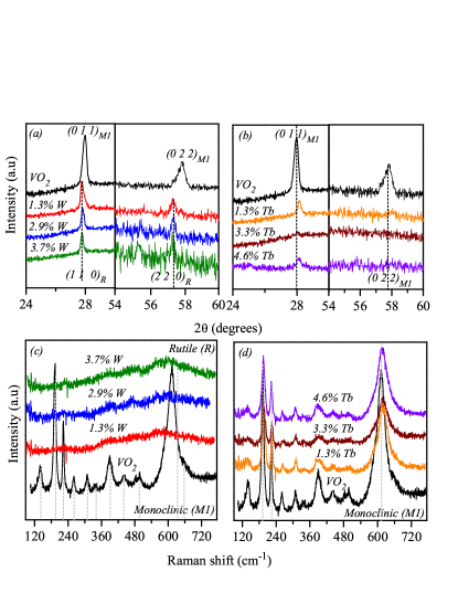
Figure 1 (a) shows X-ray diffraction (XRD) of the pure and W doped thin films. XRD confirms growth of the VO2 monoclinic () phase in the undoped thin film, visualized from the diffraction peaks observed at 2 27.97 ∘ and 57.79 ∘ corresponding to the reflections from the VO2 monoclinic (0 1 1) and (0 2 2) planes respectively Majid et al. (2018); Sepúlveda et al. (2008). Tungsten doped VO2 thin films are grown in the rutile () phase, evident from 2 positions of the diffraction peaks at 27.78 ∘ and 57.27 ∘, which correspond to reflections from the rutile (1 1 0) and (2 2 0) planes, respectively Sepúlveda et al. (2008). Further confirmation about grown phases in the pure and the W doped VO2 thin films comes from the Raman spectra shown in the Figure 1 (c). Pure VO2 thin film shows seven Ag and three Bg Raman modes at 139, 192, 222, 309, 337, 389, 613 cm-1 and 260, 441, 496, 659 cm-1, respectively, which belongs to the VO2 monoclinic, M1, phase Shibuya and Sawa (2017). The Ag symmetry Raman modes and at 192 and 222 cm-1 are assigned to the V-V vibrations while rest of the observed Raman peaks are related to V-O vibrations Marini et al. (2008); Chen (2011). Complete disappearance of the vibrational modes observed in all the W doped thin films confirm growth of the rutile phase, consistent with earlier reports Majid et al. (2018); Ji et al. (2014). XRD patterns of the Tb doped thin films shown in the Figure 1 (b) exhibit slight decrease in crystalline nature and shifting of the monoclinic, , (0 1 1) diffraction peak towards higher 2, compared to the pure VO2 thin film. Shifting of the diffraction peaks to higher 2 values with increase in the Tb doping % is attributed to decrease in unit cell size of the VO2. Raman spectra shown in the Figure 1 (d) further confirms growth of the monoclinic, , phase in the Tb doped thin films and substantiates to XRD results. In contrast to the W doping and no phase transformation is visualized due to the Tb doping.
| sample | Tt (K) | (K) | (K) | IMT strength | ∥ intensity |
|---|---|---|---|---|---|
| resistivity | Raman | Transmittance | resistivity | XAS | |
| VO2 | 340.1 | 322.3 | 320.7 | 56.6 | 0.55 |
| 1.3% W | 292.2 | 241.8 | 285.2 | 21.4 | 0.42 |
| 2.9% W | 275.8 | 198.9 | 246.2 | 18.8 | 0.45 |
| 3.7% W | 247.3 | 122.5 | 217.1 | 11.1 | 0.46 |
| 1.3% Tb | 339.2 | 329.3 | 341.6 | 271.4 | 0.64 |
| 3.3% Tb | 335.7 | 328.2 | 338.5 | 142.5 | 0.62 |
| 4.6% Tb | 335.5 | 322.3 | 330.5 | 109.9 | 0.66 |
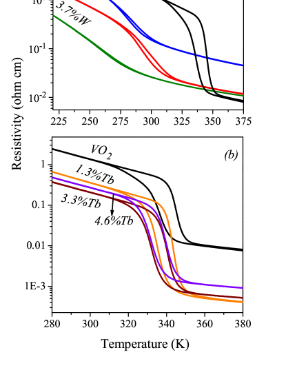
Temperature dependent resistivity () measurements of the pure and the W/Tb doped VO2 thin films are shown in the Figures 2 (a) and 2 (b). The characteristic IMT is observed in all the thin films. To infer quantitative information from temperature dependent resistivity measurements, the IMT in all the thin films were fitted by the Boltzmann function ( = 1 - equation (1)). is the resistivity, (), T0 is the transition temperature and dT signifies the transition width. IMT temperature (Tt) is defined as an average of transition temperatures measured in the cooling and the heating cycles. The IMT temperature for the pure and the doped VO2 thin films are illustrated in the Table I. Tungsten doping has effectively reduced the IMT transition temperature of the VO2 thin film. In the 1.3% W doped VO2 thin film IMT is observed near at room temperature ( 292 K), which is consistent with the earlier reports Takami et al. (2012); Shibuya et al. (2010). Tb doping has small impact on the IMT temperature of the VO2 thin film compared to the W doping. Resistivity measurements are also used to calculate the IMT strength defined as resistivity ratio (Tt-)/ (Tt+). Calculated values of the IMT strength of the pure and the doped VO2 thin films are listed in the Table I.
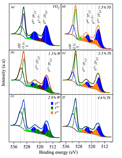
For correct estimation of chemical states of the Vanadium and the dopant elements we have carried out XPS measurements, shown in the Figure 3. XPS of the pure VO2 thin film (Figure 3 (a)) confirms the +4 oxidation state of the Vanadium, which is visible from the binding energy positions of the spin-orbit split features V 2 516 eV and V 2 523 eV. The features at 531.3 eV, 530 eV and 527 eV correspond to the OH concentration, O 1 and the V 23/2 satellite peak, respectively Zimmermann et al. (1998); Silversmit et al. (2004). The spectral feature at 520 eV is assigned to V1+/2+ oxidation state which may arises due to reduction of some of the V4+ due to the oxygen deficiency. W doping (Figures 3 (b and c)) induces the spectral features at binding energies 514 eV and 522 eV, belonging to 23/2 and 21/2 states, while Tb (Figures 3 (d, e and f)) doping results in the inclusion of 23/2 and 21/2 states at the binding energy values 517 eV and 524 eV.
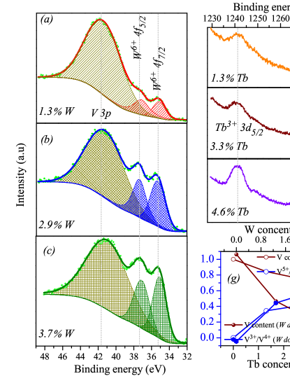
XPS spectra shown in the Figures 4 (a-c) confirm the +6 oxidation state of the W which is evident from the binding energy positions of 47/2 35 eV and 45/2 37 eV features, while the Figures 4 (d-f) represent +3 oxidation state of the Tb which is visualized from the spectral features at 1241 eV and 1276 eV belonging to Tb 35/2 and 33/2 states. The feature at 41.5 eV is due to V 3 states Pan et al. (2017); Zhang et al. (2012). In order to maintain charge neutrality in the W and the Tb doped VO2 thin films, some Vanadium atoms change their oxidation state to +3 and +5 to compensate the higher () and the lower (Tb3+) charge states. Figure 4 (g) shows decrease in the Vanadium content with increase in the doping percentage of the W and the Tb atoms and the decrease in the Vanadium content is found to be accompanied by an increase in the ratio of / and / for W and Tb doped VO2, respectively.
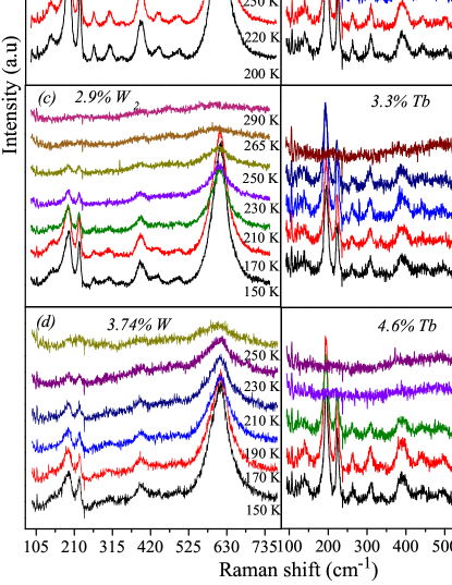
Temperature dependent Raman spectra of the pure and the W/Tb doped VO2 thin films are shown in the Figures 5 (a-g), measured in the cooling cycles. Temperature dependent structural transition form the low temperature monoclinic () structure to the high temperature rutile () structure is observed in all the thin films without presence of any intermediate structures ( and ) which are usually accessible via chemical doping in the VO2 Majid et al. (2018). Temperature dependent frequency position of the Raman mode , of the pure and the W/Tb doped VO2 thin films are plotted in the Figures 5 (h) and (i). There is not any anomalous change observed in the temperature dependent frequency position of the Raman mode, . Softening of the Raman mode positions due to lattice thermal expansion is accompanied by large and sudden change at the structural transition temperature. In the Tb doped VO2 thin films frequency shift of the mode from 613 cm-1 (observed in the Pure VO2 thin film, to 619 cm-1) reflects significant influence of the Tb doping on the V-O vibrational mode compared to the W doping, where the mode stays around 613 cm-1. Normally the higher frequency shift of the mode position in the pure VO2 thin film is considered as fingerprint for identification of the VO2 and structures Majid et al. (2018); Atkin et al. (2012); Marini et al. (2008), however in the Tb doped VO2 thin films higher frequency shift of the mode to 619 cm-1 is much less compared to that observed for the phase ( 629 cm-1) and for the phase ( 642 cm-1).
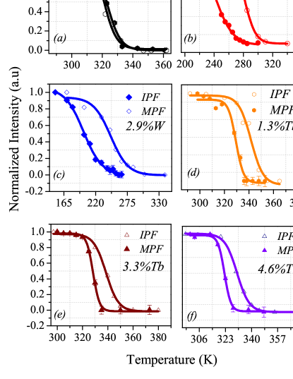
Recently, Yoav et al.,Kalcheim et al. (2019) used XRD and IR spectroscopic techniques to understand coupling between the IMT and the structural phase transition in the V2O3 thin films and discussed the non reliability of the resistance measurements in determination of the correct insulating and the metallic phase fractions. We have extracted the the monoclinic phase fraction (MPF) and the insulating phase fraction (IPF) from temperature dependent Raman and optical transmittance spectra (discussed later, see Figure 7), respectively. Following formula has been used to calculate the IPF (in the range, 2000 to 2500 ).
| (1) |
where and are transmittance of the pure insulating and the pure metallic phases and is the transmittance at temperature, T. The calculated IPF of the pure and the W/Tb doped VO2 thin films are compared with the monoclinic phase fraction (MPF) obtained from temperature dependent integrated intensity of the Raman mode in the Figures 6 (a to f). Calculated transition temperatures, Toc and Tsc from the optical transmittance measurement and the Raman spectroscopy data using the equation (1), are listed in the Table I. In the pure VO2 thin film IMT is found to be coupled with the structural transition while W and Tb doping are found to stabilize the rutile structure prior to the metallic state. Impact of the W doping in the rutile structure stabilization is much more significant compared to the Tb doping.
For thermochromic applications optical properties of the pure and the doped VO2 thin films are characterized using temperature dependent UV-VIS-NIR transmittance spectra shown in the Figure 7. The spectral transmittance in the wavelength range of 250 nm to 2500 nm of the pure (Figure 7 (a)), W doped (Figures 7 (b-d)) and the Tb doped (Figures 7 (e-g)) VO2 thin films are used to calculate the solar transmittance,. For the luminous transmittance, , calculations spectral range 382 nm to 732 nm is used. Both the solar and the luminous transmittance are calculated using following formula:
| (2) |
where Tr() is the spectral transmittance at wavelength . sol () is the solar spectral irradiance for the sun standing 37∘ above the horizon (for the air mass 1.5) and the lum is the standard luminous efficiency function for the photopic vision of human eyes Kang et al. (2010); Zhao et al. (2014). Using the integrated solar and the luminous transmittance, we can calculate the solar and the luminous modulation of the pure and the doped VO2 thin films using following formulas:
| (3) |
| (4) |
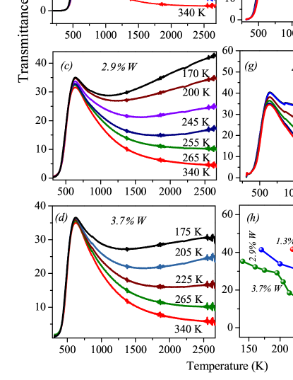
where Tr(sol,I), Tr(sol,M), Tr(lum,I) and Tr(lum,M) are the solar and the luminous transmittance of the insulating and the metallic states, respectively. Parameters obtained from transmittance spectra of the pure and the W/Tb doped VO2 thin films are illustrated in the Table II. IR switching in the pure and the W/Tb doped VO2 thin films can be visualized from the Figure 7 (h) where temperature dependent change in the IR transmittance at the wavelength, 2500 nm is plotted, in the cooling cycle. The IR switching transition temperatures for the pure and the W/Tb doped VO2 thin films are calculated from the IR transmittance Vs T curve, measured in the cooling cycle, using the equation (1) and is found equivalent to (see Table I). The near room temperature Toc, Tr(lum) 40% and the 10% are considered as the best criteria for the VO2 thin films to be employed in thermochromic windows applications Li et al. (2012); Zhao et al. (2014). From the Table II it is found that the W doping in the VO2 thin film effectively reduces the IR switching temperature to near room temperature 282 K (measured in the cooling cycle) but is accompanied with decrease in the solar modulation ability, consistent with earlier reports Granqvist (2007); Hu et al. (2016). With the Tb doping IR switching occurs at higher Toc, while the solar modulation ability is maintained around 15% which is much large compared to the earlier report on Tb doped VO2 thin films Wang et al. (2016). There is always a trade off between the solar modulation ability and the luminous transmittance in the VO2 thin films i.e., an increase in the luminous transmittance is accompanied by the decrease in the solar modulation Hu et al. (2016); Burkhardt et al. (2002). However, in the Tb doped VO2 thin films increase in the luminous transmittance is accompanied with the good and stable solar modulation ability (see Table II).
In order to understand the transmittance observations it is essential to calculate band gap of the pure and the W/Tb doped VO2 thin films corresponding to the visible and the IR transparency, which can be extracted from the Tauc plot shown in the Figures 8 (a) and (b). Tauc plot is graphical description between ()n Vs obtained from the Tauc’s equation Tauc and Menth (1972) given as:
| (5) |
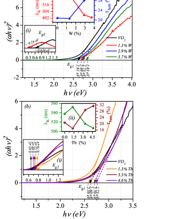
where n = 1/2, 1/3, 2 and 2/3 for the indirect allowed, indirect forbidden, direct allowed and direct forbidden optical transition, respectively, is absorption coefficient obtained from the transmittance spectra, A is a constant and is the photon energy. Usually, in the optical experiments direct band gap is visualized because of the lower excitation probability among different symmetry points during the optical transition Liu et al. (2010).The band gap is obtained by extrapolating the linear portion of the curve while y ordinate is zero. Two types of band gaps are observed i.e., and . corresponds to energy gap between the V 3 and bands while the is due to the optical transition between the O 2 and bands Wan et al. (2017); Li et al. (2013) (Figures 8 (a) and (b)). The IR switching temperature in all the thin films is found to depend on the energy band gap . The lowering of the IR switching temperature in the W doped VO2 thin films (see Table II) is attributed to decrease in the energy band gap, , from 0.63 eV in the pure to 0.24 eV in the 1.3% W doped VO2 thin film, while in the Tb doped VO2 thin films we have observed highest IR switching temperature 341.6 K in the 1.3% Tb doped VO2 thin film having the largest band gap 0.74 eV.
The band gap corresponds to the luminous transparency of the thin films, higher the value higher will be the visible transparency Wan et al. (2017); Li et al. (2013); Zhou et al. (2013b). Inset () of the Figures 8 (a) and (b) show the variation of the luminous transmittance along with the absorption edge (K), obtained from the derivative of the transmittance spectra. The blue shift in the absorption edge along with an increase in the luminous transmittance in the VO2 thin film due to W and Tb doping are found to be consistent with an increase in the energy band gap values .
| sample | Tlum,I | Tlum,M | Tlum | Tsol,I | Tsol,M | Tsol |
|---|---|---|---|---|---|---|
| VO2 | 20.8 | 19.5 | 1.3 | 32.4 | 17.0 | 15.4 |
| 1.3% W | 20.6 | 19.4 | 1.2 | 30.2 | 16.4 | 13.7 |
| 2.9% W | 28.1 | 26.4 | 1.67 | 32.7 | 23.4 | 9.2 |
| 3.7% W | 30.9 | 30.8 | 0.07 | 32.6 | 26.6 | 5.9 |
| 1.3% Tb | 17.1 | 14.9 | 2.2 | 28.9 | 13.6 | 15.2 |
| 3.3% Tb | 28.8 | 26.1 | 2.6 | 38.9 | 23.7 | 15.1 |
| 4.6% Tb | 31.4 | 27.9 | 3.5 | 38.8 | 25.4 | 13.4 |
In the following we will discuss about origin of doping induced changes in the electrical conductivity and optical properties of the VO2. The V edge X-ray absorption spectra of the pure and the W/Tb doped VO2 thin films are shown in the Figure 9 (a). The vanadium spectrum arises due to the transition from the V 2 core level (spin orbit splitted V 2 and 2) to the unoccupied V 3 states and consists of two pronounced features at 518.8 eV (L3) and 525.5 eV (L2). The features at 516.0 eV and 522.6 eV are due to the transitions to crystal field splitted t2g part of the V 3 states Haverkort et al. (2005); Zaanen et al. (1985). The energy positions of the 518.8 eV and 525.5 eV features confirm 4+ oxidation state of the Vanadium. With the W and Tb doping in the VO2 thin film the slight shift in the energy positions of the and states is observed which is due to the additional V3+ and V4+ states created by the W and Tb doping, as inferred from the XPS measurements also.
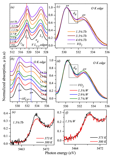
The O edge spectrum, see the Figure 9 (b), results from transition of the O 1 electrons to the vacant O 2 states which are hybridized with the V 3 orbitals and form the conduction band. Peaks at 530.3 eV and 532.8 eV are due to transitions into the and the hybridized bands Ruzmetov et al. (2007); Goodenough and Hong (1973). Doping of the W has clearly resulted in shift of the band towards the lower energies as compared to the pure VO2 thin film which signify the stabilization of the metallic state. The Tb doping shifts the band towards higher energy signifying the stabilization of the insulating state. The crystal field splitting energy (ECF) which is the energy separation between the and the states is found to vary with the W and the Tb doping. Variations in the crystal field splitting energy values due to the W and the Tb doping in the VO2 thin film is also susceptible to different extent of V-V interactions. In order to clearly visualize the spectral changes among the XAS spectra of pure and doped VO2 thin films we have carried out the normalization and horizontal shift of the states to 532.8 eV as shown in the Figures 9 (c and d). The asymmetry observed in the bands around 531 eV, which is marked in both the Figures 9 (c and d), is assigned to the unoccupied d∥ states Ruzmetov et al. (2008); Yeo et al. (2015) and a decrease and an increase in the intensity of the d∥ feature is observed in the W and Tb doping, respectively. For better visualization and comparison pure VO2 spectra is shown in dotted line. The integrated intensity of the d∥ states for the pure and the doped VO2 thin films is noted in the Table 1. The orbitals in the VO2 thin film point in between the ligands and have less orbital overlap with the O 2 orbitals, while the orbitals are directed toward the ligand having a higher overlap with the O 2 orbitals. Therefore, spectral weight of the band is highly sensitive to the V-V interactions while spectral weight of the band is related to the direct V-O interactions Ruzmetov et al. (2008). The pre-edge structures at 5468.3 eV from the V edge XAS observed in the 1.3% Tb and the W doped VO2 thin films at the temperatures 330 K and 373 K are shown in the Figures 9 (e) and (f). The pre-edge peak intensity is highly sensitive to the local geometrical structure around the absorbing atom (V) and increases directly with increase in distortion of the regular octahedral VO6 units Majid et al. (2018). The VO2 rutile, phase has less distorted octahedron compared to the monoclinic, phase, hence an increase in intensity in the 300 K spectra compared to the 370 K spectra of the Tb doped VO2 thin film represent the transition from the phase to the phase while no such signature is observed in the W doped VO2 thin film indicating stable rutile phase at the room temperature and 373 K. By combining the resistivity and XAS measurements we find that the IMT strength of the pure and the W/Tb doped VO2 thin films is directly related to the unoccupied spectral weight of the V 3 states. W doping is found to decrease the IMT strength while Tb doping increases the IMT strength which is accompanied by decrease and an increase in the spectral weight of the V 3 states (see the Table I and the Figure 9 (c)).
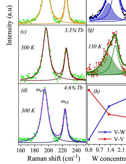
Spectral weight of the states observed in the XAS measurements is directly related to the Vanadium-Vanadium dimerization along the rutile axis Koethe et al. (2006); Quackenbush et al. (2016). The V-V dimerization in the VO2 can be directly visualized from the and the vibrational modes in Raman spectra shown in the Figures 10 (a to g) as both these modes are assigned to V-V vibrations and the frequency mode gives the twisting vibration of the Vanadium dimers along the rutile axis. Raman mode in the pure and the Tb doped VO2 thin films is fitted with a single Lorentzian while in the W doped VO2 thin films vibrational mode is fitted with two Lorentzian peaks at 186 and 195 cm-1. The additional peak at the lower frequency value 186 cm-1 is assigned to the V-W vibrational mode as effective mass of the V-W system is larger as compared to the V-V system. Presence of the V-W vibrational modes in the W doped VO2 thin films signify replacement of the V atoms by the doped W atoms along the VO2 rutile axis, hence the loss of V-V dimerization. On contrary in the Tb doped VO2 thin film absence of any such extra mode signify that the Tb is not doped along the rutile axis therefore there is no loss of V-V dimerization. Figure 10 (h) shows the intensity variation of the V-V and the V-W vibrational modes in the W doped sample. Increase in intensity of the V-W vibrational mode and corresponding decrease in intensity of the V-V vibrational mode with increase in the W doping can be visualized. According to Tang et al.,Tang et al. (1985) electron dopant W atoms break the V4+-V4+ dimers and result in formation of the V3+-W6+ and V3+-V4+ pairs along the rutile axis due to electron transfer from the W to the V ions. The electronic charge transfer from the W atoms resulting in formation of V3+ ions (see Figure 3) stabilizes the metallic state and the loss of the Vanadium dimerizations favors the rutile symmetry Tan et al. (2012); Tang et al. (1985). Band filling due to electron dopant W atoms results in stabilization of the metallic phase by melting down the electron-electron correlations, U, Takami et al. (2012).
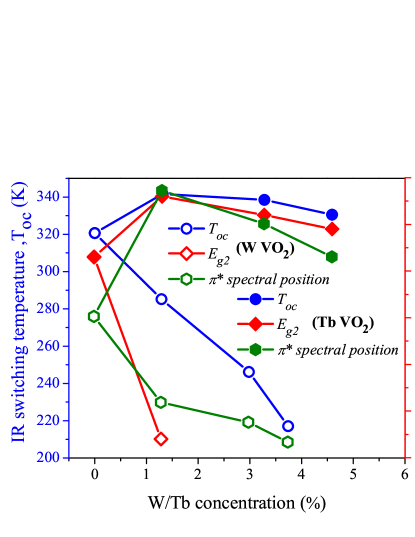
XAS and optical transmittance results reveal that the IR switching temperature, Toc is strongly related to the spectral weight and position of the V 3 and states (see Figure 9). Infrared switching temperature (Toc) in all thin films, which is sensitive to the energy gap Eg2 (energy gap between the and the states) is found to be directly related to the spectral position of the states (see Figure 11). The spectral weight and position of the band is directly sensitive to the V-V interactions and reflects the extent of the V-V hybridization Ruzmetov and Ramanathan. (2010). Larger V-V hybridization will stabilize the bonding states and simultaneously shift the anti-bonding states towards the higher photon energy. The decreasing Toc & Eg2 with increasing W doping concentration and increasing Toc & Eg2 with increasing Tb concentration are found to be concomitant with shift of the states spectral weight towards lower and higher energies, respectively. The solar modulation ability of all the thin films can be directly associated with their IMT strength. In the W doped VO2 thin films decreases with decrease in the IMT strength. In the Tb doped VO2 thin films an increased and the stabilized values (contrary to previous report Wang et al. (2016)) can be attributed to an increased IMT strength observed from the resistivity measurements. Hence the solar modulation ability, , is found to be largely dependent on stabilization of the VO2 monoclinic, phase and therefore on preservation of the V-V dimers.
IV Conclusions
In summary, changes in electrical, structural, optical and electronic structure properties of the pure and the W/Tb doped VO2 thin films have been studied. Electron dopant W atoms are found to significantly reduce the IMT temperature in the VO2 thin film by stabilizing the rutile metallic phase, contrary to the hole dopant Tb atoms which favor and stabilize the insulating monoclinic phase. Loss of the V-V dimerization is clearly observed due to the W doping while the Tb doping is found to strengthen the V-V dimerization. Loss of the V-V dimerization has been found to directly influence the spectral weight of the V 3 states, a decrease and an increase in spectral weight of the states has been observed due to the W and the Tb doping, respectively. Changes in strength of the IMT, the electrical conductivity, the IR switching temperature and the solar modulation ability due to the W and Tb doping are found directly related to the spectral changes in the states. Conclusions which are directly related to thermochromic applications of doped VO2 thin films are as follows, i) A decrease in the IR switching temperature is observed due to the W doping while an increase in the IR switching temperature is visualized due to the Tb doping. Near room temperature IR switching temperature ( 285 K, cooling cycle) is observed at an optimum 1.3% W concentration. ii) An increase in the luminous transmittance is observed for both, the W and the Tb doping. Luminous transmittance of 30.9% and 31.4% is observed for the highest 3.7% W and 4.6% Tb dopings. iii) An increased and stabilized solar modulation ability ( 15.2) is observed with the 1.3% Tb doping and a decrease in the solar modulation ability ( 13.7) due to an optimum 1.3% W doping. Our results also clearly indicate that the W and the Tb co-doping may be a potential candidate to get a combination of lowered IMT temperature, large and high essential for smart window applications.
V Acknowledgments
Authors are thankful to Sharad Karwal Rakesh Sah and Ajay Rathore for help during XPS, XAS and Raman measurements, respectively. R.J. Choudhary is gratefully acknowledged for providing the PLD setup. E. Welter is gratefully acknowledged for his support during hard X-ray absorption spectroscopy measurements, performed under India-DESY collaboration. K.G. thanks, Council of Scientific and Industrial Research, New Delhi, India, for support in form of SRF. D.K.S. acknowledges support from SERB, India, in the form of an early-career research award (ECR/2017/000712).
References
- Zylbersztejn and Mott (1975) A. Zylbersztejn and N. F. Mott, Phys. Rev. B 11, 4383 (1975).
- Imada et al. (1998) M. Imada, A. Fujimori, and Y. Tokura, Rev. Mod. Phys. 70, 1039 (1998).
- Adler (1968) D. Adler, Rev. Mod. Phys. 40, 714 (1968).
- Zhou et al. (2013a) J. Zhou, Y. Gao, Z. Zhang, H. Luo, C. Cao, Z. Chen, L. Dai, and X. Liu, Sci. Rep. 3 (2013a).
- Wu et al. (2013) C. Wu, F. Feng, and Y. Xie, Chem. Soc. Rev. 42, 5157 (2013).
- Zhao et al. (2014) L. Zhao, L. Miao, C. Liu, C. Li, T. Asaka, Y. Kang, Y. Iwamoto, S. Tanemura, H. Gu, and H. Su, Sci. Rep. 4, 7000 (2014).
- Goodenough (1971) J. B. Goodenough, J. Solid State Chem. 3, 490 (1971).
- Goodenough and Hong (1973) J. Goodenough and H. Y. Hong, Phys. Rev. B 8, 1323 (1973).
- Dietrich et al. (2017) M. K. Dietrich, F. Kuhl, A. Polity, and P. J. Klar, Appl. Phys. Lett. 110, 141907 (2017).
- Gavini and Kwan (1972) A. Gavini and C. C. Kwan, Phys. Rev. B 5, 3138 (1972).
- Batista et al. (2011) C. Batista, J. Carneiro, R. Ribeiro, and V. Teixeira, J. Nanosci. Nanotechnol. 11, 9042 (2011).
- Patridge et al. (2012) C. J. Patridge, L. Whittaker, B. Ravel, and S. Banerjee, J. Phys. Chem. C 116, 3728 (2012).
- Tan et al. (2012) X. Tan, T. Yao, R. Long, Z. Sun, Y. Feng, H. Cheng, X. Yuan, W. Zhang, Q. Liu, C. Wu, et al., Sci. Rep. 2, 466 (2012).
- Muraoka and Hiroi. (2002) Y. Muraoka and Z. Hiroi., Appl. Phys. Lett. 80, 583 (2002).
- Wang et al. (2016) N. Wang, M. Duchamp, R. E. Dunin-Borkowski, S. Liu, X. Zeng, X. Cao, and Y. Long, Langmuir 32, 759 (2016).
- Hu et al. (2016) L. Hu, H. Tao, G. Chen, R. Pan, M. Wan, D. Xiong, and X. Zhao, J. Sol-Gel Sci. Technol. 77, 85 (2016).
- Burkhardt et al. (2002) W. Burkhardt, T. Christmann, S. Franke, W. Kriegseis, D. Meister, B. Meyer, W. Niessner, D. Schalch, and A. Scharmann, Thin Solid Films 402, 226 (2002).
- Majid et al. (2018) S. Majid, D. Shukla, F. Rahman, S. Khan, K. Gautam, A. Ahad, S. Francoual, R. Choudhary, V. Sathe, and J. Strempfer, Phys. Rev. B 98, 075152 (2018).
- Sepúlveda et al. (2008) N. Sepúlveda, A. Rúa, R. Cabrera, and F. Fernández, Appl. Phys. Lett. 92, 191913 (2008).
- Shibuya and Sawa (2017) K. Shibuya and A. Sawa, J. Appl. Phys. 122, 015307 (2017).
- Marini et al. (2008) C. Marini, E. Arcangeletti, D. Di Castro, L. Baldassare, A. Perucchi, S. Lupi, L. Malavasi, L. Boeri, E. Pomjakushina, K. Conder, et al., Phys. Rev. B 77, 235111 (2008).
- Chen (2011) X.-B. Chen, J. Kor. Phys. Soc. 58, 100 (2011).
- Ji et al. (2014) Y. Ji, Y. Zhang, M. Gao, Z. Yuan, Y. Xia, C. Jin, B. Tao, C. Chen, Q. Jia, and Y. Lin, Sci Rep 4 (2014).
- Takami et al. (2012) H. Takami, T. Kanki, S. Ueda, K. Kobayashi, and H. Tanaka, Phys. Rev. B 85, 205111 (2012).
- Shibuya et al. (2010) K. Shibuya, M. Kawasaki, and Y. Tokura, Appl. Phys. Lett. 96, 022102 (2010).
- Zimmermann et al. (1998) R. Zimmermann, R. Claessen, F. Reinert, P. Steiner, and S. Hüfner, J. Phys.: Condens. Matter 10, 5697 (1998).
- Silversmit et al. (2004) G. Silversmit, D. Depla, H. Poelman, G. B. Marin, and R. De Gryse, J. Electron Spectrosc. Relat. Phenom. 135, 167 (2004).
- Pan et al. (2017) G. Pan, J. Yin, K. Ji, X. Li, X. Cheng, H. Jin, and J. Liu, Sci. Rep. 7, 6132 (2017).
- Zhang et al. (2012) Y. Zhang, W. Li, M. Fan, F. Zhang, J. Zhang, X. Liu, H. Zhang, C. Huang, and H. Li, J. Alloys Compd. 544, 30 (2012).
- Atkin et al. (2012) J. M. Atkin, S. Berweger, E. K. Chavez, M. B. Raschke, J. Cao, W. Fan, and J. Wu, Phys. Rev. B 85, 020101 (2012).
- Kalcheim et al. (2019) Y. Kalcheim, N. Butakov, N. M. Vargas, M.-H. Lee, J. del Valle, J. Trastoy, P. Salev, J. Schuller, and I. K. Schuller, Phys. Rev. Lett. 122, 057601 (2019).
- Kang et al. (2010) L. Kang, Y. Gao, Z. Zhang, J. Du, C. Cao, Z. Chen, and H. Luo, J. Phys. Chem. C 114, 1901 (2010).
- Li et al. (2012) S.-Y. Li, G. A. Niklasson, and C.-G. Granqvist, Thin Solid Films 520, 3823 (2012).
- Granqvist (2007) C. G. Granqvist, Sol. Energy Mater. Sol. Cells 91, 1529 (2007).
- Tauc and Menth (1972) J. Tauc and A. Menth, J. Non-Cryst. Solids 8, 569 (1972).
- Liu et al. (2010) G.-H. Liu, X.-Y. Deng, and R. Wen, J. Mater. Sci. 45, 3270 (2010).
- Wan et al. (2017) M. Wan, M. Xiong, N. Li, B. Liu, S. Wang, W.-Y. Ching, and X. Zhao, Appl. Surf. Sci. 410, 363 (2017).
- Li et al. (2013) S.-Y. Li, N. R. Mlyuka, D. Primetzhofer, A. Hallén, G. Possnert, G. A. Niklasson, and C. G. Granqvist, Appl. Phys. Lett. 103, 161907 (2013).
- Zhou et al. (2013b) J. Zhou, Y. Gao, X. Liu, Z. Chen, L. Dai, C. Cao, H. Luo, M. Kanahira, C. Sun, and L. Yan, Phys. Chem. Chem. Phys. 15, 7505 (2013b).
- Haverkort et al. (2005) M. Haverkort, Z. Hu, A. Tanaka, W. Reichelt, S. Streltsov, M. Korotin, V. Anisimov, H. Hsieh, H.-J. Lin, C. Chen, et al., Phys. Rev. Lett. 95, 196404 (2005).
- Zaanen et al. (1985) J. Zaanen, G. Sawatzky, J. Fink, W. Speier, and J. Fuggle, Phys. Rev. B 32, 4905 (1985).
- Ruzmetov et al. (2007) D. Ruzmetov, S. D. Senanayake, and S. Ramanathan, Phys. Rev. B 75, 195102 (2007).
- Ruzmetov et al. (2008) D. Ruzmetov, S. D. Senanayake, V. Narayanamurti, and S. Ramanathan, Phys. Rev. B 77, 195442 (2008).
- Yeo et al. (2015) L. Yeo, A. Srivastava, M. Majidi, R. Sutarto, F. He, S. Poh, C. Diao, X. Yu, M. Motapothula, S. Saha, et al., Phys. Rev. B 91, 081112 (2015).
- Koethe et al. (2006) T. C. Koethe, Z. Hu, M. W. Haverkort, C. Schüßler-Langeheine, F. Venturini, N. B. Brookes, O. Tjernberg, W. Reichelt, H. H. Hsieh, H.-J. Lin, et al., Phys. Rev. Lett. 97, 116402 (2006).
- Quackenbush et al. (2016) N. Quackenbush, H. Paik, M. Wahila, S. Sallis, M. Holtz, X. Huang, A. Ganose, B. Morgan, D. O. Scanlon, Y. Gu, et al., Phys. Rev. B 94, 085105 (2016).
- Tang et al. (1985) C. Tang, P. Georgopoulos, M. Fine, J. Cohen, M. Nygren, G. Knapp, and A. Aldred, Phys. Rev. B 31, 1000 (1985).
- Ruzmetov and Ramanathan. (2010) D. Ruzmetov and S. Ramanathan., Thin film metal oxides: fundamentals and applications in electronics and energy (Springer, New York, 2010).