Activation of nominally silent domain wall-localized phonons from GHz to THz
pacs:
Valid PACS appear hereFerroelectric domain walls (DWs) are nanoscale topological defects that can be easily tailored to create nanoscale devices Scott (2007); Tagantsev et al. (2010). Their excitations, recently discovered to be responsible for DW GHz conductivity, hold promise for faster signal transmission and processing speed compared to the existing technology Lee et al. (2003); Scott et al. (2012); Wu et al. (2017). Here we find that DW phonons disperse from GHz to THz frequencies, thus explaining the origin of the surprisingly broad GHz signature in DW conductivity Wu et al. (2017). Puzzling activation of nominally silent DW sliding modes in BiFeO3 Huang et al. is traced back to DW tilting and resulting asymmetry in wall-localized phonons. The obtained phonon spectra and selection rules are used to simulate scanning impedance microscopy, emerging as a powerful probe in nanophononics. The results will guide experimental discovery of the predicted phonon branches and design of DW-based nanodevices.
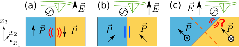
The seminal work of Seidel et al. Seidel et al. (2009) demonstrated that DC conductivity is higher at DWs in BiFeO3 (BFO) than in the bulk, enabling signal transmission along the walls. This inspired a new paradigm for the design of DW-based nanoelectronic devices Catalan et al. (2012); Matsubara et al. (2015); McQuaid et al. (2017); Sharma et al. (2017); Huang and Cheong (2017); Mundy et al. (2017); Turner et al. (2018); Akamatsu et al. (2018); Schaab et al. (2018), leading to demonstration of DW-based diode and transistor operating in kHz range Schaab et al. (2018); McQuaid et al. (2017). The push for higher frequencies, used in modern computers, has led to a discovery of giant increase of the effective DW conductivity at GHz frequencies in recent microwave microscopy experiments Tselev et al. (2016); Wu et al. (2017); Prosandeev et al. (2018). The conductivity results from excitation of soft DW-localized phonon modes, that are at the heart of switching, microwave dielectric loss and dielectric constant enhancement in ferroelectrics Wu et al. (2017); Hlinka et al. (2017). They correspond to oscillations of the DW plane and can be excited by an AC electric field that favors one of the domains during its half period (Fig. 1(a)). Here we show that the frequency of these phonons can go from GHz all the way up to THz, going beyond the frequency range of modern surface acoustic wave-based cell phone transducers.
The results explain why the frequency range of the SMIM anomaly is so wide and reveal DW-localized bands in the phonon spectra of ferroelectrics. We also address the peculiar selection rules for DW excitation. When the ferroelectric polarization component along the driving field is the same in the two domains across the wall, the DW vibration should not be excited (Fig. 1(b)), as seen at 180∘ walls on the face of YMnO3 Wu et al. (2017). However, this rule is violated in recent experiments on rhombohedral BFO, where polarization components along the field across the wall do not differ (Fig. 1(c)), while the DW mode is still excited Huang et al. .
The results could inspire the exploration of DW-based nanosystems in THz frequency range, and lead to novel DW-based phononic nanodevices.
BFO is a rare room-temperature multiferroic with the largest spontaneous polarization among single-phase compounds known to date, and may be soon used in nano-devices Manipatruni et al. (2018). Three types of ferroelectric DWs in the rhomohedral phase are distinguished by the number of polarization components being reversed Marton et al. (2010). The most puzzling data is on R71∘ DWs, at which the component is reversed, and the polarization rotates by across the wall, as seen in Fig. 1(c). R71 DWs are often seen in BFO films grown on a oriented substrate Ziegler et al. (2013); Domingo et al. (2017), such as SrTiO3 and DyScO3. The sliding mode of this wall should not be excited by the field normal to the (100) surface, since neither domain is favored by the field, as seen in Fig. 1(c). However, the impedance signal is still observed experimentally Huang et al. . The important distinction between DWs in YMnO3 and R71 DWs in BFO is their orientation with respect to the surface. YMnO3 DWs are mostly normal to the surface, while BFO R71 DWs are tilted away from the surface normal. In that case the combination of the surface and DW orientations breaks the symmetry, as seen in Fig. 1(c). This symmetry breaking plays a key role in their response to electric fields, even when the simple selection rule, summarised in Fig. 1(a,b), suggests no response.
Results
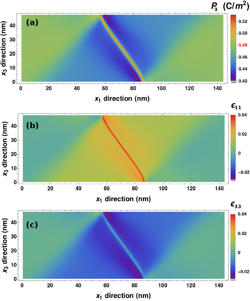
We use the Ginzburg-Landau-Devonshire (GLD) model for DWs in BFO to capture the energetics of interacting ferroelectric polarization and strain (see Methods for details). The DW is tilted 45∘ away from the surface normal and bends near the surface to reduce the DW area, as shown in Fig. 2. Long-range strain textures emanate from the bent segments. decrease in the blue area near the surface is driven by the compression and the tensile strain via electrostriction.
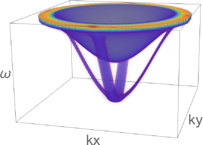
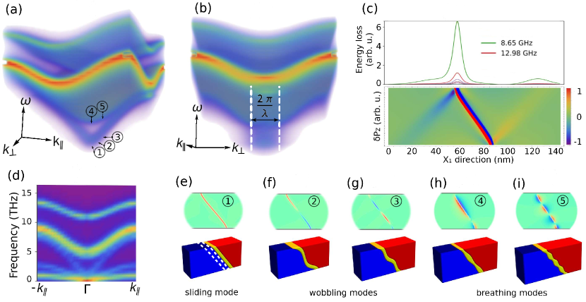
The vibrational modes of the system with DWs are computed from the linearized equations of motion within a discretized Ginzburg-Landau model, and shown in Fig. 3(a,b) (see the Methods section for details). The DW breaks translational invariance and therefore the modes are not characterized by a well-defined quasimomentum. The traditional phonon band structure is then replaced by a spectral function, as seen in Fig. 3(a), where the intensity at frequency and wavevector indicates the content of plane waves with that wavevector in the eigenmodes at that frequency. For a translationally invariant system, sharp peaks would then appear in the spectral function . The long-ranged strain texture of the wall, shown in Fig. 2, is responsible for strong mixing between the DW sliding modes and acoustic phonons.
Fig. 3(a,b) shows the content of plane waves with , while Fig. 3(d) shows the phonon dispersion along the wall. At low frequencies acoustic phonons are observed (their intensity is divided by 10 in Fig. 3(d) to make the DW branch visible). They correspond to strain modulations and mix with modes due to electrostriction, . The V-shaped low frequency branch, marked with (1-3) in Fig. 3(a), extends from around 10 GHz at -point all the way to the bulk polar phonons, and corresponds to the DW sliding and wobbling modes, illustrated in Fig. 3(e-g). The phonons in this branch disperse along the wall (along ), but are localized in the perpendicular direction, and therefore their Fourier components extend to , where stands for the DW width. The intensity of the DW-localized branch is lower than that of the bulk phonons due to the low volume fraction occupied by DWs. The higher frequency modes are the bulk polar phonons.
Fig. 3(e-i) show profiles corresponding to some of the lowest frequency DW sliding modes(e,f,g) and breathing modes (h,i). The nodeless mode shown in the upper panel of Fig. 3(e) corresponds to the increase at the wall during half-period of the oscillation, therefore adding the DW area to the positive domain. During another half-period the negative domain grows. Therefore this mode can be thought of as DW sliding, depicted schematically in the lower panels of Fig. 3(e). A higher energy mode with a node in that branch, shown in the upper panel of Fig. 3(f), corresponds to DW wobbling. The DW breathing modes, schematically shown in Fig. 3(h,i), are found below the band of bulk polar modes, and are indicated with markers (4,5) in Fig. 3(a).
Now we move to the origin of the SMIM signal. In the experiments an AC electric field is applied between the tip and the back electrode, as shown in Fig. 1, and the current is measured. The phonons that have a non-zero energy in the oscillating field of the tip, , are excited and give rise to a displacement current component in phase with the field. The corresponding loss, is measured in addition to the Ohmic losses due to itinerant electrons. The amplitude of a phonon mode with an eigenfrequency is governed by the equation of motion
| (1) |
where the mode is characterized by its effective mass , damping and the spatial polarization profile . The oscillating driving force on the right hand side is due to the electric field of the SMIM tip. Looking for the solution in the form , we obtain the loss power at the tip position ,
| (2) |
The frequency dependence is characterized by a Lorentzian. The integral in the numerator is negligible for phonons whose spatial oscillation period is much smaller that the length scale of the electric field inhomogeneity, roughly determined by the tip radius , therefore the phonons with wavevectors are excited. Fig. 3(c) shows the simulated signal for a BFO sample containing a R71 DW. An asymmetric peak at the DW and a weak signature due to the long-range strain features are visible.
Discussion
Figure 3(c) shows that SMIM conductivity is much higher at DW than in the bulk due to low-frequency DW sliding and wobbling modes. Their dispersion spans the whole GHz range and extends to the bulk polar phonon band, usually positioned at THz frequency. This explains why the GHz microwave conductivity at DWs in hexagonal manganites does not show a narrow peak in frequency domain, but rather rises monotonically towards higher frequencies. The proximity of DW phonons to acoustic branches also leads to phonon scattering and affects thermal conductivity Royo et al. (2017). The low frequency of sliding modes is also behind the giant enhancement of the static dielectric permittivity Hlinka et al. (2017). In addition, soft DW phonons are responsible for mechanical softening phonomena, recently observed in several ferroelectrics Stefani et al. .
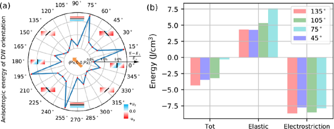
In materials with strong strain-polarization interactions, DWs are aligned into regular lattices by strain fields Artyukhin et al. (2013); Wang et al. (2014), and spectral features similar to the ones in Fig. 3(a,b) are expected. Alternatively, when DWs are randomly oriented, the spectral weigth of DW wobbling and breathing modes spreads along different directions, but the phonon density of states is expected to retain its shape, with the peak at GHz frequencies. The directionality of DWs and their populations in the sample can then be inferred from the orientation and intensity of low-energy branches, as seen in Fig. S2.
The recent observation of nominally silent DW modes in BFO Huang et al. being activated is a surprising evidence that DW type and orientation control local AC conductivity. Possible DW orientations have been classified using symmetry and compatibility analyses Janovec (1976); Fousek and Janovec (1969). In essence, the distances between ionic planes in the two domains must match along the wall. This is only possible for particular DW orientations, for which the strain components in the DW plane match at the wall (see Eq. S3). The energy penalty for violating this condition scales linearly with the wall area, therefore fixing the DW orientation in the bulk. However, in thin films surface strain relaxation allows the DW to deviate from its optimal bulk orientation.
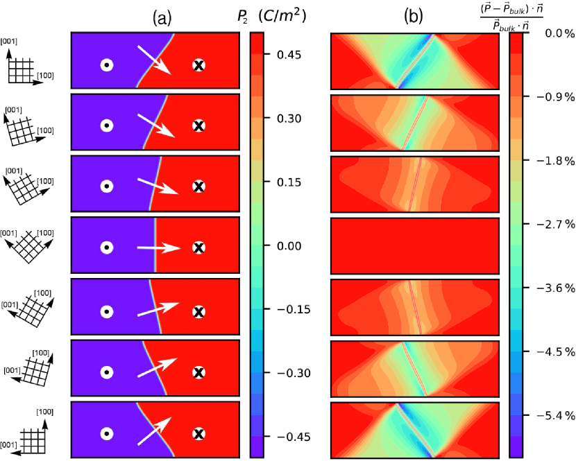
In an infinite bulk sample with a DW, a diagonal mirror plane , shown by the dashed line in Fig. 1(c), is a symmetry operation. This symmetry imposes the requirements: . The surface of the thin film and the domain wall orientation together break this mirror symmetry if they are not orthogonal. The stress at the tilted domain wall then acts on geometrically different regions from the left and right sides of the wall. The resulting asymmetric strain induces asymmetric polarization across the wall via electrostriction Eq. 7. This phenomenon is observed in Fig. 4, where we simulated thin films with different surface orientations with respect to the crystallographic directions (different ways of cutting a film out of a slab). It is seen that the DW orients perpendicular to the direction, and a small bending near the surface is observed in Fig. 4(a) Ishibashi and Salje (2002); Ishibashi et al. (2005); Conti and Weikard (2004); Li et al. (2018). In very thin films, the wall deviates from the orientation towards the surface normal. Fig. 4(b) shows the polarization component normal to the surface. When the wall is tilted at 45∘, the asymmetry of the polarization is evident in Fig. 2(a), especially near the surface where the polarization deviates the most from the bulk value. This asymmetry comes from the asymmetric strain, plotted in Fig. 2(b,c). Even though the DW polarization profile is very narrow, the accompanying strain texture, emanating from the areas of DW bending near the surface Ishibashi and Salje (2002); Ishibashi et al. (2005); Conti and Weikard (2004); Li et al. (2018), extends surprisingly far Salje (1993); Salje et al. (2016), as seen in Fig. 2(b,c).
The polarization asymmetry eventually results in the asymmetry in the phonon polarization profile of the DW sliding mode, as seen in the lower panel of Fig. 3(c). When the polarization interacts with the external electric field, normal to the surface, the electrostatic energy results in a force on the wall due to and excitation of the DW vibration by the SMIM field.
In addition to SMIM, it may be possible to observe the DW-localized modes with inelastic neutron or X-ray scattering, although their intensity may be low due to low volume fraction occupied by DWs. Rapid quenching of a sample across the ferroelectric transition, leading to high DW densities Griffin et al. (2012), or strain-induced generation and alignment of ferroelastic DWs Chae et al. (2012) should increase the intensity of these branches and enable their observation in inelastic neutron scattering experiments and other bulk spectroscopies.
In summary, the simulated phonon spectra reveal the DW-localized phonon branches starting from GHz and extending all the way to THz frequencies. This explains wide frequency range of the conductivity anomaly observed in hexagonal manganites Wu et al. (2017) and other materials. The surprising activation of the nominally silent DW mode at R71∘ DWs in BFO is interpreted in terms of phonon polarization asymmetry due to the interplay of electrostriction and elastic compatibility at a tilted DW. The proposed way to simulate SMIM experiments may be used in emerging second-principles methodologies. Since the low-energy theory used here is rather general, similar phonon spectra must be expected for all ferroic materials, where the order parameter couples strongly to the lattice. We hope this work will motivate the experimental search for DW-localized phonon branches, guide the interpretation of SMIM studies and eventually inspire the development of high-speed DW-based phononic devices, extending surface acoustic wave-based technology to THz DW-based circuits.
References
References
- Scott (2007) J. F. Scott, Science 315, 954 (2007).
- Tagantsev et al. (2010) A. K. Tagantsev, L. E. Cross, and J. Fousek, Domains in Ferroic Crystals and Thin Films (Springer New York, New York, NY, 2010).
- Lee et al. (2003) W. T. Lee, E. K. H. Salje, and U. Bismayer, Journal of Physics: Condensed Matter 15, 1353 (2003).
- Scott et al. (2012) J. F. Scott, E. K. H. Salje, and M. A. Carpenter, Phys. Rev. Lett. 109, 187601 (2012).
- Wu et al. (2017) X. Wu, U. Petralanda, L. Zheng, Y. Ren, R. Hu, S.-W. Cheong, S. Artyukhin, and K. Lai, Sci. Adv. 3, e1602371 (2017).
- (6) Y. L. Huang, L. Zheng, P. Chen, X. Cheng, L. Ponet, R. Ramesh, L. Q. Chen, S. Artyukhin, Y.-H. Chu, and K. Lai, in preparation .
- Seidel et al. (2009) J. Seidel, L. W. Martin, Q. He, Q. Zhan, Y.-H. Chu, A. Rother, M. E. Hawkridge, P. Maksymovych, P. Yu, M. Gajek, N. Balke, S. V. Kalinin, S. Gemming, F. Wang, G. Catalan, J. F. Scott, N. A. Spaldin, J. Orenstein, and R. Ramesh, Nature Materials 8, 229 (2009).
- Catalan et al. (2012) G. Catalan, J. Seidel, R. Ramesh, and J. F. Scott, Rev Mod Phys 84, 119 (2012).
- Matsubara et al. (2015) M. Matsubara, S. Manz, M. Mochizuki, T. Kubacka, A. Iyama, N. Aliouane, T. Kimura, S. L. Johnson, D. Meier, and M. Fiebig, Science 348, 1112 (2015).
- McQuaid et al. (2017) R. G. P. McQuaid, M. P. Campbell, R. W. Whatmore, A. Kumar, and J. M. Gregg, Nature Communications 8, 15105 (2017).
- Sharma et al. (2017) P. Sharma, Q. Zhang, D. Sando, C. H. Lei, Y. Liu, J. Li, V. Nagarajan, and J. Seidel, Sci. Adv. 3, e1700512 (2017).
- Huang and Cheong (2017) F.-T. Huang and S.-W. Cheong, Nature Reviews Materials 2, 17004 (2017).
- Mundy et al. (2017) J. A. Mundy, J. Schaab, Y. Kumagai, A. Cano, M. Stengel, I. P. Krug, D. M. Gottlob, H. Doğanay, M. E. Holtz, R. Held, Z. Yan, E. Bourret, C. M. Schneider, D. G. Schlom, D. A. Muller, R. Ramesh, N. A. Spaldin, and D. Meier, Nature Materials 16, 622 (2017).
- Turner et al. (2018) P. W. Turner, J. P. V. McConville, S. J. McCartan, M. H. Campbell, J. Schaab, R. G. P. McQuaid, A. Kumar, and J. M. Gregg, Nano Letters (2018).
- Akamatsu et al. (2018) H. Akamatsu, Y. Yuan, V. A. Stoica, G. Stone, T. Yang, Z. Hong, S. Lei, Y. Zhu, R. C. Haislmaier, J. W. Freeland, L.-Q. Chen, H. Wen, and V. Gopalan, Phys Rev Lett 120 (2018).
- Schaab et al. (2018) J. Schaab, S. H. Skjærvø, S. Krohns, X. Dai, M. E. Holtz, A. Cano, M. Lilienblum, Z. Yan, E. Bourret, D. A. Muller, M. Fiebig, S. M. Selbach, and D. Meier, Nature Nanotechnology 13, 1028 (2018).
- Tselev et al. (2016) A. Tselev, P. Yu, Y. Cao, L. R. Dedon, L. W. Martin, S. V. Kalinin, and P. Maksymovych, Nature Communications 7, 11630 (2016).
- Prosandeev et al. (2018) S. Prosandeev, Y. Yang, C. Paillard, and L. Bellaiche, npj Comput Mater 4 (2018).
- Hlinka et al. (2017) J. Hlinka, M. Paściak, S. Körbel, and P. Marton, Phys. Rev. Lett. 119 (2017).
- Manipatruni et al. (2018) S. Manipatruni, D. E. Nikonov, C.-C. Lin, B. Prasad, Y.-L. Huang, A. R. Damodaran, Z. Chen, R. Ramesh, and I. A. Young, Sci. Adv. 4, eaat4229 (2018).
- Marton et al. (2010) P. Marton, I. Rychetsky, and J. Hlinka, Phys. Rev. B 81 (2010).
- Ziegler et al. (2013) B. Ziegler, K. Martens, T. Giamarchi, and P. Paruch, Phys. Rev. Lett. 111, 247604 (2013).
- Domingo et al. (2017) N. Domingo, S. Farokhipoor, J. Santiso, B. Noheda, and G. Catalan, Journal of Physics: Condensed Matter 29, 334003 (2017).
- Royo et al. (2017) M. Royo, C. Escorihuela-Sayalero, J. Íñiguez, and R. Rurali, Phys. Rev. Materials 1, 051402 (2017).
- (25) C. Stefani, L. Ponet, K. Shapovalov, P. Chen, M. Stengel, S. Artyukhin, G. Catalan, and N. Domingo, in preparation .
- Artyukhin et al. (2013) S. Artyukhin, K. T. Delaney, N. A. Spaldin, and M. Mostovoy, Nature Materials 13, 42 (2013).
- Wang et al. (2014) X. Wang, M. Mostovoy, M. G. Han, Y. Horibe, T. Aoki, Y. Zhu, and S.-W. Cheong, Phys. Rev. Lett. 112, 247601 (2014).
- Janovec (1976) V. Janovec, Ferroelectrics 12, 43 (1976).
- Fousek and Janovec (1969) J. Fousek and V. Janovec, J Appl Phys 40, 135 (1969).
- Ishibashi and Salje (2002) Y. Ishibashi and E. Salje, Journal of the Physical Society of Japan 71, 2800 (2002).
- Ishibashi et al. (2005) Y. Ishibashi, M. Iwata, and E. Salje, Japanese Journal of Applied Physics 44, 7512 (2005).
- Conti and Weikard (2004) S. Conti and U. Weikard, The European Physical Journal B - Condensed Matter and Complex Systems 41, 413 (2004).
- Li et al. (2018) L. Li, J. R. Jokisaari, Y. Zhang, X. Cheng, X. Yan, C. Heikes, Q. Lin, C. Gadre, D. G. Schlom, L.-Q. Chen, and X. Pan, Advanced Materials 30, 1802737 (2018).
- Salje (1993) E. K. Salje, Phase Transitions in Ferroelastic and Co-elastic Crystals (Cambridge, UK: Cambridge University Press, 1993) p. 296.
- Salje et al. (2016) E. K. H. Salje, O. Aktas, and X. Ding, “Functional topologies in (multi-) ferroics: The ferroelastic template,” in Topological Structures in Ferroic Materials: Domain Walls, Vortices and Skyrmions, edited by J. Seidel (Springer International Publishing, Cham, 2016) pp. 83–101.
- Griffin et al. (2012) S. M. Griffin, M. Lilienblum, K. T. Delaney, Y. Kumagai, M. Fiebig, and N. A. Spaldin, Phys. Rev. X 2, 041022 (2012).
- Chae et al. (2012) S. C. Chae, N. Lee, Y. Horibe, M. Tanimura, S. Mori, B. Gao, S. Carr, and S.-W. Cheong, Phys. Rev. Lett. 108, 167603 (2012).
- Nambu and Sagala (1994) S. Nambu and D. A. Sagala, Phys. Rev. B 50, 5838 (1994).
- Park et al. (2018) S. M. Park, B. Wang, S. Das, S. C. Chae, J.-S. Chung, J.-G. Yoon, L.-Q. Chen, S. M. Yang, and T. W. Noh, Nature Nanotechnology 13, 366 (2018).
- Saj Mohan et al. (2019) M. M. Saj Mohan, S. Bandyopadhyay, T. Jogi, S. Bhattacharya, and R. Ramadurai, Journal of Applied Physics 125, 012501 (2019).
- Alnæs et al. (2015) M. S. Alnæs, J. Blechta, J. Hake, A. Johansson, B. Kehlet, A. Logg, C. Richardson, J. Ring, M. E. Rognes, and G. N. Wells, Archive of Numerical Software 3 (2015).
- Logg et al. (2012) A. Logg, K.-A. Mardal, G. N. Wells, et al., Automated Solution of Differential Equations by the Finite Element Method (Springer, 2012).
- Marton (2018) P. Marton, Phase Transitions 91, 959 (2018).
- Sidorkin (2012) A. S. Sidorkin, Journal of Advanced Dielectrics 02, 1230013 (2012).
- Wang et al. (2011) Y. Wang, J. E. Saal, P. Wu, J. Wang, S. Shang, Z.-K. Liu, and L.-Q. Chen, Acta Materialia 59, 4229 (2011).
- Landau (2004) L. D. Landau, Theory of Elasticity 7 (Elsevier LTD, Oxford, 2004).
Acknowledgements
The authors thank X. Cheng, L.Q. Chen, Y.L. Huang, L. Zheng for stimulating discussions. We acknowledge the CINECA award under the ISCRA initiative, for the availability of high performance computing resources and support. K.L. was supported by US National Science Foundations Award No. DMR-1707372.
Author contributions
P.C. has performed the numerical simulations. P.C. and L.P. implemented and carried out the finite-element calculations on the Landau model and wrote the initial draft of the manuscript, which was finalized by S.A and R.C. with input from all authors. S.A. conceived the project and planned the study.
Competing interests
The authors declare no competing interests.
Methods
In order to elucidate the essential physics that is responsible for the activation of the tilted R71 walls, we use a simplified GLD model Nambu and Sagala (1994). To this end, we focus on the polar mode that connects the parent centrosymmetric phase with the ferroelectric one and consider its interactions with strains (through electrostriction), while neglecting octahedral rotations.
The free energy density, expanded near the centrosymmetric paraelectric parent structure is written as:
| (3) | |||
| (4) | |||
| (5) | |||
| (6) | |||
| (7) | |||
| (8) |
where stands for the components of the ferroelectric polarization; the strain tensor is related to symmetrized gradients of deformations as , where the deformation vector relates points in the reference structure to in the deformed structure; summation over repeated indices is implied. represents the distorted Mexican hat-shaped potential that determines the amplitude and anisotropy of the polarization. describes the energy penalty due to spatial variations of the polarization. describes elastic energy, while is the electrostriction term that refers to the interaction between polarization and strain. The flexoelectric coupling , that describes interactions of strain gradient with the polarization, was also included as in Ref. Park et al. (2018), but does not change the qualitative results reported here. The parameters of the model were adopted from Ref. Saj Mohan et al. (2019). In order to minimize the free energy Eq. 3 we solved the Euler-Lagrange equations with respect to using finite element method as implemented in Fenics software Alnæs et al. (2015); Logg et al. (2012). The real space was discretized with element dimensions 0.4 nm giving rise to a periodic lattice potential acting on the DW, that gaps the sliding mode at 10 GHz Marton (2018). This frequency an order of magnitude higher than characteristic frequencies of DW vibrations due to electrostatic effects Sidorkin (2012). The simulated thin film was 60 nm thick and 180 nm wide, and a single DW was placed in the middle. Test calculations were performed for the 360 nm wide film to validate the long-range strain profile. Zero external stress boundary conditions were applied on the top surface while was used at the bottom one. At the two ends in the direction, both open and twisted boundary conditions were tested to ensure the absence of boundary effects within the domain wall area. Periodic boundary conditions were applied in the translational direction () to mimic an infinite system.
Phonons are computed using 20*1*20 mesh with a single domain wall in the middle. The energy was minimized and the force constants were computed. The mass matrix was adjusted to fit the gap between acoustic and optical bands of the spectrum to DFT calculations Wang et al. (2011).
I Supporting Information
The two polar phases which define neighboring domains have to be mechanically connected by a DW plane described by the normal vector . The spontaneous polarizations and deformations in the two domains are denoted as and respectively, where . Let be a vector in the DW plane within the reference structure. In a polar domain the electrostriction leads to strain, therefore at the boundary of the first domain goes into Landau (2004)
| (S1) |
where the second term on the right-hand side represents a rigid rotation by angle around vector . The third term corresponds to a deformation vector due to the strain tensor . An analogous formula holds for in the second domain. To avoid dislocations and cracks between the two domains, these deformed vectors must match at the DW, . Therefore
| (S2) |
Taking the scalar product with eliminates the vector product term leading to:
| (S3) |
Therefore the strain compatibility requires the strain components in the DW plane to be equal in the two domains across the wall.
In the bulk of each domain, the strain tensor can be obtained from the stress free condition ,
| (S4) |
where . We substitute Eq. S4 into Eq. S3, and take into account that only changes sign across the R71 DW, to obtain . The two solutions are and , the latter meaning that all the vectors in the wall plane are perpendicular to . However, in thin films the violation of the constraint does not lead to infinite elastic energy, and allows the strain to relax at the surface. Therefore, the DW may deviate from the lowest energy orientation in the bulk. To confirm this, we fixed and imposed domain walls in with different orientations , as shown by black lines in the colored slabs in Fig. S1(a). As seen from Fig. S1(b), the DW energy is minimized when the DW normal is parallel to . Note that in the bulk the deviations from the optimal DW orientation are penalized with elastic energy scaling linearly with the DW area. Fig. S1(b) shows that the energy penalty indeed comes from the elastic contribution due to strain mismatch between the domains.