square \affiliation[a]New York University Abu Dhabi, Saadyat Island, Abu Dhabi, UAE \affiliation[b]University College London, London, UK \affiliation[c]Università degli Studi Roma Tre, Rome, Italy \affiliation[d]YahSat Space Lab, Khalifa University of Science and Technology, Abu Dhabi, UAE \affiliation[e]ASI Space Science Data Center (ASI-SSDC), Rome, Italy \affiliation[f]INAF, Osservatorio Astronomico di Roma (INAF-OAR), Monte Porzio Catone (Rome), Italy \emailAddlaura.manenti@nyu.edu \emailAddadriano.digiovanni@nyu.edu
Characterisation of a CeBr3(LB) detector for space application
Abstract
We describe the performance of a low background cerium bromide, CeBr3(LB), scintillator crystal coupled to a Hamamatsu R11265U-200 photomultiplier. This detector will be the building block for a gamma-ray detector array designed to be the payload for a CubeSat to be launched in 2020. The aim of the mission is to study flashes of gamma rays of terrestrial origin. The design of the detector has been tuned for the detection of gamma rays in the – energy range.
Gamma detectors; Photon detectors for UV, visible and IR photons (vacuum); Scintillators and scintillating fibres and light guide; Scintillators, scintillation and light emission processes
1 Introduction
As of June 2019, more than two-thousand CubeSats have already been launched into space [1]. CubeSats are miniature satellites consisting of one standard unit (1U) with dimensions of , weighting about and a power consumption of less than 2 W. CubeSats range from as small as 1U to as big as 12U and may serve different purposes, such as scientific, educational, commercial, military etc. They were first proposed by Professor Jordi PuigSuari at California Polytechnic State University (Cal Poly) and Professor Bob Twiggs at Stanford University’s Space Systems Development Laboratory (SSDL), whose original project, called CubeSat program, was to “develop a picosatellite standard that significantly reduces the cost and development time of student satellites” [2]. This work presents one of the four crystals of an array being planned to operate within 1U of a 3U CubeSat to be launched in 2020 to the International Space Station (ISS), from where it will be deployed into Low-Earth Orbit (LEO). The purpose of this CubeSat mission, temporarily called RAADSat (Rapid Acquisition Atmospheric Detector Satellite), is to detect and study Terrestrial Gamma-Ray Flashes (TGFs).
TGFs are bursts of gamma rays of atmospheric origins (thunderstorms) and can usually be detected by low-Earth orbit satellites [3, 4, 5, 6, 7]. They can also be sporadically observed by detectors on aircraft [8] and at ground level [9, 10]. TGFs were first discovered by the Burst and Transient Source Experiment (BATSE) on the Compton Gamma Ray Observatory (CGRO) in 1994 [3]. BATSE’s primary objective was to study Gamma-Ray Bursts (GRBs), which are events of much longer duration compared to TGFs. BATSE only detected a small number of TGFs over its years of operation (about one event recorded every two months). In fact, the shortest time scale on which BATSE could trigger was , almost three orders of magnitude larger than the average TGF duration, therefore only very bright TGFs could trigger on such a long time scale. The median TGF duration is less than , and TGFs as short as have been reported [11].
Since their discovery [12], it was apparent that TGFs were correlated with thunderstorms, but it was only in 1996 that Inan and Reising [13] provided the first direct evidence that electrical activity was associated with TGFs. Intense radio burst signals of very low frequency (VLF), called “radio atmospherics” or “sferics” [14], typical of natural lightning discharges, were measured at Palmer Station, Antartica, along the CGRO’s footprint [13]. In 2005, the Reuven High Energy Solar Spectroscopic Imager (RHESSI) satellite recorded 86 TGFs over six months [4]. The observed rate corresponded to 50 TGFs globally each day. Currently, assuming nearly dead-time free TGF detection, the expected TGF rate is of about 1500 events globally per day [15].
Even though TGF detection capabilities have substantially improved over the years, the exact mechanism behind TGF production is yet to be fully understood. The current leading model proposed to explain TGFs is the Relativistic Runaway Electron Avalanche (RREA). For thunderstorms with electric fields above V/m, where is the density of air with respect to sea level, an electron gains more energy than what it loses in collisions with air, hence “running away”. Runaway electrons were first theorised by Wilson in his seminal work of 1925 [16], but it was only in 1992 that Gurevich, Milikh and Roussel-Dupré [17] showed that elastic scattering between runaway electrons could initiate a multiplication process, also known as avalanche (apparently, Wilson was also aware of this process which he referred to as “snow ball effect” in his notes [18]). It should be noted that this is not what we conventionally call “electric breakdown” [19], as the process is not self-sustained [20]. In fact, runaway electrons must be continuously provided by an external source (an exception to this is the “cold runaway”, where thermal electrons normally created in thunderstorm discharges may all runaway if the electric field exceeds a critical value of [19]). The two other leading models of TGFs are instead self-sustained mechanisms [21, 22].One is called “relativistic feedback” model, and involves backward propagating runaway positrons and backscattered X-rays [12]; the other, instead, involves the acceleration of electrons in the strong electric field of stepping lightning leaders [23, 24, 25].
All missions before 2018 that have studied TGFs were actually not specifically designed for this scope. BATSE, AGILE (Astro‐rivelatore Gamma a Immagini LEggero), and the Fermi Gamma-Ray Space Telescope aimed at investigating cosmic gamma-ray sources, while RHESSI’s primary goal was to explore solar flares by detecting photons from to . Past missions might have underestimated the intensity of these atmospheric phenomena because their time response was not optimised for these fast phenomena.
One major mission to study TGFs has already begun in 2018 with the installation of the ASIM (Atmosphere-Space Interactions Monitor) on the CEPF (Columbus External Platform Facility) of the ISS [26]. Another mission should start at the end of 2019 with the launch of TARANIS (Tool for the Analysis of Radiation from lightning and Sprites), a satellite designed to specifically observe TGFs and related atmospheric phenomena [27]. The RAADSat would be one of the first satellites built on a low-budget to study TGFs. The mission, whose cost is about half a million USD, is supported by the UAE Space Agency through the 2018 “UAE Minisat Competition”, where the proposed payload has won the first place and has been awarded 100k USD.
For this mission, we propose a fast detector which uses low background cerium bromide (CeBr3(LB)) scintillating crystals (manufactured by Scionix) coupled to fast, compact, and lightweight photomultiplier tubes (PMTs, model R11265U-200 manufactured by Hamamatsu). The detector covers a wide energy range, from up to . Figure 1 shows the layout of the detector, consisting of an array made of basic units, each separately operated and read out, together with an anti-coincidence detector to tag charged particle induced events.
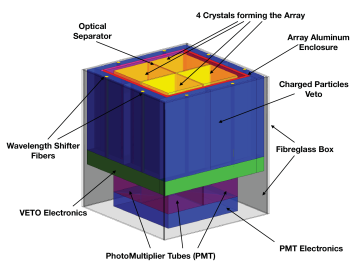
This work reports on the characterisation and preliminary tests of a basic space unit to assess its suitability to operate in space. The unit consists of one CeBr3(LB) crystal coupled to one PMT, leading to an overall volume of and a total weight of . Such configuration will fit into a single (1U) CubeSat unit. Our mission comprises of a 3U CubeSat bus, of which two units will house two almost identical detectors. The third will be dedicated to telemetry, transmission and necessary satellite control subsystems.
It is also worth mentioning that, albeit RAADSat was primarily designed for studying TGFs, it could also serve the HERMES (High Energy Rapid Modular Ensemble of Satellites) project. HERMES is a mission concept based on a swarm of picosatellites in low-Earth orbit to study hard X-ray/soft gamma-ray transients such as GRBs. One of the main objectives of the project is to test quantum space-time by measuring the time delay between GRB gammas of different energies [28]. The picosatellites must be fast scintillators with high-accuracy time resolution. Both requirements are met by the RAADSat.
The paper is organised as follows: in section 2 the scintillator is described and the motivation behind its choice compared to other crystals. Section 3 describes the modification of the PMT voltage divider to comply with the power requirements of the future RAADSat mission. Section 4 presents the measurement of the PMT gain at different high-voltage settings and the energy calibration and resolution characterisation by exposing the detector to a wide spectrum of radioactive gamma emitters. Lastly, section 5 reports on the characterisation of this detector under vacuum at temperatures ranging from about to .
2 The scintillator
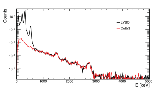
Given the timing characteristics of TGFs, a prerequisite for the detection medium is a short decay time to accommodate high event rates. A crystal which was initially considered as a viable option was the cerium-doped lutetium yttrium orthosilicate (), also abbreviated as LYSO:Ce. LYSO:Ce has a relatively high density ( [29]), good light yield (5600–7600 ph/MeV [29]), good energy resolution, and a decay time of about at [29], with the advantage of not being hygroscopic [30]. However, LYSO:Ce is radioactive because of the presence of 176Lu, which decays via emission. Measurements performed with a NaI:Tl detector (shown in Fig.3) resulted in an estimated total activity forty times higher than that of the CeBr3(LB). For this reason, LYSO:Ce was then discarded.
Another crystal that in recent years has attracted a lot of attention for space-based applications is CeBr3(LB). This crystal has a relatively short decay time () and, contrary to LYSO:Ce, CeBr3(LB) shows a much lower intrinsic radioactivity [31].
| NaI:Tl | LYSO:Ce | CeBr3(LB) | |
| Density [g/cm3] | 3.67 | 7.25 | 5.18 |
| Absolute light yield [photons/MeV] | 38000 | 28000 | 60000 |
| Decay time [ns] | 230 | 40 | 20 |
| Emission Peak [nm] | 415 | 420 | 370 |
| Hygroscopic | yes | no | yes |
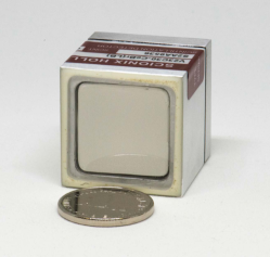
Although CeBr3(LB) is less dense than LYSO:Ce (see Table1 for comparison), resulting in a reduced stopping power, its crystal structure represents a promising material with a very low intrinsic radioactivity and an excellent photon yield (60000 photons/MeV [31]). Hence, we decided to opt for the CeBr3(LB), a sample of which we sourced from Scionix, Ltd (Netherlands). The sample, shown in Fig. 2, has dimensions of and is encapsulated in an aluminium case with overall dimension of . The crystal comes with an optical interface—a thick quartz window—for protection.
According to the manufacturer, the CeBr3(LB) emission spectrum peaks at with a typical decay time of 18–. The peak emission reported by [31] is instead at , while the decay time reported in the same work varies with the size and thickness of the crystal. The scintillation decay time of the crystal used in this work is 23.53 and it has been measured by fitting a sample of 10000 waveforms generated by exposing the detector to a source and acquired by using a LeCroy HDO6104 oscilloscope.
3 The detector unit
We looked for a compact, rugged photomultiplier tube to be coupled to the CeBr3(LB) crystal. The choice fell on the Hamamatsu R11265U-200 series, a sample of which is shown in Fig. 4.
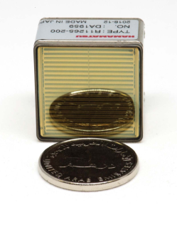
The area of the photocathode window, mm2, matches the quartz window of our CeBr3(LB) crystal, and its limited weight of makes this tube a promising choice for our CubeSat application. The main characteristics of the PMT R11265U-200 are listed in Table 2.
| Dimensions [mm3] | |
|---|---|
| Photocathode | Ultra-bialkali |
| Weight [g] | 31 |
| Peak sensitivity [nm] | 400 |
| Quantum efficiency | 43 % |
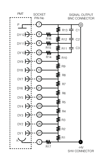
The R11265U-200 PMT provided by Hamamatsu comes with a standard voltage divider (shown in Fig. 5) with a total resistance of . At an operating voltage of , the total power consumption is . For a array, the total required power (due to the voltage dividers only) would be incompatible with the overall power budget of a CubeSat. We have therefore assembled an alternative voltage divider with a total resistance of , which hereafter will be referred as the “10X divider”. The power consumption of the new divider is only . However, the current flowing through the divider should be kept large compared to the current flowing from cathode to anode through the dynodes chain. Especially in correspondence of intense flashes and high rates, the internal current at the peak of a pulse might become comparable to the divider current, causing the voltage between two successive dynodes to deviate from the nominal value and the PMT gain to drift. This effect is particularly important for the dynodes closer to the anode—where the current flowing from one dynode to the other is higher. To avoid PMT gain instability and a nonlinear response, it is common practice to add stabilising capacitors to the last stages of the resistor chain. Such capacitors supply the PMT with an electric charge when the signal pulse is formed, keeping the voltage drop between the dynodes constant. The values of the capacitors placed in parallel in the new divider layout have been modified according to the empirical relation [35]
| (1) |
where C is the value of the stabilising capacitor, I is the current associated to the signal pulse, is the pulse width, and V the voltage across the capacitor. Considering a typical gamma absorption in the crystal, with an average current pulse of the order of , a width of and across the capacitor, a capacitance value of is obtained. Following a conservative approach, a capacitance of has been used for C1, C2, and C3 (see Fig. 5). The performance of the R11265U-200 PMT with the factory voltage divider and the 10X divider has been evaluated and the results are reported in section 4.
| Factory Divider | 10X Divider | |
|---|---|---|
| R1 | ||
| R2 | ||
| R5, R6 | ||
| R7 to R12 | ||
| R13 | ||
| R14 to R16 | ||
| R17 | ||
| C1 | ||
| C2 | ||
| C3 | ||
| RTOT | ||
| Current at V= -1000 V |
4 Detector characterisation at room temperature
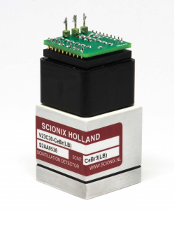
The basic detector unit with the crystal coupled to the PMT is shown in Fig. 6. In the final configuration, the unit will be inserted in a high strength silicone rubber case (Momentive RTV615) for two main reasons: firstly, to prevent high voltage discharges that could still be triggered by residual outgassing from the detector components even when in orbit. Secondly, the rubber acts as a shock absorber damping the vibrations during the launch phase.
The gain of the R11265U-200 Hamamatsu photomultiplier equipped with the 10X divider has been measured as a function of the high voltage (HV). The PMT is lit by a pulsing LED and for each waveform acquired the pulse area is measured over a predefined region (such region is chosen so that the start and the end of all pulses fall within the chosen time window). The intensity of the LED is such that only zero, one or two photoelectrons are emitted from the photocathode at a time. To correct for baseline fluctuations, the integral over a “pre-trigger” region is also calculated and subtracted to the aforementioned area. Such measurements have all been performed using the LeCroy HDO6104 oscilloscope, whereas all subsequent fits have been done offline using the ROOT framework. Dividing the signal area by the coupling resistance of the oscilloscope () effectively gives the charge collected by the PMT.
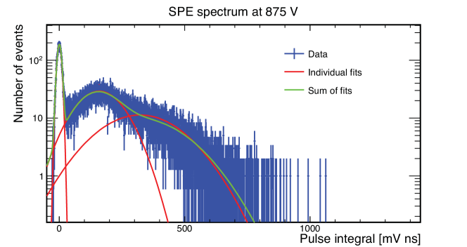
The distribution of the integral of the pulses in mVns is shown in Fig.7. The first peak is the pedestal and is associated to background processes (e.g. leakage current, thermal emission and electronic noise). The second peak comes from single photoelectrons and the third from double photoelectrons. The characteristic Gaussian shape is due to the multiplication process of the dynode chain. The difference between the mean of the single photoelectric peak and the pedestal in pC111 and as obtained from the fit are in mVns. To convert to pC, they must be divided by , divided by the electron charge, , gives the gain of the PMT,
| (2) |
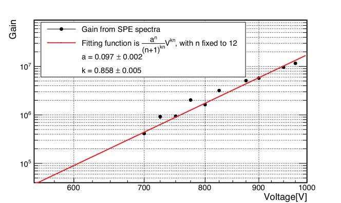
By changing the HV applied to the PMT, the gain as a function of the high-voltage in Fig. 8 is obtained. The points have been fitted with the following formula [35]
| (3) |
where is fixed and corresponds to the number of dynodes (12 for the R11265U PMT series) and can be written as
| (4) |
In Fig. 8 was fixed to 12, with and being the only two free parameters of the fit.
We performed an energy calibration with a standard set of radioactive isotopes (109Cd, 133Ba, 137Cs, 60Co, 57Co, 22Na, 54Mn, 65Zn, 232Th) ranging from (from 109Cd) to (from 208Tl, the last decay of 232Th decay chain). Data have been taken at different high voltage values, namely , , , and . Here we only report the calibration and the corresponding energy resolution at . This will be the operating voltage during the space mission, as it is a good trade-off between performance and low power requirements. The calibration is shown in Fig. 9 and the resolution, which varies from 30% at 30 keV to less than 2% at , is shown in Fig. 10.
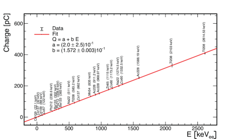
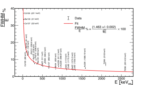
Note that as the calibration uses gamma isotopes, the energy is in units of keVee (“electron equivalent”). For the same amount of energy deposited in the crystal, neutrons and alpha-particles yield less scintillation light, some being lost in non-radiative collisions. Hereby, we express the actual energy deposited by neutrons and alpha-particles in units of keVne (“nuclear equivalent”), with . We plan to measure the linear relation between keVee and keVne in the near future using a neutron source.
5 Detector characterisation as a function of temperature
When orbiting Earth, the RAADSat will be exposed to range of temperatures from about to . For this reason, we tested the basic detector unit between and under vacuum. All the measurements have been performed in the thermal vacuum chamber at the YahSat Space Lab at Masdar Institute (Khalifa University). This chamber works at high vacuum ( mbar) and allows the radiative thermal environment to be controlled within . Three thermosensors (Pt100) were used: one attached to the PMT, one to the crystal and one to the platform where the PMT was seated on the chamber. Temperature readings from the sensors were constantly monitored by a Raspberry PI. Before starting a measurement, we made sure to wait enough time (around one hour) for the temperature to stabilise. The temperatures reported in the following plots refer to the one measured by the thermosensor on the crystal: the temperature of the PMT was found compatible with such temperature within .
Firstly, we performed an energy calibration as a function of temperature using 232Th. The radioactive source was sealed in between two blank flanges and placed in front of the crystal side of the detector in the vacuum chamber. As an example, we show the spectrum taken at in Fig. 11. The peaks have been labelled according to [36].
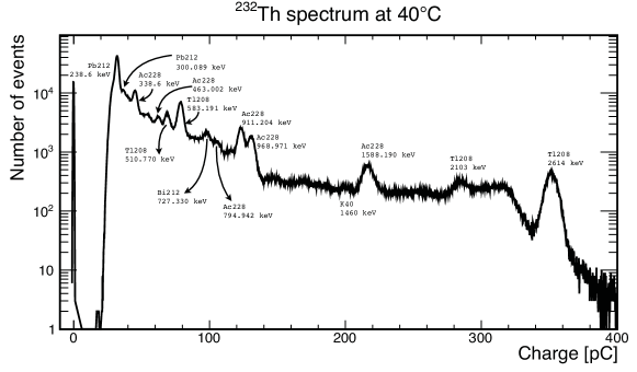
By calibrating the detector at different temperatures using 232Th, we obtain the plot in Fig. 12, where each point represents the mean of the Gaussian fit of the corresponding energy peak in the charge spectrum at a given temperature, and the error bar is the standard deviation coming from the same fit.
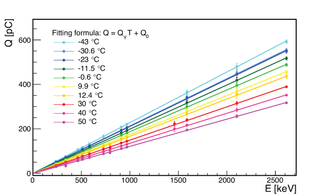
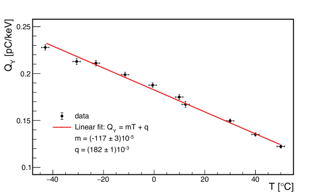
Each data set in Fig.12 is fitted with a linear function222Note that the offset is not fixed to zero, but it turned out to be compatible with zero within uncertainties. to get the charge yield in units of pC/keV as a function of temperature, shown in Fig. 13. Evaluating the function at , the temperature in the lab at NYUAD, gives a charge yield which is compatible within one standard deviation with the charge yield as measured at NYUAD in Fig. 9. The two plots of Fig. 13 and Fig. 9 are obviously key to a proper energy reconstruction of events acquired in orbit.
The dependence of the charge yield on the temperature can in principle be attributed to either the PMT or the crystal. While we do not have sufficient data to support either case, we know from the manufacturer [35] that the temperature coefficient of a bialkali photocathode is ∘C. Using this value, we expect a decrease of charge yield of 37% from C to C, while we observe a decrease of 46%, indicating that most, if not all, of the variation is attributable to the PMT. A dedicated measurement will be needed to precisely disentangle the two contributions.
6 Conclusions
We have fully characterised a prototype scintillation detector for its deployment on a CubeSat mission to study Terrestrial Gamma-ray Flashes. CeBr3(LB) has been chosen as scintillator for its excellent characteristics of speed, resolution, density, and low intrinsic radioactivity. The crystal has been coupled to a lightweight, compact photomultiplier, Hamamatsu R11265U-200, whose factory voltage divider has been replaced to meet the low power constraints of the mission. The unit has been fully calibrated in terms of gain (through single photoelectron measurements), energy, linearity and resolution.
Finally, we have presented the measurement of the temperature coefficient of the detector charge yield. A good detector characterisation as a function of temperature is a key factor for the space mission. In fact, to understand the physics behind TGFs the detector must be able to perform excellent spectroscopy, and it is therefore important to correct the signal amplitudes for temperature variations.
The authors would like to thank M. Marisaldi from University of Bergen for the insightful comments that improved the quality of the work and L. Burderi from University of Cagliari for the fruitful discussions.
References
- [1] E. Kulu, “Nanosatellite & CubeSat Database.” www.nanosats.eu.
- [2] P. Puig-suari, C. Turner and W. Ahlgren, Development of the standard cubesat deployer and a cubesat class picosatellite, vol. 1, pp. 1/347 – 1/353 vol.1, 02, 2001. DOI.
- [3] G. Fishman, P. N Bhat, R. Mallozzi, J. Horack, T. Koshut, C. Kouveliotou et al., Discovery of intense gamma-ray flashes of atmospheric origin, Science (New York, N.Y.) 264 (06, 1994) 1313–1316.
- [4] D. M. Smith et al., Terrestrial Gamma-Ray Flashes Observed up to , Science 307 (2005) 1085–1088.
- [5] M. Marisaldi et al., Detection of terrestrial gamma ray flashes up to 40 mev by the agile satellite, Journal of Geophysical Research 115 (2010) A00E13.
- [6] M. S. Briggs et al., Terrestrial gamma-ray flashes in the fermi era: Improved observations and analysis methods, Journal of Geophysical Research Space Physics 118 (2013) 3805–3830.
- [7] A. Ursi et al., Terrestrial gamma-ray flashes in the BeppoSAX data archive, Journal of Atmospheric and Solar-Terrestrial Physics 156 (Apr., 2017) 50–56.
- [8] D. Smith, J. R. Dwyer, B. J. Hazelton, B. Grefenstette, G. F. M. Martinez-McKinney, Z. Y. Zhang et al., A terrestrial gamma ray flash observed from an aircraft, Journal of Geophysical Research 116 (10, 2011) D20124.
- [9] B. Hare, M. Uman, J. Dwyer, D. Jordan, M. Biggerstaff, J. Caicedo et al., Ground-level observation of a terrestrial gamma ray flash initiated by a triggered lightning: Ground-level observation of a tgf, Journal of Geophysical Research: Atmospheres 121 (06, 2016) .
- [10] R. U. Abbasi, T. Abu-Zayyad, E. Barcikowski, J. Belz, D. R. Bergman, S. Blake et al., Gamma ray showers observed at ground level in coincidence with downward lightning leaders, Journal of Geophysical Research: Atmospheres 123 (05, 2018) 6864–6879.
- [11] M. Marisaldi et al., Enhanced detection of terrestrial gamma-ray flashes by AGILE, Geophysical Research Letters 42 (Nov, 2015) 9481–9487.
- [12] J. R. Dwyer, The relativistic feedback discharge model of terrestrial gamma ray flashes, Journal of Geophysical Research (Space Physics) 117 (02, 2012) 2308–.
- [13] U. S. Inan, S. Reising, G. Fishman and J. Horack, On the association of terrestrial gamma-ray bursts with lightning discharges and sprites, Geophysical Research Letters - GEOPHYS RES LETT 23 (05, 1996) 1017–1020.
- [14] V. Connaughton, M. S. Briggs, S. Xiong, J. R. Dwyer, M. L. Hutchins, J. E. Grove et al., Radio signals from electron beams in terrestrial gamma ray flashes, May, 2013. 10.1029/2012JA018288.
- [15] M. S. Briggs, S. Xiong, V. Connaughton, D. Tierney, G. Fitzpatrick, S. Foley et al., Terrestrial gamma‐ray flashes in the fermi era: Improved observations and analysis methods, Jun, 2013. 10.1002/jgra.50205.
- [16] P. C. T. R. Wilson, The acceleration of -particles in strong electric fields such as those of thunderclouds, Mathematical Proceedings of the Cambridge Philosophical Society 22 (03, 1925) 534 – 538.
- [17] A. Gurevich, G. Milikh and R. Roussel-Dupré, Runaway electron mechanism of air breakdown and preconditioning during a thunderstorm, Physics Letters A 165 (1992) 463 – 468.
- [18] E. R. Williams, Origin and context of c. t. r. wilson’s ideas on electron runaway in thunderclouds, Journal of Geophysical Research 115 (08, 2010) .
- [19] J. R. Dwyer, Z. Saleh, H. K. Rassoul, D. Concha, M. Rahman, V. Cooray et al., A study of X-ray emission from laboratory sparks in air at atmospheric pressure, Journal of Geophysical Research (Atmospheres) 113 (Dec., 2008) D23207.
- [20] J. Dwyer and L. P. Babich, Low-energy electron production by relativistic runaway electron avalanches in air, Journal of Geophysical Research 116 (09, 2011) .
- [21] J. R. Dwyer, The source mechanisms of terrestrial gamma-ray flashes (tgfs), Journal of Geophysical Research 113 (05, 2008) .
- [22] A. B. Skeltved, N. Østgaard, B. Carlson, T. Gjesteland and S. Celestin, Modeling the relativistic runaway electron avalanche and the feedback mechanism with GEANT4, J. Geophys. Res. Space Phys. 119 (2014) 9174, [1605.07771].
- [23] G. D. Moss et al., Monte carlo model for analysis of thermal runaway electrons in streamer tips in transient luminous events and streamer zones of lightning leaders, Journal of Geophysical Research: Space Physics 111 (Feb, 2006) A02307.
- [24] B. E. Carlson, T. Gjesteland and N. Østgaard, Connecting the terrestrial gamma-ray flash source strength and observed fluence distributions: Tgf strength distribution, Journal of Geophysical Research: Space Physics 117 (Jan, 2012) .
- [25] S. Celestin and V. P. Pasko, Energy and fluxes of thermal runaway electrons produced by exponential growth of streamers during the stepping of lightning leaders and in transient luminous events, Journal of Geophysical Research: Space Physics 116 (2011) .
- [26] T. Neubert, N. Østgaard, V. Reglero, E. Blanc, O. Chanrion, C. A. Oxborrow et al., The asim mission on the international space station, Space Science Reviews 215 (Mar, 2019) 26.
- [27] C. N. D. Spatiales, “TARANIS.” https://taranis.cnes.fr/en/TARANIS/index.htm.
- [28] F. Fiore, L. Burderi, T. Di Salvo, M. Feroci, C. Labanti, M. R. Lavagna et al., Hermes: a swarm of nano-satellites for high energy astrophysics and fundamental physics, p. 97, 07, 2018. DOI.
- [29] M. Thiel, W. Doring, V. Dormenev, P. Drexler, R. Novotny, M. Rost et al., High-energy photon detection with lyso crystals, Nuclear Science, IEEE Transactions on 55 (07, 2008) 1425 – 1429.
- [30] J. Chen, L. Zhang and R. yuan Zhu, Large size lso and lyso crystal scintillators for future high-energy physics and nuclear physics experiments, Nuclear Instruments and Methods in Physics Research Section A: Accelerators, Spectrometers, Detectors and Associated Equipment 572 (2007) 218 – 224.
- [31] F. Quarati, P. Dorenbos, J. van der Biezen, A. Owens, M. Selle, L. Parthier et al., Scintillation and detection characteristics of high-sensitivity cebr3 gamma-ray spectrometers, Nuclear Instruments and Methods in Physics Research Section A: Accelerators, Spectrometers, Detectors and Associated Equipment 729 (2013) 596 – 604.
- [32] G. F. Knoll, Radiation detection and measurement; 4th ed. Wiley, New York, NY, 2010.
- [33] Saint-Gobain, “NaI(Tl) and Polyscin NaI(Tl) Sodium Iodide.” https://www.crystals.saint-gobain.com/products/nai-sodium-iodide.
- [34] C. Lois, P. Aguiar, B. Couce and A. Iglesias, Characterization of low energy lu background on continuous lyso blocks, IEEE Nuclear Science Symposuim & Medical Imaging Conference, (2010) 1 – 3.
- [35] H. Photonics, Photomultiplier tubes, Basics and applications. Hamamatsu Photonics, 3 ed., 2007.
- [36] Library of Recommended Actinide Decay Data, 2011. Non-serial Publications. INTERNATIONAL ATOMIC ENERGY AGENCY, Vienna, 2013.