Controlling the quantum spin Hall edge states in two-dimensional transition metal dichalcogenides
Abstract
Two-dimensional transition metal dichalcogenides (TMDs) of Mo and W in their 1T’ crystalline phase host the quantum spin Hall (QSH) insulator phase. We address the electronic properties of the QSH edge states by means of first-principles calculations performed on realistic models of edge terminations of different stoichiometries. The QSH edge states show a tendency to have complex band dispersions and coexist with topologically trivial edge states. We nevertheless identify two stable edge terminations that allow isolating a pair of helical edge states within the band gap of TMDs, with monolayer 1T’- being the most promising material. We also characterize the finite-size effects in the electronic structure of 1T’- nanoribbons. Our results provide a guidance to the experimental studies and possible practical applications of QSH edge states in monolayer 1T’-TMDs.
Two-dimensional transition metal dichalcogenides (2D TMDs) of chemical composition , where is a transition metal element and = S, Se or Te, is a broad family of emerging 2D materials that attracts ever increasing interest Wang et al. (2012); Chhowalla et al. (2013); Manzeli et al. (2017). Among them, group VI TMDs ( = Mo, W) in their 2H crystalline phase continue receiving special attention due to their semiconducting band gaps that span a broad interval of energies Mak et al. (2010); Splendiani et al. (2010), which makes them suitable for diverse applications that include electronics and optoelectronics Radisavljevic et al. (2011), photovoltaics Bernardi et al. (2013); Ugeda et al. (2014) and sensors devices Perkins et al. (2013). Strong spin-orbit interactions in these materials Zhu et al. (2011) results in an intrinsic spin-valley coupling Xiao et al. (2012) responsible for novel transport properties Habe and Koshino (2015); Pulkin and Yazyev (2016), the exotic Ising superconductor phase Lu et al. (2015), and more. While the 2H phase is the thermodynamically stable polymorph for all group VI TMDs except WTe2, the metastable 1T phase has also been widely documented Voiry et al. (2015). The 1T phase is prone to lattice instabilities Duerloo et al. (2014); Pasquier and Yazyev giving rise to the so-called 1T’ phase that features dimer-chain distortions observed in experiments Chou et al. (2015); Gao et al. (2015); Keum et al. (2015); Cho et al. (2015); Jia et al. (2017); Peng et al. (2017). The structures of these polymorphs of 2D TMDs are summarized in Figure 1a.
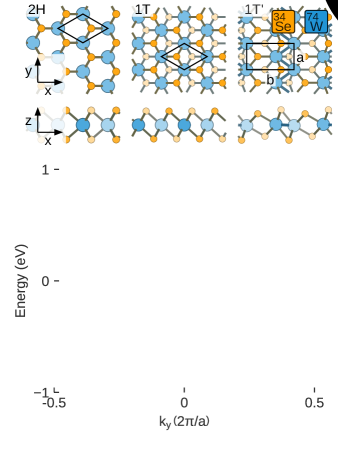
The 1T’ crystalline polymorph of group VI monolayer TMD materials was theoretically predicted to realize the quantum spin Hall (QSH) insulator phase Qian et al. (2014). This topological electronic phase is due to the combination of band inversion and spin-orbit interactions that open few tens millielectronvolt band gaps Kane and Mele (2005); Choe et al. (2016). A representative electronic band structure of monolayer 1T’- is shown in Figure 1b. The predicted QSH insulator phase soon received experimental confirmation in monolayer 1T’- using both spectroscopic techniques and transport measurements Tang et al. (2017); Fei et al. (2017). More recently, the same topological phase was observed in metastable monolayer 1T’- further extending this family of 2D topological insulators Chen et al. (2018); Ugeda et al. (2018).
The most important consequence of the QSH insulator phase in material’s bulk is the presence of helical edge states at its boundaries. The properties of the topological edge states in 2D TMDs are extensively discussed Qian et al. (2014); Tang et al. (2017); Ugeda et al. (2018); Wu et al. (2018); Jelver et al. (2019) in the context of unconventional electronics and quantum computing due to their unique properties: formation of exotic quasiparticles, spin-momentum locking, protection against backscattering, to name just a few Kitaev (2009); Hasan and Kane (2010); Qi and Zhang (2011). While the existence of these topological edge states is guaranteed by bulk topology, the details of their band dispersion and spin texture would depend on the local structure of the edges, such as the crystallographic orientation, chemical composition and terminationWang et al. (2014). More importantly, the simultaneous presence of undesired topologically trivial edge states is not guaranteed by any existing argument. Thus, establishing the relations between the structure of the edges and the properties of QSH edge states is of crucial importance for advancing the fundamental physics and realizing technological applications of these topological phases.
In this Letter, we address the properties of the quantum spin Hall edge states in monolayer 1T’-phase transition metal dichalcogenides from first principles. We consider realistic edge terminations of different chemical composition identifying stable configurations. Our non-equilibrium Green’s function (NEGF) calculations reveal predominantly complex dispersions of the QSH edge states coexisting with topologically trivial edge states. Two edge terminations, however, were shown to host an isolated pair of helical states. We also address finite-size effects in the electronic structure of 1T’- nanoribbon models providing further guidance to the experimental studies of these novel topological states.
Our first-principles electronic structure calculations have been performed using the OpenMX software package within the framework of density functional theory (DFT) and localized pseudoatomic orbital basis sets Ozaki (2003); Ozaki and Kino (2004). The basis set used in our work contains 25 basis functions per transition metal atom (s2p2d2f1) and 14 basis functions per chalcogen atom (s3p3d1), which is sufficient for accurate description of the electronic structure. The calculations have been performed using the PBE exchange-correlation functional Perdew et al. (1996) and taking into account the spin-orbit interaction. The relaxed atomic structures of the edges were obtained in the nanoribbon geometry of width up to 5.5 nm with two equivalent edges. The electronic structure of the edges was then addressed using semi-infinite models combined with the tight-binding Kohn-Sham Hamiltonian and overlap matrices obtained from DFT calculations. The local density of electronic states was calculated using the surface Green’s function approach.
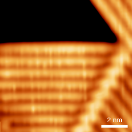
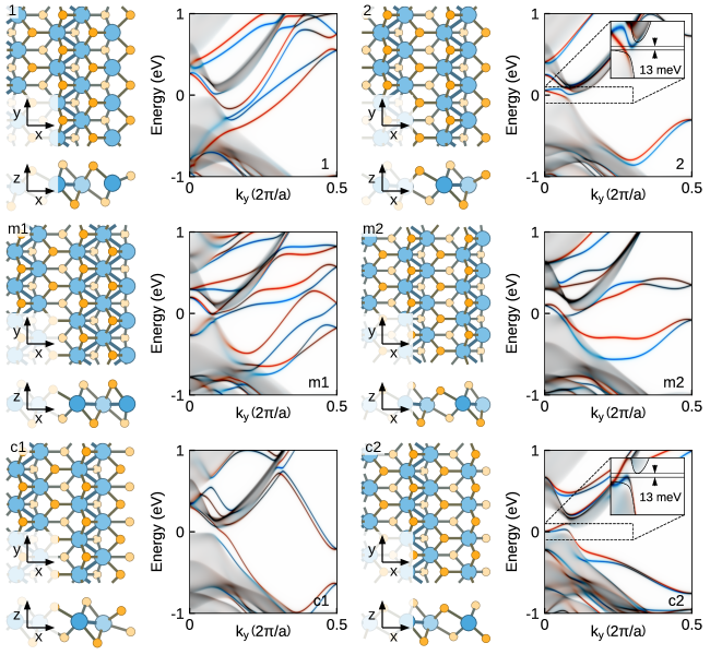
Even though our work addresses all six TMDs involving group VI transition metals, we will focus our discussion on as a representative example for the reasons explained below. Fig. 1d shows the electronic band structure of monolayer 1T’-. The calculated band gap of 29 meV agrees well with previous studies performed at the DFT level Qian et al. (2014); Pulkin and Yazyev (2017), while the evident flattening of the valence band is indicative of band inversion responsible for the QSH phase. The presence of the topological phase gives rise to the helical states localized at the interface with a topologically trivial medium Kane and Mele (2005), with the simplest example of such an interface being the edge. The edges can be characterized by various crystallographic orientations and terminations, with the ones corresponding to the lowest formation energies being thermodynamically preferred. The crystallographic orientation of the edges is defined by the periodicity vector , where , are the lattice vectors of the 1T’-TMD monolayer, see Fig. 1(a). Below, we will limit our consideration to the shortest possible that corresponds to the “zigzag” direction of the underlying honeycomb lattice. Such edges are prevalent in the CVD-grown 2H-phase TMDs van der Zande et al. (2013); Zhou et al. (2013); Dumcenco et al. (2015) as well as in monolayer 1T’- Peng et al. (2017). More recently, the tendency to form well-ordered edges was also observed in 1T’- by means scanning tunneling miscroscopyPedramrazi et al. (2019). Figure 2 reproduces one of experimental images of such edges coexisting with a 1T’-1T’ domain boundary. The dimer rows appear to be aligned parallel to the edges, and we will reproduce this feature in our models. We consider six different terminations of the edges shown in Fig. 3, which can be divided into three groups (rows in Fig. 3) according to the local chemical composition – stoichiometric (1 and 2), metal-rich (m1 and m2) and chalcogen-rich (c1 and c2). The two configurations in each pair differ by the position of the dimer chains relative to the edge. Since TMDs have binary chemical composition, the formation energies of the edges depend on the chemical potentials of the elements. The former is defined per unit length as
| (1) |
where is the total energy of a nanoribbon model with two identical edges, and are the numbers of W and Se atoms in the model, respectively, and are the corresponding chemical potentials and is the lattice constant in Fig. 1. The chemical potentials of the two elements are subject to the bulk-phase energy constraint
| (2) |
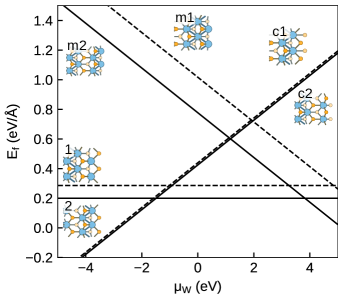
The formation energies of terminations 1, m1 and c1 in Fig. 3 differ from those of terminations 2, m2 and c2, respectively, by a constant since in each pair of models the edges have the same chemical composition. Figure 4 shows the formation energies all six edge configurations for monolayer 1T’- as a function of with that corresponds to bulk bcc tungsten. Three different terminations (2, m2 and c2) can be identified as the most stable within distinct ranges of the chemical potential. Other monolayer 1T’-TMDs show a similar behavior, in particular, the metal-rich structure m1 is always energetically unfavorable suggesting that the unbound chain of metal atoms at the edge has a considerable energy overhead. The corresponding plots of formation energies as a function of the chemical potential of metal are presented in the Supplementary Material document. We would also like to point out that all investigated edge terminations for all six TMDs do not show any local magnetic moments at the edge, which is of crucial importance for exploiting the topological protection of the QSH edge states. This result contrasts to a recent investigation that finds magnetic edge configurations for monolayer 1T’- edges Jelver et al. (2019).
The electronic structure of the considered six configurations is addressed by plotting the momentum- and spin-resolved local density of states at the edge, shown in half of the Brillouin zone in Fig. 3. Bulk electronic states of monolayer 1T’-TMDs are spin-degenerate due to the presence of time-reversal and inversion symmetries. However, inversion symmetry is broken at the edges, hence spin-degeneracy of the edge states is expected to be lifted. This allows to unambiguously distinguish bulk and edge states in the discussed local density of states plots. Bulk states appear as gray areas that correspond to the projections of the 2D bulk band structure onto the momentum parallel to the edge. The shape of these areas does not depend on the local atomic structure of the edges. In contrast, edge states are spin-polarized (in Fig. 3 color-coding reflects the expectation value of the operator, with red and blue corresponding to spin-up and spin-down channels, respectively) and appear as band features that vary strongly upon changing the edge termination. The spin-polarized bands cross the Fermi level an odd number of times as expected for the topologically non-trivial QSH phase in monolayer 1T’-. In general, the dispersion of edge states in monolayer 1T’- and other 1T’-TMDs is very complex as compared to the idealized picture of two linearly dispersing bands forming a single crossing. The number of localized modes inside the band gap varies strongly and may be as large as 7 per spin (terminations 1 and m1). These bands can be viewed as the topological QSH edge states combined with the topologically trivial edge states that show a typical Rashba-like dispersion Bychkov and Rashba (1984). Interestingly, the out-of-plane spin-polarization of the edge bands is not always preserved across the entire Brillouin zone. For example, in the case configuration m2 two edge states form an avoided crossing due to the spin-orbit coupling at which spin mixing takes place and hence the spinor wavefunctions are no longer eigenstates of the spin operator.
The topological protection of ballistic transport of charge carriers refers to a process in which charge carriers are supported by one of the two helical edge modes of the QSH insulator without backscattering. This fundamental property of the topological edge states is interesting from the point of view of exploring novel physical phenomena as well as technological applications. One often quoted idea is the use of the QSH edge channels as interconnect in nanoelectronic devices that operate in dissipationless ballistic transport regime. These applications, however, depend critically on the ability to isolate the QSH edge states from bulk states as well as topologically trivial edge states within the gap that may enable scattering processes. We therefore focus on identifying the combination of edge termination and material composition that results in the presence of a single pair of QSH edge states within the gap and not accompanied by additional topologically trivial bands. According to our calculations, this condition is satisfied only for edge terminations 2 and c2 in monolayer 1T’-. The dispersion of edge-state bands in other studied TMDs is qualitatively similar (see Supplementary Material), but 1T’- shows the broadest energy ranges in which a single pair of QSH helical edge states is isolated. Insets in Fig. 3 show that in both cases the QSH edge states are isolated within the energy range of 13 meV inside the 29 meV band gap of monolayer 1T’-. In the case of stoichiometric termination 2 this energy window is pinned to the valence band maximum, while in the case of chalcogen-rich termination c2 it is located at the conduction band minimum of monolayer 1T’-. We thus conclude that this particular material and these two edge terminations present the most favorable combination for addressing the QSH physics and potential technological applications among the 2D TMD topological insulators. For the same reason, our discussion focuses on this representative of the 1T’-phase monolayer TMD family of materials.
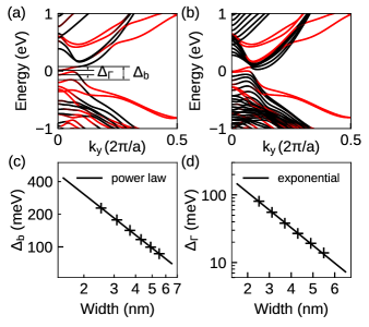
We will now address the finite-size effects on the bulk and edge states of monolayer 1T’- by considering nanoribbons of different width. The interplay of the following two effects is expected to govern the electronic structure of nanoribbons upon decreasing width: (i) increase of the bulk band gap due to the quantum confinement effects, and (ii) hybridization of the edge states localized at the opposite edges due to a finite wavefunction overlap, which results in a gap opening at the point where the edge-state bands cross Huang et al. (2013) (see Fig. 5a for definitions). To understand how these two quantities depend on the nanoribbon width we performed DFT calculations of monolayer 1T’- nanoribbons up to width nm assuming the c2 termination of both edges. For each nanoribbon model, we calculated the band structure in the 1D Brillouin zone and analyzed the spatial distribution of the Bloch states. This allowed us to assign the states either bulk or edge character, shown in black and red in Figs. 5a,b for two representative nanoribbons of 2.5 nm and 5.5 nm width, respectively. The dispersion of edge states clearly resembles the results of calculations performed on semi-infinite models (Fig. 3) with the bulk-like states forming a series of sub-bands due to the quantum confinement. The bulk band gap was calculated by considering only those states having a significant orbital contribution originating from the nanoribbon bulk. Figs. 5c,d summarize the results for both and as a function of nanoribbon width . The effect of quantum confinement on the bulk band gap can be understood as a result of the quantization of the Bloch wavevector perpendicular to the nanoribbon edge. The band structure of 1D nanoribbons is composed of the states of the 2D band structure of bulk material with
| (3) |
where is the nanoribbon width given in terms of the corresponding lattice constant , and is a positive integer. The band gap in monolayer 1T’- occurs between the band extrema located at , which are never satisfied by the above condition. Thus, the size of the bulk band gap of nanoribbons is expected to be always larger than the gap of the parent bulk material. In the limit of infinite width the nanoribbon gap converges to the bulk band gap. Correspondingly, the values of shown in Fig. 5c can be described by a power law that depends the particularities of the dispersion of bulk bands close to the band gap edges. Numerical fit of the results to with being fixed to the bulk band gap of monolayer 1T’- yields (line in Fig. 5c). The obtained exponent differs significantly from expected for the ideal quadratic bands. We ascribe this difference to the peculiar shape of bulk bands strongly affected by band inversion in this material.
Unlike governed by the bulk properties, the gap opening at the point is rather defined by the exponential decay of edge states. The values calculated for monolayer 1T’- nanoribbons shown in Fig. 5d can be accurately fitted by
| (4) |
with eV and a characteristic decay length of edge states nm. This relatively fast exponential decay combined with a slower polynomial decay of the bulk band gap suggests a regime, in which quantum confinement can be used to enhance the bulk band gap of the topological insulator phase with no significant hybridization of the edge states.
To summarize, our work reveals that the dispersion of topological QSH edge states and the presence of trivial edge states within the band gap of monolayer 1T’-phase transition metal dichalcogenides depends strongly on the stoichiometry and termination of the edges. We identify edge terminations that are stable and allow isolating a pair of helical edge states within the band gap. Focusing on monolayer 1T’- as a representative example we address also the finite-size effects in the electronic structure, thus providing a guidance to the experimental studies and possible practical applications of QSH edge states in monolayer 1T’-TMDs.
Acknowledgments. We acknowledge support by the ERC Starting grant “TopoMat” (Grant No. 306504) and NCCR Marvel. Author A.P. thanks Swiss NSF for the support provided through Early Postdoc.Mobility program (project P2ELP2_175281). First-principles calculations were performed at the Swiss National Supercomputing Centre (CSCS) under project s832 and the facilities of Scientific IT and Application Support Center of EPFL. We thank C. Herbig, Z. Pedramrazi and M. F. Crommie for providing the STM image reproduced in Figure 2.
References
- Wang et al. (2012) Q. H. Wang, K. Kalantar-Zadeh, A. Kis, J. N. Coleman, and M. S. Strano, Nature Nanotechnology 7, 699 (2012).
- Chhowalla et al. (2013) M. Chhowalla, H. S. Shin, G. Eda, L.-J. Li, K. P. Loh, and H. Zhang, Nat. Chem. 5, 263 (2013).
- Manzeli et al. (2017) S. Manzeli, D. Ovchinnikov, D. Pasquier, O. V. Yazyev, and A. Kis, Nat. Rev. Mater. 2, 17033 (2017).
- Mak et al. (2010) K. F. Mak, C. Lee, J. Hone, J. Shan, and T. F. Heinz, Physical Review Letters 105, 136805 (2010).
- Splendiani et al. (2010) A. Splendiani, L. Sun, Y. Zhang, T. Li, J. Kim, C.-Y. Chim, G. Galli, and F. Wang, Nano Letters 10, 1271 (2010).
- Radisavljevic et al. (2011) B. Radisavljevic, A. Radenovic, J. Brivio, V. Giacometti, and A. Kis, Nature Nanotechnology 6, 147 (2011).
- Bernardi et al. (2013) M. Bernardi, M. Palummo, and J. C. Grossman, Nano Letters 13, 3664 (2013).
- Ugeda et al. (2014) M. M. Ugeda, A. J. Bradley, S.-F. Shi, F. H. da Jornada, Y. Zhang, D. Y. Qiu, W. Ruan, S.-K. Mo, Z. Hussain, Z.-X. Shen, F. Wang, S. G. Louie, and M. F. Crommie, Nature Materials 13, 1091 (2014).
- Perkins et al. (2013) F. K. Perkins, A. L. Friedman, E. Cobas, P. M. Campbell, G. G. Jernigan, and B. T. Jonker, Nano Letters 13, 668 (2013).
- Zhu et al. (2011) Z. Y. Zhu, Y. C. Cheng, and U. Schwingenschlögl, Phys. Rev. B 84, 153402 (2011).
- Xiao et al. (2012) D. Xiao, G.-B. Liu, W. Feng, X. Xu, and W. Yao, Physical Review Letters 108, 196802 (2012).
- Habe and Koshino (2015) T. Habe and M. Koshino, Phys. Rev. B 91, 201407 (2015).
- Pulkin and Yazyev (2016) A. Pulkin and O. V. Yazyev, Phys. Rev. B 93, 041419 (2016).
- Lu et al. (2015) J. M. Lu, O. Zheliuk, I. Leermakers, N. F. Q. Yuan, U. Zeitler, K. T. Law, and J. T. Ye, Science 350, 1353 (2015).
- Voiry et al. (2015) D. Voiry, A. Mohite, and M. Chhowalla, Chem. Soc. Rev. 44, 2702 (2015).
- Duerloo et al. (2014) K.-A. N. Duerloo, Y. Li, and E. J. Reed, Nat. Commun. 5 (2014).
- (17) D. Pasquier and O. V. Yazyev, arXiv:1901.10588 .
- Chou et al. (2015) S. S. Chou, Y.-K. Huang, J. Kim, B. Kaehr, B. M. Foley, P. Lu, C. Dykstra, P. E. Hopkins, C. J. Brinker, J. Huang, and V. P. Dravid, Journal of the American Chemical Society 137, 1742 (2015).
- Gao et al. (2015) P. Gao, L. Wang, Y. Zhang, Y. Huang, and K. Liu, ACS Nano 9, 11296 (2015).
- Keum et al. (2015) D. H. Keum, S. Cho, J. H. Kim, D.-H. Choe, H.-J. Sung, M. Kan, H. Kang, J.-Y. Hwang, S. W. Kim, H. Yang, K. J. Chang, and Y. H. Lee, Nature Physics 11, 482 (2015).
- Cho et al. (2015) S. Cho, S. Kim, J. H. Kim, J. Zhao, J. Seok, D. H. Keum, J. Baik, D.-H. Choe, K. J. Chang, K. Suenaga, S. W. Kim, Y. H. Lee, and H. Yang, Science 349, 625 (2015).
- Jia et al. (2017) Z.-Y. Jia, Y.-H. Song, X.-B. Li, K. Ran, P. Lu, X.-Y. Zhu, Z.-Q. Shi, J. Sun, J. Wen, D. Xing, and S.-C. Li, Physical Review B 96, 041108 (2017).
- Peng et al. (2017) L. Peng, Y. Yuan, G. Li, X. Yang, J.-J. Xian, C.-J. Yi, Y.-G. Shi, and Y.-S. Fu, Nature Communications 8, 659 (2017).
- Qian et al. (2014) X. Qian, J. Liu, L. Fu, and J. Li, Science 346, 1344 (2014).
- Kane and Mele (2005) C. L. Kane and E. J. Mele, Physical Review Letters 95, 146802 (2005).
- Choe et al. (2016) D.-H. Choe, H.-J. Sung, and K. J. Chang, Physical Review B 93, 125109 (2016).
- Tang et al. (2017) S. Tang, C. Zhang, D. Wong, Z. Pedramrazi, H.-Z. Tsai, C. Jia, B. Moritz, M. Claassen, H. Ryu, S. Kahn, J. Jiang, H. Yan, M. Hashimoto, D. Lu, R. G. Moore, C.-C. Hwang, C. Hwang, Z. Hussain, Y. Chen, M. M. Ugeda, Z. Liu, X. Xie, T. P. Devereaux, M. F. Crommie, S.-K. Mo, and Z.-X. Shen, Nature Physics 13, 683 (2017).
- Fei et al. (2017) Z. Fei, T. Palomaki, S. Wu, W. Zhao, X. Cai, B. Sun, P. Nguyen, J. Finney, X. Xu, and D. H. Cobden, Nat. Phys. 13, 677 (2017).
- Chen et al. (2018) P. Chen, W. W. Pai, Y. H. Chan, W. L. Sun, C. Z. Xu, D. S. Lin, M. Y. Chou, A. V. Fedorov, and T. C. Chiang, Nat. Commun. 9, 2003 (2018).
- Ugeda et al. (2018) M. M. Ugeda, A. Pulkin, S. Tang, H. Ryu, Q. Wu, Y. Zhang, D. Wong, Z. Pedramrazi, A. Martín-Recio, Y. Chen, F. Wang, Z.-X. Shen, S.-K. Mo, O. V. Yazyev, and M. F. Crommie, Nature Communications 9, 3401 (2018).
- Wu et al. (2018) S. Wu, V. Fatemi, Q. D. Gibson, K. Watanabe, T. Taniguchi, R. J. Cava, and P. Jarillo-Herrero, Science 359, 76 (2018).
- Jelver et al. (2019) L. Jelver, D. Stradi, K. Stokbro, T. Olsen, and K. W. Jacobsen, Physical Review B 99, 155420 (2019).
- Kitaev (2009) A. Kitaev, in AIP Conference Proceedings, Vol. 1134 (AIP Publishing, 2009) pp. 22–30.
- Hasan and Kane (2010) M. Z. Hasan and C. L. Kane, Reviews of Modern Physics 82, 3045 (2010).
- Qi and Zhang (2011) X.-L. Qi and S.-C. Zhang, Reviews of Modern Physics 83, 1057 (2011).
- Wang et al. (2014) Z. F. Wang, L. Chen, and F. Liu, Nano Letters 14, 2879 (2014).
- Ozaki (2003) T. Ozaki, Physical Review B 67, 155108 (2003).
- Ozaki and Kino (2004) T. Ozaki and H. Kino, Physical Review B 69, 195113 (2004).
- Perdew et al. (1996) J. P. Perdew, K. Burke, and M. Ernzerhof, Physical Review Letters 77, 3865 (1996).
- Pedramrazi et al. (2019) Z. Pedramrazi, C. Herbig, A. Pulkin, S. Tang, M. Phillips, D. Wong, H. Ryu, M. Pizzochero, Y. Chen, E. J. Mele, F. Wang, Z.-X. Shen, S.-K. Mo, O. V. Yazyev, and M. F. Crommie, Nano Letters (2019), 10.1021/acs.nanolett.9b02157.
- Pulkin and Yazyev (2017) A. Pulkin and O. V. Yazyev, Journal of Electron Spectroscopy and Related Phenomena 219, 72 (2017).
- van der Zande et al. (2013) A. M. van der Zande, P. Y. Huang, D. A. Chenet, T. C. Berkelbach, Y. You, G.-H. Lee, T. F. Heinz, D. R. Reichman, D. A. Muller, and J. C. Hone, Nature Materials 12, 554 (2013).
- Zhou et al. (2013) W. Zhou, X. Zou, S. Najmaei, Z. Liu, Y. Shi, J. Kong, J. Lou, P. M. Ajayan, B. I. Yakobson, and J.-C. Idrobo, Nano Letters 13, 2615 (2013).
- Dumcenco et al. (2015) D. Dumcenco, D. Ovchinnikov, K. Marinov, P. Lazić, M. Gibertini, N. Marzari, O. L. Sanchez, Y.-C. Kung, D. Krasnozhon, M.-W. Chen, S. Bertolazzi, P. Gillet, A. Fontcuberta i Morral, A. Radenovic, and A. Kis, ACS Nano 9, 4611 (2015).
- Bychkov and Rashba (1984) Y. A. Bychkov and E. I. Rashba, JETP Lett. 39, 78 (1984).
- Huang et al. (2013) L. F. Huang, G. R. Zhang, X. H. Zheng, P. L. Gong, T. F. Cao, and Z. Zeng, Journal of Physics: Condensed Matter 25, 055304 (2013).