e-mail paschen@ifp.tuwien.ac.at, Phone: +43-1-58801-13716, Fax: +43-1-58801-13899
2 Center for Micro- and Nanostructures, TU Wien, Floragasse 7, A-1040 Vienna, Austria
3 Faculty of Materials Science and Engineering, K. N. Toosi University of Technology, Tehran, Iran
4 Universitäre Service-Einrichtung für Transmissions-Elektronenmikroskopie, TU Wien, Wiedner Hauptstr. 8-10, 1040 Vienna, Austria
5 Institute of Physical Chemistry, University of Vienna, Währinger Strasse 42, 1090 Vienna, Austria
6 Laboratory for Solid State Chemistry and Catalysis, EMPA, Überlandstrasse 129, 8600 Dübendorf, Switzerland
7 Institut für Materialwissenschaft, Universität Stuttgart, Heisenbergstr. 3, 70569 Stuttgart, Germany
XXXX
Nanostructured clathrates and clathrate-based nanocomposites
Abstract
\abstcolIntermetallic clathrates are candidate materials for thermoelectric applications above room temperature. Here we explore whether their intrinsically low lattice thermal conductivities can be further reduced by nanostructuring and whether this can further enhance their thermoelectric performance.As bulk nanostructuring routes we studied melt spinning and ball milling. To optimize the compaction process and/or stabilize the nanostructure we varied the process parameters, used additives, and studied clathrate-based composites. Initial results on clathate nanowires as simpler model nanostructures are also presented.
keywords:
clathrates, hot pressing, nanostructuring, melt spinning, thermoelectric and transport measurements, thermoelectric materials1 Introduction
Nanostructuring has in recent years been one of the most extensively explored optimization strategies for thermoelectric materials. It has been shown to enhance the thermoelectric efficiency of traditional thermoelectric materials both for model systems [1, 2] and for bulk materials [3, 4, 5, 6, 7]. On intermetallic clathrates comparatively little has been done. These cage-like materials have intrinsically low lattice thermal conductivities and thus the nanostructuring route, which aims primarily at reducing the lattice thermal conductivity without degrading the electronic properties to much, is less obvious to succeed. Here we present such a study. We have investigated melt spinning as bottom-up and ball milling as top-down technique for the production of nanostructured bulk clathrates. To stabilize the nanostructures we have also explored clathrate-based nanocomposites. Finally we present our nanowire measurement setup to study model nanostructures.
2 Melt spinning
Melt spinning comprises injecting a metal melt onto the surface of a rapidly rotating copper wheel, which results in very high cooling rates of the order 105 - 106 K/s. This process was originally developed for the preparation of amorphous materials and has been the main technique for the production of metallic glasses. Metal alloys with lower glass forming ability usually form nanometer-sized polycrystalline materials. The advantage of the technique for preparation of nanocrystalline materials is its simplicity and short process duration resulting in a lower probability of oxidation. Moreover, clathrate phases typically have broader composition/homogeneity ranges which allows to optimize their thermoelectric properties in a broader range [8, 9]. Melt spinning has shown to be an appropriate technique for nanostructuring of some thermoelectric materials [10, 11, 12]. In particular, the technique was used to prepare Bi2Te3 with nano-layered microstructure with layer thicknesses of 10 - 40 nm [13].
However, our first experiments on the melt spinning of clathrates yielded samples with grain sizes of at least 1 m [8, 9, 15]. This might point to a very high crystallite growth rate of the clathrate phase. For this reason, the formation of foreign phases appeared to be kinetically suppressed. On the one hand this is a great advantage for producing bulk clathrates since the typically needed long-term annealing to remove foreign phases can be omitted. On the other hand this hampers the direct application of melt spinning for the production of nanostructured clathrates. Thus, a profound investigation of the applicability of melt spinning to nanostructure clathrates appeared necessary to understand the specifics of clathrates in rapid cooling processes.
Clathrates have very high crystal as opposed to glass forming ability. Thus all measures which usually lead to glass formation should reduce the clathrate grain size. We describe two approaches. Firstly, we adjusted the parameters of the melt spinning process. We varied the temperature of the melt (melt overheating) and the cooling rate (Sect. 2.2). Secondly, we studied the effect of the melt composition on the grain size (Sect. 2.3).
2.1 Experimental details
The polycrystalline starting materials were prepared by melting elementary metals in a water cooled copper boat in argon atmosphere using high-frequency heating (purity of metals better than 99.95%). At least three re-meltings were done for sample homogenization. For melt spinning the inductively heated melt was sprayed from a fused silica nozzle onto the surface of a quickly rotating (600 - 3000 revolutions per minute, rpm) copper wheel, with a diameter of 30 cm. This method provided a cooling rate of about 105 - 106 K/s. Both the slow and rapid crystallizations were performed in argon atmosphere.
Scanning electron microscopy (SEM) and high-resolution transmission electron microscopy (TEM) investigations were performed on Philips XL30 ESEM (with an EDAX New XL-30 135-10 UTW+ detector) and FEI TECNAI F20 microscopes, respectively. The data reduction of the spectra and quantitative analyses were done by the EDX Control Software (from EDAX Inc.). X-ray powder diffraction (XRD) data were collected using a Siemens D5000 diffractometer with Cu-Kα1,2 radiation. Electrical resistivity and Hall effect measurements were done in a Physical Property Measurement System (PPMS) of Quantum Design. The typical sample size for electrical resistivity measurements was mm3.
To measure the thermal conductivity, we used either thermal diffusivity measurements (Flash technique) or the 3 method. The latter is an ac technique which heats the sample locally and thus reduces errors caused by radiation at room temperature and below to a negligibly small level [16]. A narrow metal line (20 m wide and 1 mm long) serves as both the heater and the thermometer. To avoid electrical contact between heater and sample the polished sample surfaces were covered with a thin layer of SiO2 by chemical vapor deposition. The heater structures were made by standard optical lithography techniques using a Karl Suess MJB4 mask aligner. Sputtering of a 4 nm thick titanium sticking layer and the 64 nm gold film was done in an Ardenne LS 320 S sputter system. The metal line was heated by an oscillating current at a circular frequency , which thus leads to a 2 temperature oscillation of both the heater and the sample. Due to the linear temperature dependence of the metallic heater, the 2 temperature oscillation translates to a 3 voltage oscillation, which is detected using a lock-in amplifier (7265, Signal Recovery). Prior to the thermal 3 voltage detection, the first harmonic and all related higher harmonics are subtracted from the signal using an active filter design based on the technique suggested by Cahill et al. [17, 16]. More details on our 3 measurements are given in Ref. [18].
The phonon contribution was evaluated by subtracting the electronic part from the total thermal conductivity , using the Wiedemann-Franz law with = 2.44 x 10⁻⁸ V2K-2.
2.2 Process parameters for melt spinning of clathrates
The transition metal clathrate phase Ba8AuxSi46-x was chosen for the melt spinning experiments because of its rather wide homogeneity range (about ) [19, 20], which lowers the risk for foreign phases formation. Also, as a rule, a difference in atomic size % strengthens the glass forming ability of metallic phases. The atomic size difference of Au and Si is just 10 %.
We used as starting Au content. It is interesting to note that it was a Au-Si alloy that was first obtained as metal glass by rapid quenching [21]. Three different melt spinning experiments were performed (Table 1). Samples 1 and 2 were quenched with a wheel rotation speed of 1500 rpm from two different melt temperatures, 1300∘C (just above the melting point of 1260∘C) and 1600∘C, respectively. Sample 3 was quenched at a higher rotation speed of 2500 rpm from 1300∘C. Usually melt spinning is carried out in inert gas atmosphere. However, very fast wheel rotation leads to a gas turbulence near the wheel surface, which destroys the melt jet and leads to the formation of small droplets before the material reaches the cooling surface. Therefore sample 3 was quenched in vacuum.
| Quenching | Wheel rotation | Atmosphere | |
|---|---|---|---|
| temperature (∘C) | speed (rpm) | ||
| sample 1 | 1300 | 1500 | 300 mbar Ar |
| sample 2 | 1600 | 1500 | 300 mbar Ar |
| sample 3 | 1300 | 2500 | Vacuum |
The SEM investigation of the obtained samples revealed micrometer or submicrometer sized clathrate grains. Neither higher rotating (cooling) rate (2500 vs 1500 rpm) nor higher starting melt temperature (1600 vs 1300∘C) led to a reduction of the grain size. A detailed microscopy investigation of the obtained materials is described in Sect. 2.4.
2.3 Composition effect in meltspun Ba8Ga16Ge30 clathrate
A well-known strategy to promote glass formation is to increase the number of constituting elements, preferably of considerably different atomic size [22]. Here we used the clathrate Ba8Ga16Ge30 as starting material and partially substitute all three elements (Ba, Ga, Ge) with isovalent elements to obtain a clathrate phase (Ba, Sr, Eu)8(Ga, Al, In)x(Ge, Si, Sn)46-x. The In and Sn substitution would be especially important because of the much larger atomic radii (1.66 and 1.62, respectively) compared to the ones of Ga, Al, Ge, and Si (atomic radii of 1.32 - 1.43 Å). Contrary to the case of an amorphous final product the element ratio in the quenched clathrate melt cannot be varied arbitrarily. The melt composition for quenching should correspond to a stable crystalline clathrate phase as otherwise foreign phases would form during crystallization.
In the search for a stable clathrate phase the nominal composition (Ba1/3Sr1/3Eu1/3)8(Al6Ga6In4)(Si5Ge15Sn10) was prepared by melting the elements followed by fast cooling in a cold boat. The sample was a mixture of a number of phases, whose individual compositions were investigated by SEM/EDX. Among them two phases had element ratios close to the prototypal MAB phase. XRD confirmed the presence of at least two clathrate phases. According to their measured compositions (Ba6Sr1.4Eu0.9)(Ga6.6Al7.7In0.3)(Ge16.8Si13.5Sn0.5) and (Ba5.3Sr2Eu1.0)(Ga9.9Al4.8In0.3)(Ge25Si4.9Sn0.5) the phases were prepared in pure form (hereafter referred to as sample A and sample B, respectively). From the small contents (0.6 - 1.0 at.% In and Sn) we see that the large sized atoms In and Sn are reluctant to enter the clathrate structure.
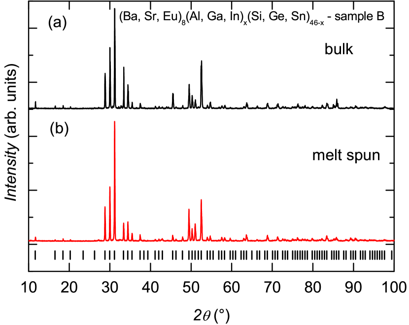
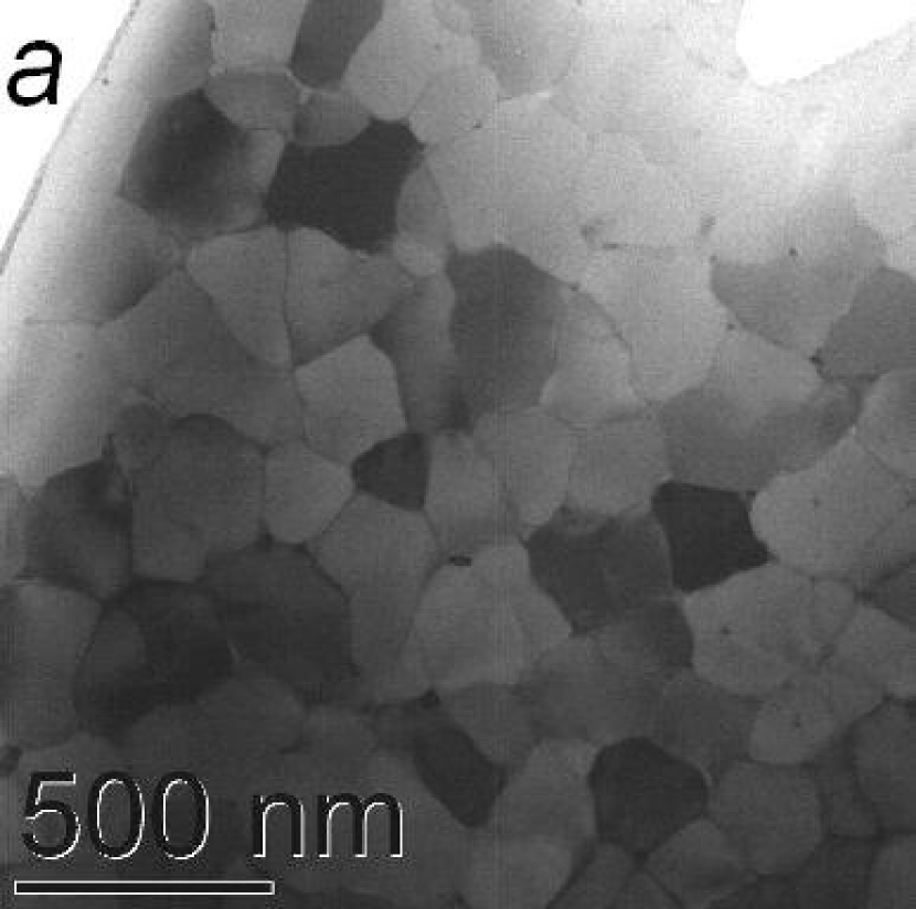
Both samples were meltspun with a wheel rotation speed of 1500 rpm. In sample A a small amount of foreign phase was detected. TEM investigations show that they form thin intergrain layers. Sample B was phase pure according to XRD (Fig. 1). TEM reveals only a tiny amount of foreign phases which are concentrated at the junctions of three grains, the boundaries between two grains being free of any intergrain phase. This is why we focussed our further investigations on sample B. Most importantly, the meltspun sample B has a much smaller grain size (about 200 nm) than the meltspun parent phase Ba8Ga16Ge30 (about 1000 nm), as shown by TEM images (Fig. 2) [14].
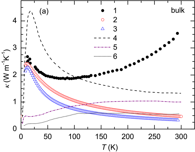
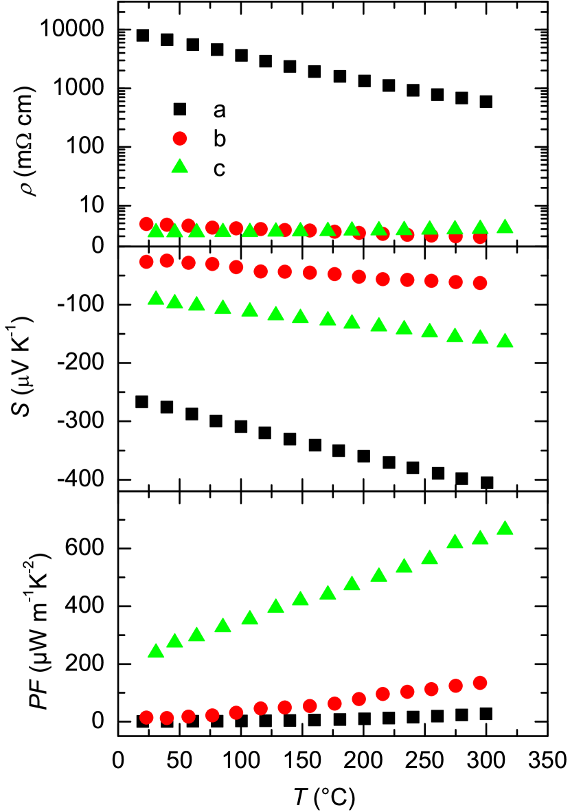
In the obtained 9-element clathrate, three “phonon engineering” approaches are believed to be combined: (i) the intrinsically low thermal conductivity of clathrates [23, 24], (ii) the alloying effect, and (iii) the grain size reduction. Unfortunately we could not yet perform reliable thermal conductivity measurements on the rather brittle meltspun 9-element clathrate flakes to evidence the effect of this triple-phonon engineering approach. Here we present only the thermal conductivity of the bulk nine-element clathrate phase prior to melt spinning. Thus only the alloying effect on the lattice thermal conductivity is demonstrated (Fig. 3, a). The lattice thermal conductivity obtained after substraction of the electronic contribution and a radiation term is extremely low. For comparison, the lattice thermal conductivities of Ba8Ga16Ge30, Sr8Ga16Ge30, and Eu8Ga16Ge30 adopted from [25] are shown. In Fig. 3, b the power factor of the bulk sample is presented in the temperature range 300 - 440 K. The room temperature of sample B amounts to about 0.07.
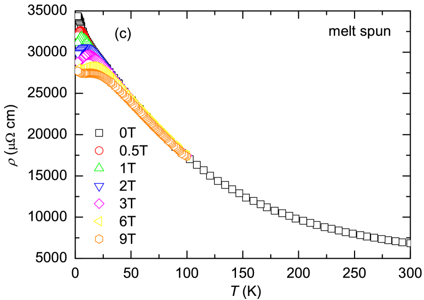
By contrast, we did succeed to measure the electrical resistivity of the meltspun 9-element clathrate sample B. It shows semiconducting behavior (Fig. 3, c). Below 30 K, decreases with increasing magnetic field, presumably due to a reduction of electron scattering from Eu2+ magnetic moments which order ferromagnetically at about 20 K, as evidenced by measurements of the magnetic susceptibility (not shown).

2.4 Electron microscopy investigation of meltspun clathrates
As described above, our efforts to reduce the grain size of clathrates by melt spinning were only moderately successful. To understand this unusual crystallization behavior of clathrates we performed a more detailed investigation. We studied the rapid crystallization of clathrates with the starting compositions Ba8Au5Si41 and Ba8Ni3.5Si42.5. The meltspun samples were brittle thin ribbons of the typical size of mm3 (flakes). The microstructure of the polished flake surfaces and of the flake cross-sections was investigated by SEM and TEM.
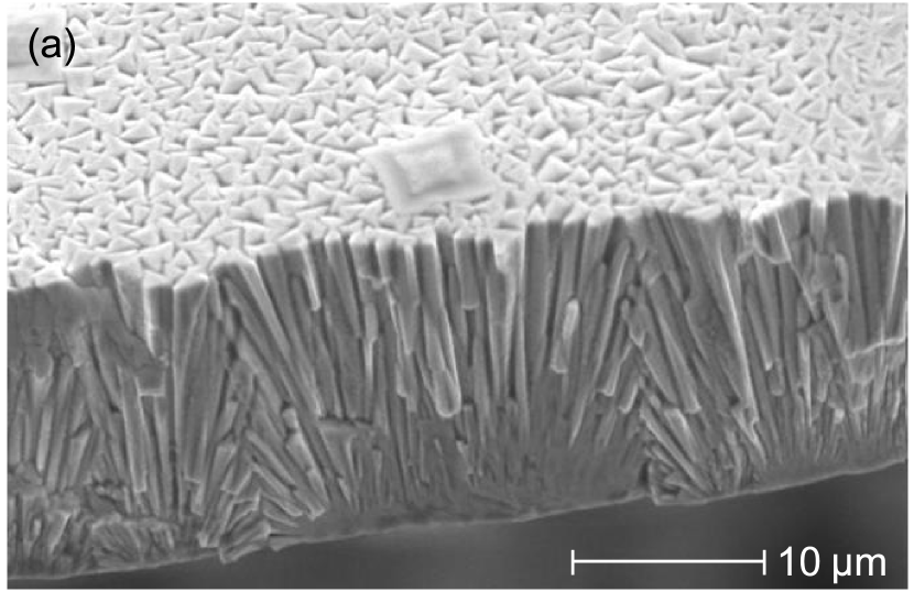
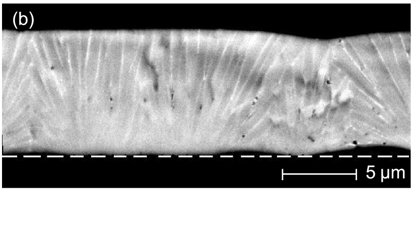
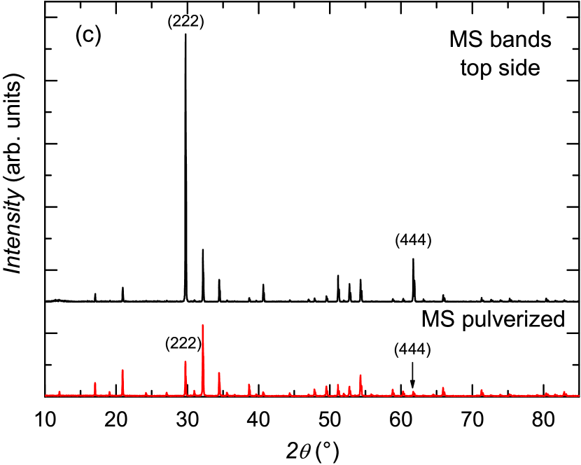

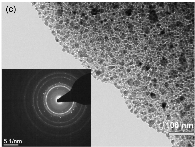
Inspecting flake cross-sections helps us to understand much of the time-resolved growth process. Both as-broken and polished surfaces reveal columnar crystallite growth (Fig. 4 a, b and 5 b). The preferential crystal growth direction is [111], as seen from the comparison of the XRD patterns of the intact as-spun and the pulverized flakes (Fig. 4 c). Despite the overall micro-sized grain picture of the meltspun samples, the very bottom (contact surface) part contains a thin diffuse-looking layer of material which is featureless in SEM. A high-resolution TEM investigation of this layer in meltspun Ba8Ni3.5Si42.5 supported its crystallinity and nanogranular structure with grain sizes of 10 - 40 nm (Fig. 5 c). These features of the microstructure shed light on one of the reasons for the coarse microstructure of the meltspun clathrate. Crystalline clathrates have an extremely low thermal conductivity. As soon as a thin layer near the cooling surface crystallizes it impedes further heat flow, and the effective cooling rate drops for the remaining layer of melt.
However, one more reason may underlie the formation of large grains [26]. In complex polar liquids such as water solutions of ionic compounds the formation of pentagonal dodecahedron clusters was revealed [27]. Despite the very different chemical nature of water solutions and “clathrate melts” their structural similarities are obvious – both water molecules and group-IV elements, which dominate the melt, have a strong tendency to form tetrahedrally bonded networks. This similarity is supported by the existence of solid water clathrates, e.g. the methane hydrate (CH4)8(H2O)46. In water solutions of ionic compounds such clusters are formed around the positive ion (“ionic clathrates”) [27]. The small cage of a type-I clathrate structure is a pentagonal dodecahedron too. Thus a fragment of the clathrate structure is already present intrinsically in the clathrate melt if we assume its similarity with water. This may be the reason why the clathrate phase is preselected in a rapid solidification process among all other competing phases with crystallographic types of local symmetry. Since the pentagonal dodecahedron which is responsible for this process is also present in clathrates of types I to III and IX [28] similar behavior is expected also for these clathrates. It is the early nucleation that possibly also leads to large grains: if the nucleation was strongly retarded to a lower temperature when the crystal growth was already suppressed due to a low diffusion rate, nanoscale grains would form [26].
2.5 Melt spinning of Ba8Cu5Si6Ge35-xSnx
Even though melt spinning does not readily produce nanostructured clathrates, it is advantageous to produce clathrate phases with broader composition ranges than what is possible by conventional synthesis techniques [8, 9]. The main motivation of this study was to increase the solubility limit of Sn in Ba8Cu5Si6Ge35-xSnx clathrates to improve their thermoelectric properties. We expected a partial Ge substitution by heavier Sn to lower the thermal conductivity, which was indeed realized. In addition, the change of the electronic structure shifted the maximum of to lower temperatures [29].
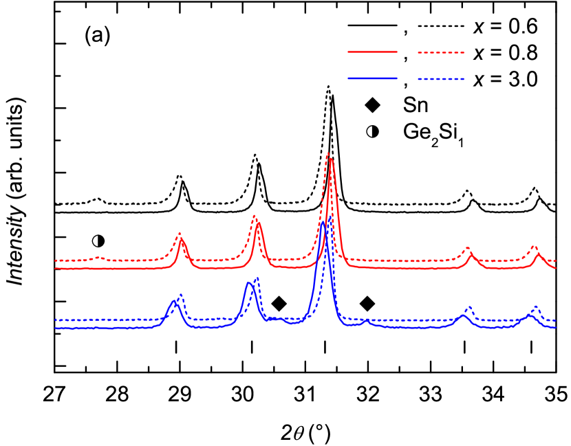
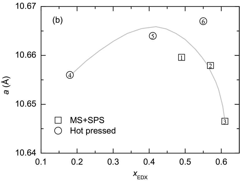
Polycrystalline samples with the nominal compositions Ba8Cu5Si6Ge35-xSnx (x = 0.6 3.0) were prepared using melt spinning and spark plasma sintering (SPS). According to XRD, all meltspun (MS) samples are type-I clathrate phases with a small amount of Sn as impurity phase (Fig. 6 a). During the SPS process a small amount of diamond phase Ge2Si forms while the Sn impurity phase disappears. The composition of the MS+SPS samples evaluated from EDX, their relative densities, and their lattice parameters are shown in Table 2. The maximum amount of Sn in the type-I clathrate phase is approximately 0.6 at./u.c. which, unfortunately, is only slightly larger than the value reported in Ref. [29] (see also Table 2). The Cu content decreases with increasing x. This, together with an appearance of vacancies, influences the electrical transport. All MS+SPS samples are well compacted, with relative densities between 93 % and 98 %. Figure 6 b shows that the substitution of Ge by larger Sn atoms increases the lattice parameter in the hotpressed samples with a low substitution level . However, in the MS+SPS samples with a higher substitution level, decreases with further increasing . We assume that the latter is due to the decrease of the (Cu+Ge)/(Si) ratio, as Cu and Ge are larger than Si.
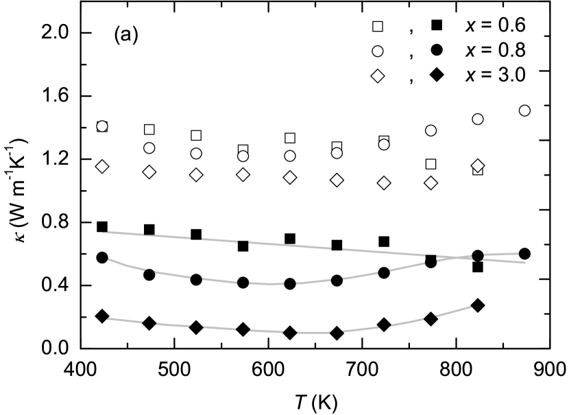
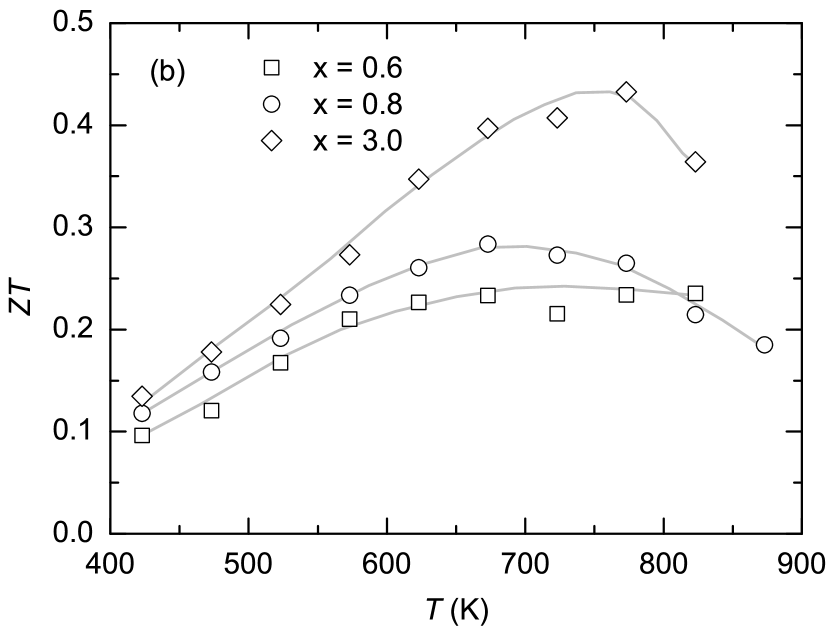
The temperature dependence of the thermal conductivities of all samples and their phonon contributions are shown in Fig. 7 a. decreases with increasing temperature up to about 650 K. Above this temperature a bipolar contribution is observed, as in the case of the hotpressed samples (Ref. [29]). The decrease of at low temperatures can be understood as the combined effect of Umklapp scattering of acoustic phonons () and alloy scattering (). The decrease of with higher is most probably due to the higher Sn concentration and a larger vacancy content. At 750 K, of the MS+SPS samples is only half of the value of the hotpressed samples [29]. The dimensionless figure of merit is 0.43 at 773 K for x = 3.0 (Fig. 7b).
| x | Code | Composition | a | (Cu+Ge)/(Si) | d |
|---|---|---|---|---|---|
| (nm) | () | ||||
| 0.6 | 1 | Ba8Cu5.23Si6.43Ge33.68Sn0.48 | |||
| 0.8 | 2 | Ba8Cu5.21Si6.79Ge33.34Sn0.57 | |||
| 3.0 | 3 | Ba8Cu5.06Si7.46Ge32.76Sn0.60 | |||
| 0.2 | 4 | Ba8Cu4.98Si5.88Ge34.76Sn0.18 | |||
| 0.4 | 5 | Ba8Cu4.92Si5.92Ge34.57Sn0.41 | |||
| 0.6 | 6 | Ba8Cu5.01Si5.93Ge34.28Sn0.55 |
2.6 Melt spinning of the skutteridite CoSb3
The unusual crystallization behavior of clathrates described in Sects. 2.2-2.4 poses the question whether it is unique for clathrates or typical also for other cage compounds with intrinsically low thermal conductivities. Which of the suggested mechanisms discussed in Sect. 2.4 – the suppression of the heat flow or the peculiarity of the crystal structure – is the dominant one? To answer this question we performed a similar investigation of melt spinning on the skutterudite CoSb3. We demonstrate that for CoSb3 melt spinning can be successfully used for nanostructuring.
We produced a series of meltspun and subsequently spark plasma sintered (SPS) CoSb3 samples, differing only by the cooling speed during the quenching procedure. Table 3 summarizes details for all samples studied here. The series consists of five different CoSb3 samples produced at various rotation speeds (600 - 3000 rpm) of the quenching copper wheel. After the melt spinning procedure all materials were compacted using SPS at a temperature of 550∘C and a pressure of 40 MPa for 5 minutes. The samples are named according to the rotation speed of the copper wheel during the melt spinning procedure (e.g., 600RPM).
| Code | Impurities | GS (XRD) | GS (TEM) | ||
|---|---|---|---|---|---|
| (rpm) | (Å) | (nm) | (nm) | () | |
| 600RPM | Sb | ||||
| 1200RPM | CoSb2 | ||||
| 1800RPM | CoSb2 | ||||
| 2400RPM | CoSb2 | ||||
| 3000RPM | CoSb2 |
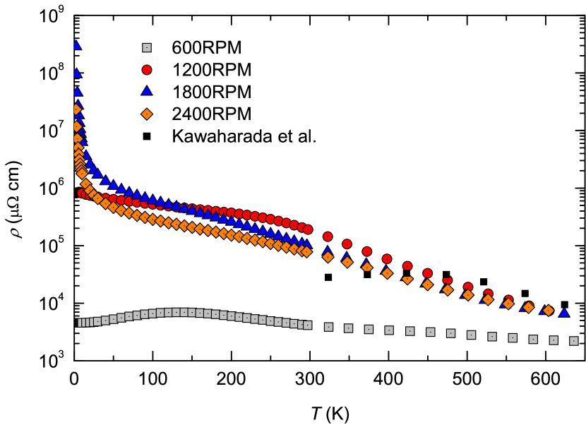
XRD on the meltspun CoSb3 samples resulted in a phase mixture with CoSb3 as the majority phase and Sb and CoSb2 impurity phases in all meltspun samples [18]. This is consistent with the fact that CoSb3 melts incongruently. In contrast to type-I clathrates, the crystallization rate of CoSb3 is too small for the kinetic suppression of foreign phases. In line with studies on meltspun filled skutterudites [10, 11, 12], the content of foreign phases is readily reduced by the heat treatment during the SPS procedure. A small amount of Sb in 600RPM and CoSb2 (see Tab. 1) was, however, detected by XRD investigations even in the sintered samples. Due to the relatively large amount of CoSb2 in the sample 3000RPM, this material is not considered in the discussion presented below.
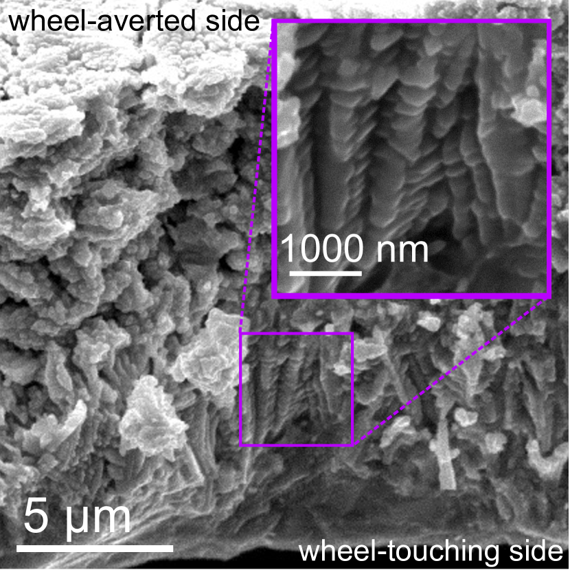
Figure 8 shows the broken cross-section of a meltspun CoSb3 flake of the batch 1200RPM. In contrast to type-I clathrates [30, 26], the meltspun CoSb3 samples consist of nearly spherical grains. This is the case even for the seemingly columnar areas on the wheel-touching side (Fig. 8 inset). In contrast to type-I clathrates, which show columnar grain growth, the rate of crystallization and the speed of grain growth is thus found to be moderate.
 \subfloat
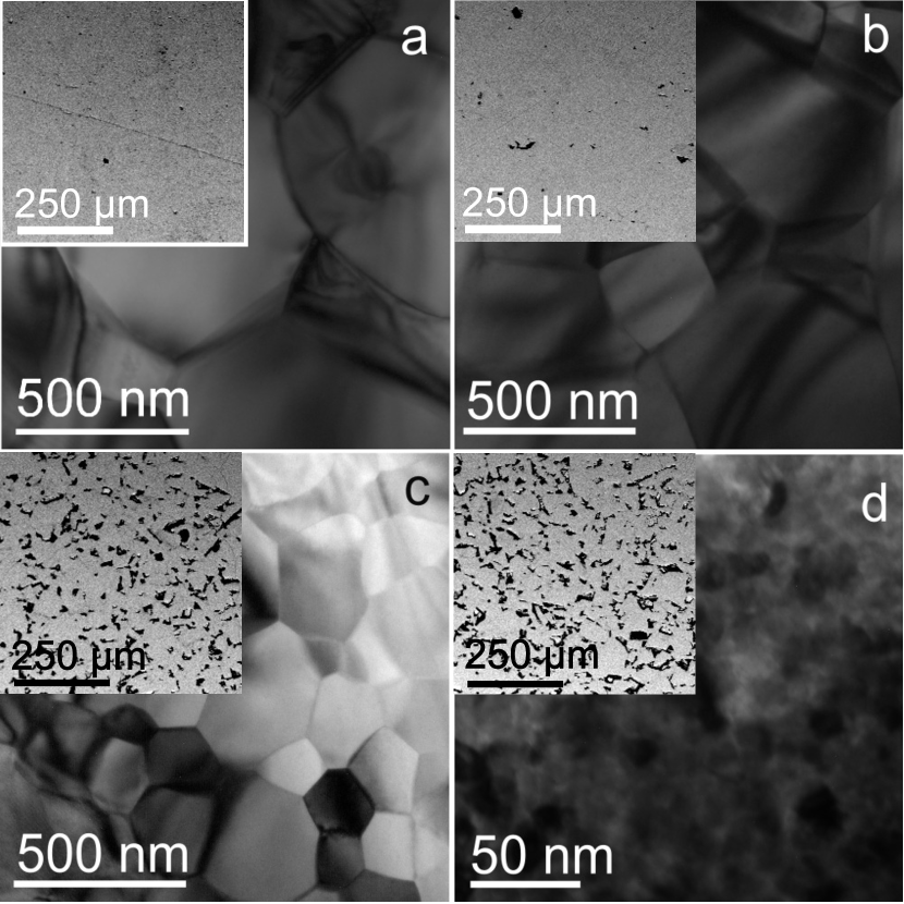
TEM investigations on the samples 600RPM, 1200RPM, 1800RPM, and 2400RPM after the SPS procedure clearly evidence that the grain size of the materials is dependent on the cooling rate during melt spinning. The grain size determined by TEM and, alternatively, by XRD is summarized in Tab. 3. The discrepancy observed for 2400RPM is most likely explained by the presence of regions with different grain sizes. The insets of Fig. 9 show SEM pictures of the materials 600RPM to 2400RPM. The incomplete compaction of 1800RPM and 2400RPM, indicated by the lower measured relative densities (Tab. 3), is also clearly observed in the corresponding SEM pictures.
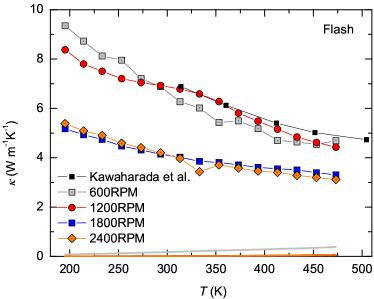
The thermal conductivity of the meltspun and SPS samples was studied by two different techniques. First, the thermal conductivity was determined from the measured room temperature density , the thermal diffusivity , and the specific heat (Ref. [18]) according to . The result is shown in Fig. 10 (left). Within the resolution of our Flash experiment, the phonon contribution of 600RPM and 1200RPM is similar. 1800RPM and 2400RPM show a significantly reduced thermal conductivity. Unfortunately these samples not only possess a smaller grain size compared to 600RPM and 1200RPM, but also an approximately 10 % lower relative density (Tab. 1). Thus, the mechanism of the reduction cannot be pinned down from these results.
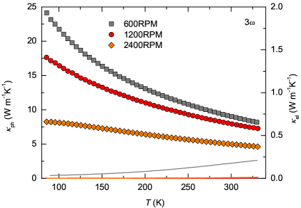
Therefore, we studied the thermal conductivity of the meltspun and SPS samples in more detail using additional 3 thermal conductivity measurements. As long as the sample surface is sufficiently flat, the heater geometry can be determined with high accuracy. For porous materials on the other hand, the length of the heater can considerably deviate from its nominal value. This introduces an error in the measured thermal conductivity, because the line power density is a multiplicative quantity for calculating the in-phase temperature oscillation. As observed for the sample 1800RPM, moreover the insulating layers between heaters and porous samples are likely to show pinholes. In such cases, accurate 3 measurements cannot be performed. The overall trend of our 3 phonon thermal conductivity data is similar to the Flash thermal conductivity results but the absolute values are systematically higher. Since the absolute values of the 3 measurements on the dense samples 600RPM and 1200RPM can be considered as accurate the Flash data appear to underestimate . In agreement with the decreasing grain size the 3 values are found to decrease with increasing rotation speed. Due to the incomplete compaction of 2400RPM, its low values can, however, not be fully attributed to scattering on additional grain boundaries. The difference in the values among all meltspun and SPS treated CoSb3 samples increases towards lower temperatures. This is in agreement with the increase of the phonon mean-free-path associated with the freezing of Umklapp processes upon cooling.
Figure 11 shows the electrical resistivity of all investigated CoSb3 samples as a function of temperature. 1200RPM, 1800RPM, and 2400RPM show semiconducting behavior in the entire temperature range. 600RPM, however, shows features of weak metallicity at low temperatures. By studying magnetoresistance and Hall effect data of the presented sample series in terms of a multiband model, we attributed the decrease of the electrical resistivity of 600RPM to additional charge carriers with high carrier mobility introduced by the Sb foreign phase [18]. A surprising result is that the poorly compacted materials 1800RPM and 2400RPM show similar resistivities as the well compacted sample 1200RPM. A reason for this behavior might be the SPS mechanism: the compaction is achieved by pressure and heat generated by an electrical current flowing through the material. Thus, even in samples with low densities there are continuous low-resistance current paths through the sample.
3 Ball milling and hot pressing
3.1 Nanostructuring by ball milling
Nanostructured bulk materials can also be obtained by ball milling. This top-down nanostructuring technique is generally considered as a simple, economic, and efficient method that has been used frequently in different intermetallic systems [32, 33]. The fundamental mechanism for powder refinement during this process is to use the kinetic energy of the mill system to fragmentate large particles to small ones [32]. The particle size in powders is determined by the milling energy, milling time, and other process parameters (e.g., the atmosphere and choice of additives) as well as the mechanic properties of the raw materials [32, 33, 34, 35, 36].
Studies of crystallite size vs milling time were carried out on clathrates in the Ba-Cu-Ge-Si system. Our previous investigation on Ba8Cu5SixGe35-x showed that the best thermoelectric performance was found in compounds with low [29]. Thus, we chose the composition Ba8Cu4.5Si6Ge35 for further investigations [37].
The ball milling was performed in a Fritsch planetary mill. Pre-synthesized and annealed (, 20 days) large samples (4 g each) were used for ball milling. The process parameters were as follows: speed of the main disk = 120 rpm, weight ratio of balls to powders = 82, planetary ratio = -2.5, ball diameter cm, material of containers and balls = WC. The milling time is denoted by .
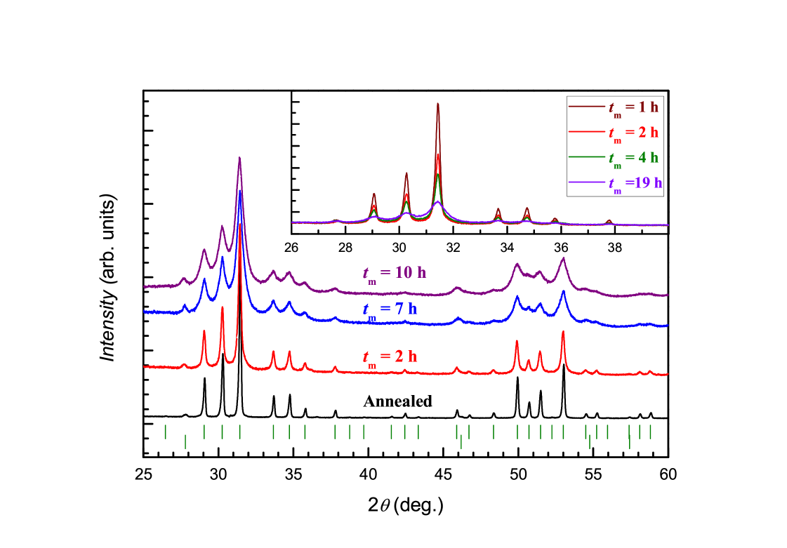
The phase analysis of the as-milled powders was performed using XRD. The XRD patterns of an annealed sample and several as-milled powders are shown in Fig. 12. The broadening of the peaks in the patterns of the as-milled samples arises from the reduced grain/crystallite size and increased residual strain after milling. No peak shift or new peaks appear in the patterns after milling, indicating that the phase composition is stable during the milling process.
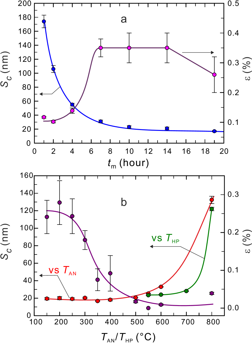
The crystallite size decreases rapidly in the first 4 h of the milling treatment, and approaches saturation slowly thereafter (Fig. 13 (a)). The minimum size after 19 h milling was nm. The residual strain , on the other hand, increases in the beginning, reaches a maximum of 0.35% after 7 h, and decreases slightly after 14 h. Our study indicates that a repeated powder separation from both the container and the balls is necessary during the ball milling process; without this separation the minimum crystallite size after 14 h reaches only 45(5) nm. The powders without and with powder separation are referred to as batch I and batch II in what follows.
To determine the best hot pressing temperature, a study of crystallite size growth/strain reduction was carried out by annealing the nanopowders in vacuum at different temperatures for 2 h. The crystallite size of powder from batch II remains essentially unchanged when the annealing temperature is below but the residual strain is released (Fig. 13 b). Above , the crystallite size increases rapidly. This suggests that the pressing temperature should not exceed to keep the grains small.
3.2 Consolidation by hot pressing
Powder consolidation is required to obtain bulk samples. Conventional pressureless sintering is often unable to provide dense materials with very fine grains [38]. Pressure-assisted sintering methods such as hot pressing, hot isostatic pressing, or spark plasma sintering have thus been at focus [33, 39]. The process parameters are pressure, pressing temperature, holding times, heating rate, and atmosphere for sintering. They determine the microstructure and the physical and mechanical properties of the sintered samples.
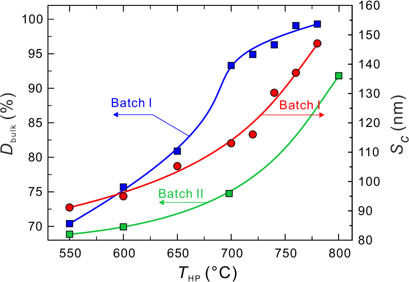
We focused on the effect of the hot pressing temperature on the microstructure and the thermoelectric properties of sintered samples [40]. We fixed the pressure MPa, holding time h, and heating rate /min during the hot pressing process. Since the properties of the hotpressed samples are also determined by the properties of the nanopowders for sintering, we studied the two above-discussed batches of nanopowders which have different crystallite size (45(5) nm for batch I, 18(1) nm for batch II). We chose pressing temperatures between 550 and (Fig. 13 b).
Figure 14 shows the crystallite size and relative bulk density of samples sintered from nanopowders of batch I vs the pressing temperature . Both and increase with . To obtain dense samples with small grain size, should be between and . The qualitative behaviour of batch II is similar (Figs. 13 b and 14).
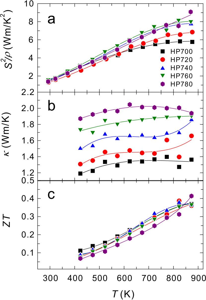
Below 850 K, the values of the samples sintered with are higher than for the sample sintered with . As all samples have similar power factor this is mainly attributed to the lower thermal conductivity caused by the smaller grain size (Fig. 15).
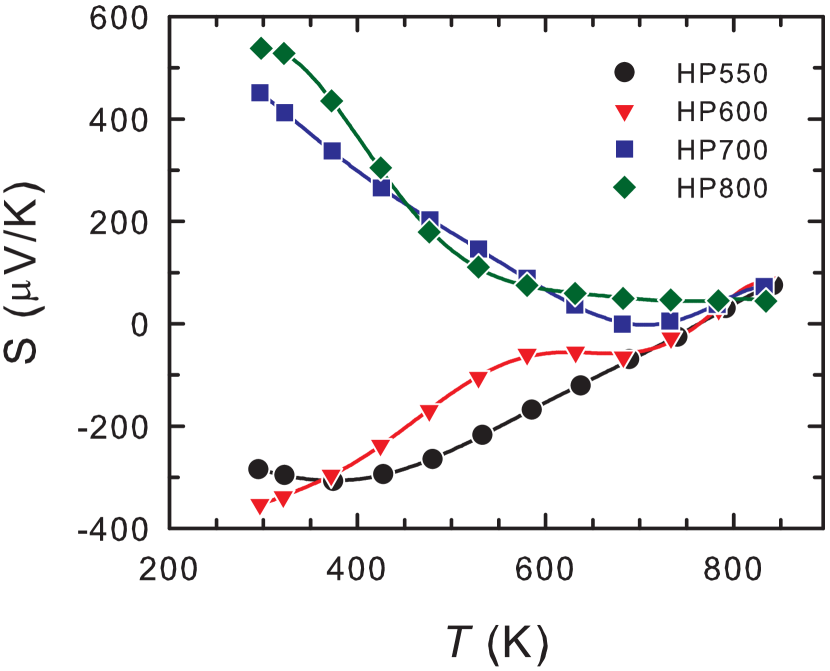
hotpressed samples using powder from batch II behave quite differently in terms of stability and thermoelectric properties [37]. Firstly, the phase composition is not stable during the hot pressing process, as evidenced by the change of the lattice parameter of the clathrate phase and the increase of the peak intensity of the diamond phase with (Fig. 16). Secondly, all samples show semiconducting behavior with high electrical resistivities between 0.5 and 4 cm at room temperature. The values are below 0.05 for all samples (not shown). Additionally, the samples with the lowest bulk densities are unstable during the transport measurements at high temperatures. All this may at least in part be attributed to the composition instability.
The change of composition during hot pressing most likely leads to an increase of the Cu content and a decrease of the charge carrier concentration, leading to the observed increased electrical resistivity and absolute Seebeck coefficient values [41]. Within a rigid-band picture, this would shift the Fermi level first downwards to the lower edge of the conduction band, and then further downwards across the band gap to the top of the valence band. Indeed the Seebeck coefficient changes from negative to positive with increasing (Fig. 17).
Interestingly, the samples sintered from the finer powders of batch II have much lower than those of batch I (Fig. 14). This seems counterintuitive since finer powders should be easier to sinter due to their higher surface energy and larger contact areas between particles [38, 33, 39]. We suggest that the formation of contaminations during ball milling and composition changes during hot pressing consume surface energy. On the other hand, composition gradients between the shell and the core of small particles and contaminations on the particle surfaces prevent particle growth [39] and bonding between particles. Together, this leads to smaller grain sizes but lower bulk densities of the samples hotpressed from the powder of batch II.
The crystallite size of the samples hotpressed from the powder of batch II remains very small even for up to (Fig. 13 b). During annealing, a clear increase of the grain size sets in already at about . This indicates that pressure indeed suppresses grain growth.
Based on the above results, we considered to use a process control agent during ball milling to inhibit powder agglomeration, to use different powder consolidation techniques, and to form nanocomposites for clathrates. Also we simplified the clathrate from the optimized quaternary system to the ternary system Ba-Cu-Si.
3.3 Influence of process control agent
Samples of the nominal composition Ba8Cu4.8Si41.2 used for this investigation were previously shown to have the largest Cu solid solubility (at ) [42] and the best thermoelectric performance [41] within the ternary Ba-Cu-Si system. We used stearic acid, CH3(CH2)16CO2H, as a process control agent (PCA). The aim is to study how the PCA influences the behavior of grain size reduction during ball milling and growth during hot pressing [43, 44]. The process parameters for ball milling and hot pressing were fixed according to Sects. 3.1 and 3.2.
The powder yield, which is the fraction of powder that can be collected after the ball milling process, increases from 46% without the PCA to 98% with 3 wt.% PCA, confirming that the PCA indeed reduces agglomeration effectively (Fig. 18 (a)). It also largely facilitates the removal of the powders from the containers.
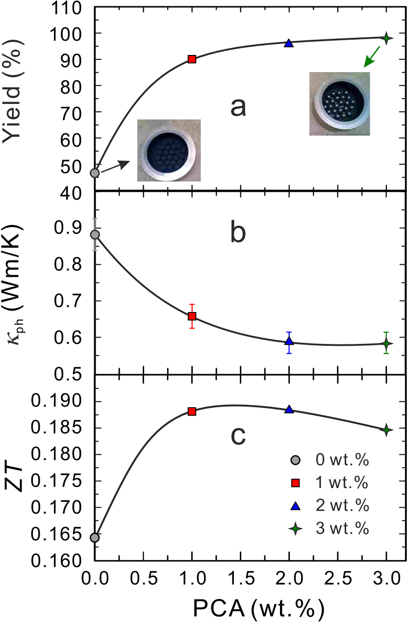
After 5 h milling treatment powders milled with the PCA have nm, which is lower than for powders milled without the PCA (70 nm) if the powders are not repeatedly manually separated from the balls and containers (batch I). However, it is larger than the reached in batch II (with manual powder separation). Thus the PCA is not as effective as mechanical separation. Longer milling times might be required.
We had expected the stearic acid to evaporate during powder sintering by hot pressing at because its boiling temperature is . However, TEM revealed very thin (5 nm) carbon layers around the grains. This suggests that the stearic acid has (partially) decomposed into carbon and gases to form these layers. They effectively prevent grain growth during hot pressing, leading to lower thermal conductivities (Fig. 18 b), but are also responsible for increased electrical resistivities. The values of the PCA-containing samples are overall higher than that of the PCA-free sample in the whole temperature range (by 15% higher at ). The sample with 2 wt.% PCA has the lowest lattice thermal conductivity (Fig. 18 b).
3.4 Powder consolidation by spark plasma sintering
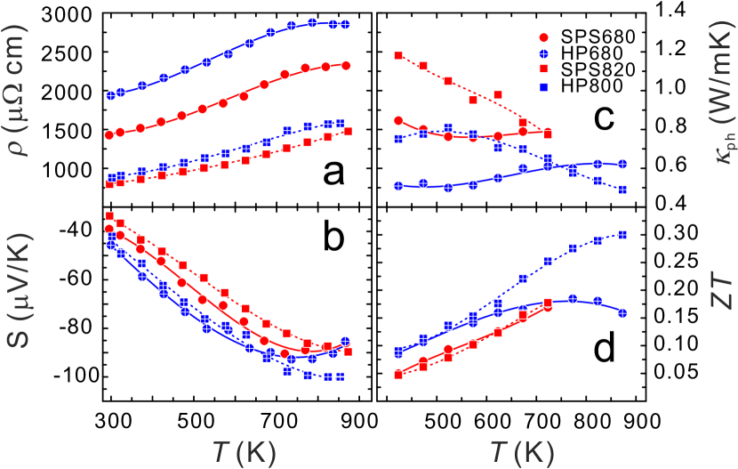
Spark plasma sintering (SPS) represents a promising powder consolidation technique for the rapid densification at relatively low temperatures. An electrical current is forced to flow through the sample during heating [38, 45]. The low temperatures and short holding times are ideal to limit grain growth. Compounds for this study [46] again have the nominal composition Ba8Cu4.8Si41.2. This study was performed at the laboratory for Solid State Chemistry and Catalysis at EMPA, where annealed samples were ballmilled and the as milled powders were sintered by SPS. In parallel, annealed samples from the same batch were also ballmilled at the Institute of Physical Chemistry at the University of Vienna and the as milled powders were sintered by hot pressing. Unfortunately, because of the different ball milling systems and different process parameters for milling, the nanopowders had different grain/crystallite sizes: nm for the powders for the SPS treatment and nm for the powders for hot pressing.
Presumably due to the smaller crystallite size of the nanopowders, the samples sintered by hot pressing have higher bulk densities and lower crystallite sizes than the samples sintered by SPS with the same sintering temperature. In addition, a white phase forms during the SPS process, which is rarely observed in hotpressed samples. This white phase has a high Cu content and thus the Cu content in the clathrate phase is reduced. The SPS treated samples have lower and than the hotpressed samples (Fig. 19). The hotpressed samples have higher than the SPS treated samples. Also the bulk density plays an important role. The highest of 0.3 at 870 K is reached in a sample with a very high bulk density of 99%.
4 Nanocomposites
A limitation of bulk nanostructured thermoelectric materials is their thermal instability with respect to coarsening. An approach to overcome this problem is to use bulk nanostructured composites in which one of the constituting phases serves as spacer between the nanograins of the active thermoelectric medium. To prevent coarsening the spacer and active material should be of different chemical nature. Here we studied two different spacer materials, thermoelectric oxides and SiC.
4.1 Clathrate-oxide nanocomposites
Ideally, the spacer material is itself a thermoelectric material. Therefore, in a first step, we chose thermoelectric oxides. The first task was to find a pair of mutually chemically inert materials. Among a series of thermoelectric oxides the system EuTiO3-δ was selected because it shows no traces of chemical reaction with the clathrate phases Ba8Pd4Ge40 and Ba8Ga16Ge30 selected for this study up to 800∘C.
For the investigation of the coarsening two series of samples were prepared: a pure Ba8Ga16Ge30 nanostructured clathrate and the nanocomposite Ba8Ga16Ge30 + EuTiO3-δ (13%), both ballmilled and SPS compacted at Empa. The samples were thermally treated stepwise at 500 and 650∘C (20 hours), and the grain size was evaluated by XRD after each step (Fig. 20). At 500∘C the crystallite size of the pure clathrate material and the clathrate phase in the composite were nearly equal whereas after the treatment at 650∘C the clathrate phase in the composite sample showed about twice smaller crystallite size.
In Fig. 21 we compare the thermoelectric properties of the composite to those of the two constituents. The powerfactor of the composite is larger than that of the oxide, but smaller than that of the clathrate. This disappointing result is mostly due to the unexpectedly low thermopower of the composite. It is lower than that of both constituents, which suggests that at least one of the two phases was degraded by the mixing process. As XRD rules out the formation of sizable amounts of foreign phases a change in composition within the oxide or clathrate phase should be evoked. Indeed, above 200∘C, the electrical resistivity of the composite is lower that that of both constituents, suggesting that the clathrate and/or the oxide are sizably doped in the composite. The strong effect 13 % oxide phase have on the composites properties is encouraging because it indicates that the oxide is very well distributed between clathrate grains. If the undesired doping effect can be suppresses, this route could thus prove useful.
4.2 Clathrate-SiC nanocomposites
Due to the above described undesired doping effect in the clathrate-oxide composites, the use of a passive spacer material was explored as an alternative route. For this purpose, we mixed ballmilled Ba8Cu4.8Si41.2 nanopowders with thermally and chemically stable SiC nanoparticles with a grain size of 40-50 nm. Different amounts of SiC (0, 1, and 3 wt.%) were first mixed with hand-ground clathrate powders and then ballmilled for 8 h. 2 wt.% of stearic acid was used as a process control agent (PCA) in all samples to prevent powder agglomeration.
| Code | HP.SiC0 | HP.SiC1 | HP.SiC3 |
|---|---|---|---|
| AM: (nm) | 36.2(5) | 40.6(4) | 35.7(6) |
| (%) | 0.18(1) | 0.13(1) | 0.18(1) |
| AS: (nm) | 69.0(5) | 75.5(6) | 70.9(6) |
| (%) | 0.006(1) | 0.005(1) | 0.015(1) |
| (%) | 96 | 90 | 92 |
| MHT: (nm) | 88.2(8) | 87(1) | 78(1) |
| (%) | 0.035(1) | 0.030(1) | 0.032(1) |
Table 4 gives the crystallite size , residual stress , and relative bulk density of samples in different states. of the as milled nanopowders is essentially independent of the amount of SiC. Thus the presence of SiC does not seem to influence the crystallite size. After sintering, is almost doubled but again independent of SiC. However, after high-temperature transport measurements, the sample with 3 wt.% SiC has a lower than the other two samples, indicating that the SiC particles reduced the grain growth of the host clathrate.
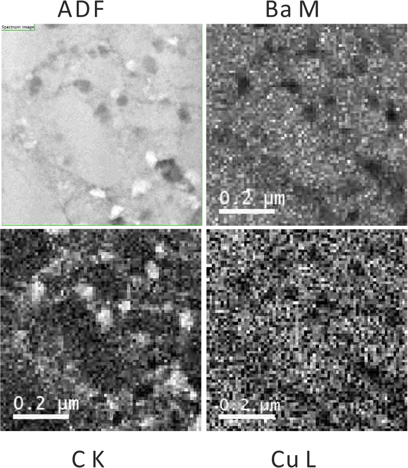
The grain growth behavior during powder sintering and thermoelectric property measurements at high temperatures might also depend on the amount and distribution of secondary phases in the host material. This effect was investigated by transmission electron microscopy (TEM). Figure 22 shows an annular dark field (ADF) image of the sample HP.SiC3 and element maps for the green square area measured by electron energy loss spectroscopy (EELS). As can be seen, Ba and Cu are uniformly distributed, evidenced by the quite uniform color in the maps, except for some black spots/bands. These correspond to white color in C (carbon) maps, indicating high C contents in these areas. The spots/bands correspondingly have black color in the ADF image. In this way we can identify the distributions of the C-rich phase(s) from ADF images.
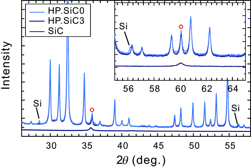
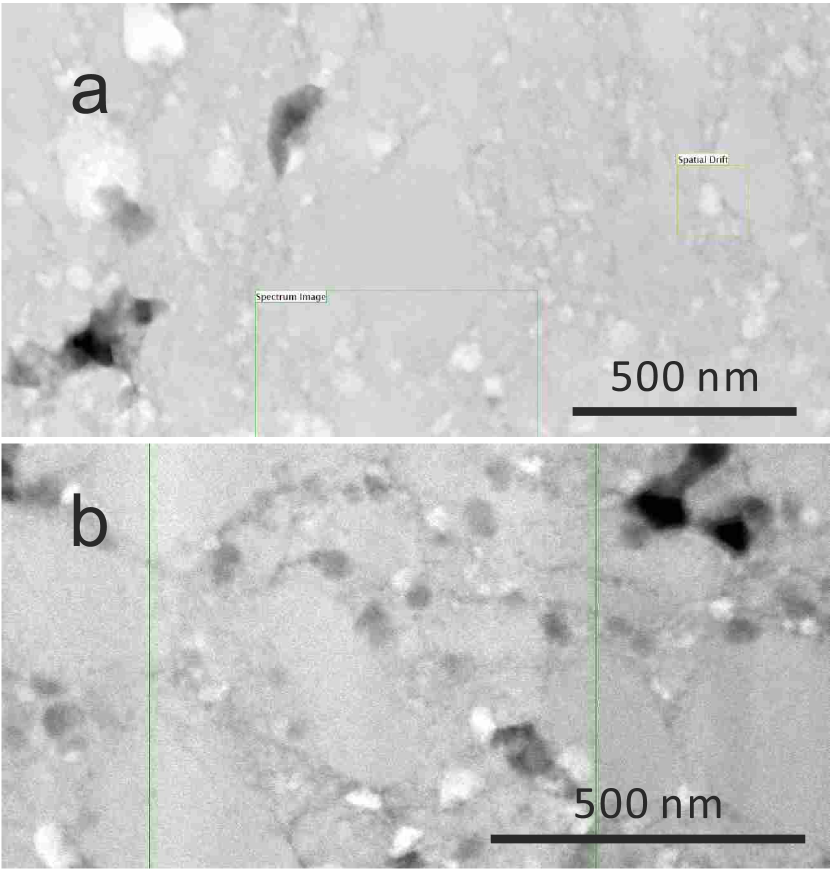
To measure the composition of the black phase by EDX is more difficult, especially with the attempt to confirm if the black phase is SiC, since Si also exists in the clathrate phase. By XRD, only from a very careful comparison of the patterns for HP.SiC0, HP.SiC3, and SiC, one can see tiny differences in shape and in intensity in the overlapped peaks of the clathrate phase and the SiC phase between HP.SiC0 and HP.SiC3 (Fig. 23). This indicates that SiC does not react with the clathrate phase and instead exists in the HP.SiC3 sample. Comparing the ADF images of HP.SiC0 and HP.SiC3 (Fig. 24) we conclude that the black phase of line/band-like shape, which can be also observed in the former sample, is the stearic acid (SA) and/or a phase decomposed from SA at high temperatures during hot pressing. The black phase in ball shape, which is only observed for the sample HP.SiC3, is SiC. From their different phase distributions – the SA phase surrounds the clathrate phase while SiC are distributed as separate grains – one can explain why the crystallite size is essentially independent of the SiC content. It is mostly the SA phase which determines the behavior of grain reduction and growth.
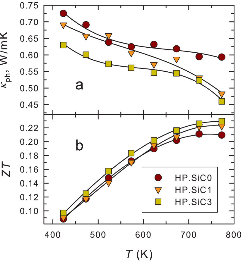
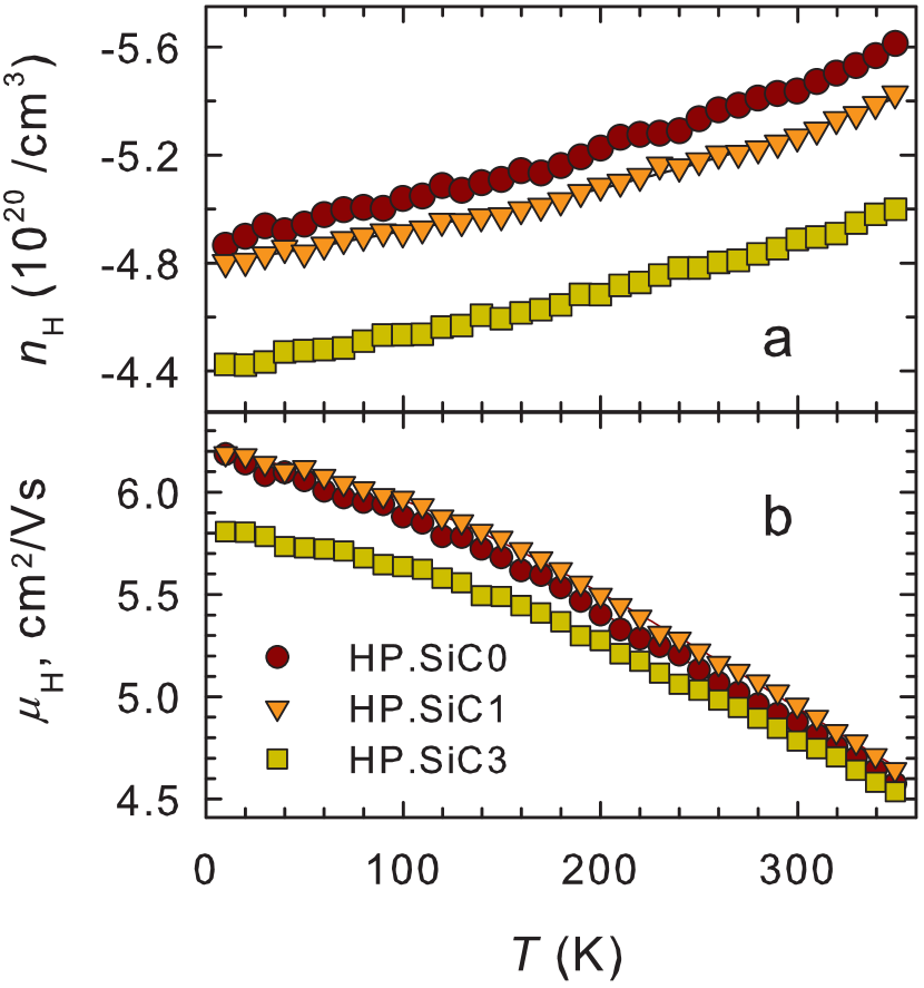
As a consequence of the SA phase around the nanoparticles, these samples have high electrical resistivity and low thermal conductivity compared with the samples prepared without SA during ball milling (see e.g., Fig. 25 and Fig. 19, HP800). The SiC nanoparticles add additional scattering centers and further reduce the lattice thermal conductivity (Fig. 25 a). These nanoparticles also scatter charge carriers, leading to a reduced charge mobility (Fig. 26 b), which plays a dominant role on the increased electrical resistivity. The Hall effect measurements revealed that the unexpectedly reduced charge carrier concentration in the HP.SiC3 sample is also held responsible for the high electrical resistivity. Correspondingly, the of this sample is higher than that of the other samples because of the lower charge carrier concentration (Fig. 26 a). The SiC-containing samples have slightly higher values due to the lower and higher (not shown).
5 Nanowires
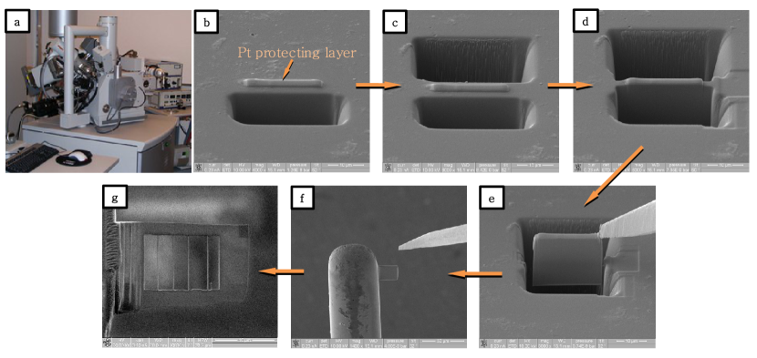
Understanding the effects of nanostructuring by investigations on bulk nanostructured materials is challenging because usually more than one parameter (e.g., grain size, material’s composition, doping level, amount of foreign phases) is changed at once. Thus it is advisable to study also simpler model systems. Here we report on our efforts to produce devices with clathrate nanowires of well-defined geometrical dimensions. Since there is no known route for the bottom-up fabrication of clathrate nanowires, we fabricate them with a top-down approach. In short, a focused ion beam (FIB) is used to sculpture nanowires out of a bulk starting material, which can be a single- or poly-crystalline sample with large enough grain size. This process is performed with the FEI Quanta 200 3D Dual Beam-FIB shown in Fig. 27a and proceeds as follows. The first step is to cut out a lamella such as is typically performed for transmission electron microscopy (TEM) sample preparation. To protect the sample surface, a platinum metal layer is deposited over the area of interest (Fig. 27b). Two trenches, one on each side of the metal line, are then carved out so as to define a lamella, which is then taken out using a lift-out technique by means of ’soldering’ the lamella to a micromanipulator needle with electron-beam induced deposition (EBID) of tungston, by tilting, and by further cutting the lamella free (Fig. 27c-e). Finally the lamella is transferred to a TEM grid (Fig. 27f). While this is, in essence, a standard technique, our process is taken one step further, and from the lamella nanowires are formed as evinced in Fig. 27g.
Inevitably, an amorphous surface layer is produced during FIB-cutting by the impinging Ga+ ions that have a typical energy of 30 keV and penetrate the top of the sample surface. This layer can however be thinned down by low-energy ( 1 keV argon (Ar+) milling. The whole process has been perfected such that we can produce micro- and nanowires with lengths of m and diameters of .
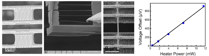
Figure 28, left, shows a microfabricated measurement platform similar to other published works [47, 48]. It consists of two separate silicon nitride membrane islands, across which the nanowire can be positioned. The islands are suspended by four beams that carry the input leads for the heaters, for the temperature sensors that are directly attached to the nanowire, and for the four-probe electrical measurements of the nanowire. The innermost electrodes serve both as voltage probes in the four-point measurements of the nanowire and as thermometer. The fabrication process involves dry etching and anisotropic KOH wet etching on the back side of the substrate. Contact pads are defined by photolithography, and leads, heaters, and electrodes are defined by electron beam lithography (EBL), as is the final etch mask that defines the islands and their supporting beams.
While we have not yet performed measurements on such a device, we managed to transfer a nanowire onto a thermoelectric nanowire characterization platform (TNCP) chip [49] as shown in Fig. 28, middle, again by means of EBID and FIB-cutting. Preliminary raw data for a room temperature Seebeck coefficient measurement on a Ba8Ga16Ge30 microwire are shown in Fig. 28, right. We also have built up a 3-setup for nanowires on which we plan to measure thermal conductivity in the near future.
6 Summary and conclusions
We have investigated the effect of nanostructuring on thermoelectric clathrates by different techniques: melt spinning, ball milling, composite formation, and the fabrication of single nanowires.
Our investigation of meltspun clathrates revealed that, at least with our current setup, clathrate flakes with grain sizes below 1 m do not form readily. They can, however, be enforced by additional actions such as severe alloying. This is in strong contrast to our findings for the skutterudite CoSb3, where a systematic dependence of the grain size and the lattice thermal conductivity on the cooling rate during the melt spinning process could be demonstrated. We attribute this difference to the extremely high formation rate of clathrates. This is also consistent with the fact that meltspun clathrates are essentially phase pure, whereas meltspun CoSb3 contains a sizable amount of foreign phases.
Ball milling, by contrast, is a very effective means to produce nanogranular clathrates with decreased lattice thermal conductivities. Here, the main challenge is to prevent grain growth during the compaction process. We studied in detail the influence of hot pressing parameters on the properties of the compacted bulk samples. The bulk density of the samples increases with increasing hot pressing temperature but at the same time the grains grow. Thus, the best hot pressing temperature can only be a compromise. We also studied the effect of a process control agent. It strongly enhances the powder yield during ball milling and reduces grain growth during hot pressing. Overall, an enhancement of the figure of merit by 15 % could be achieved with only 1 wt.% of stearic acid. Further improvements are expected if an agent can be found that leaves less traces after compaction.
To prevent grain growth during compaction and improve the long-term stability of nanostructured clathrates, we studied two different nanocomposites: a clathrate-oxide composite and a clathrate-SiC composite. Even though the constituent clathrate and oxide were selected because of their mutual phase stability, the composite showed much poorer thermoelectric performance than the clathrate alone. We speculate that this is due to a mutual doping effect at the clathrate-oxide interfaces. SiC by contrast is entirely inert and lead to a 10 % improvement of the figure of merit. The long term stability remains to be tested.
Finally, we set up a procedure to measure the thermoelectric properties of single clathrate nanowires. A clathrate nanowire is cut out of a macroscopic clathrate single crystal by the focused ion beam and argon milling technique, and placed on a suspended platform with integrated heaters and thermometers. The setup is now ready for measurements. In particular, clathrates with different nanowire diameter shall be studied. We expect the comparison of the size effect with theoretical calculations [50] to shed further light on the intrinsic thermal transport mechanisms, which will ultimately help to further optimize bulk nanostructured clathrates.
We thank A. Grytsiv for hot pressing and M. Waas for SEM/EDX investigations. The work was supported by the German Research Foundation (DFG project SPP 1386 nanOcla), the Austrian Science Fund (FWF project TRP 176 N22), the Christian Doppler Forschungsgesellschaft (CD-Labor für Thermoelektrizität), and the European Integrated Center for the Development of New Metallic Alloys and Compounds (C-MAC).
References
- [1] A. I. Boukai, Y. Bunimovich, J. Tahir-Kheli, J. K. Yu, W. A. Goddard Iii, and J. R. Heath, Nature 451, 168 (2008).
- [2] A. I. Hochbaum, R. Chen, R. D. Delgado, W. Liang, E. C. Garnett, M. Najarian, A. Majumdar, and P. Yang, Nature 451, 163 (2008).
- [3] G. Joshi, H. Lee, Y. Lan, X. Wang, G. Zhu, D. Wang, R. W. Gould, D. C. Cuff, M. Y. Tang, M. S. Dresselhaus, G. Chen, and Z. Ren, Nano Lett. 8, 4670 (2008).
- [4] Y. Ma, Q. Hao, B. Poudel, Y. Lan, B. Yu, D. Wang, G. Chen, and Z. Ren, Nano Letters 8(8), 2580–2584 (2008), PMID: 18624384.
- [5] B. Poudel, Q. Hao, Y. Ma, Y. Lan, A. Minnich, B. Yu, X. Yan, D. Wang, A. Muto, D. Vashaee, X. Chen, J. Liu, M. S. Dresselhaus, G. Chen, and Z. Ren, Science 320, 634 (2008).
- [6] X. W. Wang, H. Lee, Y. C. Lan, G. H. Zhu, G. Joshi, D. Z. Wang, J. Yang, A. J. Muto, M. Y. Tang, J. Klatsky, S. Song, M. S. Dresselhaus, G. Chen, and Z. F. Ren, Appl. Phys. Lett. 93, 193121 (2008).
- [7] A. J. Minnich, M. S. Dresselhaus, Z. F. Ren, and G. Chen, Energy Environ. Sci. 2, 466 (2009).
- [8] S. Laumann, M. Ikeda, H. Sassik, A. Prokofiev, and S. Paschen, J. Mater. Res. 26, 1861 (2011).
- [9] S. Laumann, M. Ikeda, H. Sassik, A. Prokofiev, and S. Paschen, Z. Anorg. Allg. Chem. 638, 294 (2012).
- [10] H. Li, X. Tang, X. Su, and Q. Zhang, Appl. Phys. Lett. 92, 202114 (2008).
- [11] H. Li, X. Tang, X. Su, Q. Zhang, and C. Uher, J. Phys. D: Appl. Phys. 42, 145409 (2009).
- [12] X. Su, H. Li, Y. Yan, G. Wang, H. Chi, X. Zhou, X. Tang, Q. Zhang, and C. Uher, Acta Mater. 60, 3536 (2012).
- [13] X. Tang, W. Xie, H. Li, W. Zhao, Q. Zhang, and M. Niino, Appl. Phys. Lett. 90, 012102 (2007).
- [14] A. Prokofiev, M. Ikeda, E. Makalkina, R. Svagera, M. Waas, and S. Paschen, J. Electr. Mater. 42, 1628–1633 (2013).
- [15] A. Prokofiev, S. Paschen, H. Sassik, S. Laumann, and P. Pongratz, utility patent AT: 10749 U1 2009-09-05, DE: 20 2008 006 946.7, patent applications US: 12/231,183, JP: 135994/2008 (2008).
- [16] D. G. Cahill, Rev. Sci. Instum. 61, 802 (1990).
- [17] D. G. Cahill and R. O. Pohl, Phys. Rev. B 35, 4067 (1987).
- [18] M. Ikeda, P. Tomeš, L. Prochaska, J. Eilertsen, S. Populoh, S. Löffler, R. Svagera, M. Waas, H. Sassik, A. Weidenkaff, and S. Paschen, Z. Anorg. Allg. Chem., in press (2015).
- [19] U. Aydemir, C. Candolfi, A. Ormeci, Y. Oztan, M. Baitinger, N. Oeschler, F. Steglich, and Y. Grin, Phys. Rev. B 84, 195137 (2011).
- [20] I. Zeiringer, M. Chen, A. Grytsiv, E. Bauer, R. Podloucky, H. Effenberger, and P. Rogl, Acta Mater. 60, 2324 (2012).
- [21] K. Klement, R. H. Willens, and P. Duwez, Nature 187, 869 (1960).
- [22] A. L. Greer, Science 267, 1947 (1995).
- [23] G. S. Nolas, J. L. Cohn, G. A. Slack, and S. B. Schujman, Appl. Phys. Lett. 73, 178 (1998).
- [24] J. L. Cohn, G. S. Nolas, V. Fessatidis, T. H. Metcalf, and G. A. Slack, Phys. Rev. Lett. 82, 779 (1999).
- [25] B. C. Sales, B. C. Chakoumakos, R. Jin, J. R. Thompson, and D. Mandrus, Phys. Rev. B 63, 245113 (2001).
- [26] A. Prokofiev, X. Yan, M. Ikeda, S. Löffler, and S. Paschen, J. Cryst. Growth 401, 627 (2014).
- [27] F. Sobott, A. Wattenberg, H. D. Barth, and B. Brutschy, Int. J. Mass Spectr. 185-187, 271–279 (1999).
- [28] P. Rogl, Thermoelectrics Handbook, (ed. D. M. Rowe, CRC Press, Boca Raton, 2006), chap. 32 (Formation and crystal chemistry of clathrates).
- [29] X. Yan, E. Bauer, P. Rogl, and S. Paschen, Phys. Rev. B 87, 115206 (2013).
- [30] A. Prokofiev, M. Ikeda, E. Makalkina, R. Svagera, M. Waas, and S. Paschen, J. Electron. Mater. 42, 1628 (2013).
- [31] Y. Kawaharada, K. Kurosaki, M. Uno, and S. Yamanaka, J. Alloys Compd. 315, 193 (2001).
- [32] C. C. Koch, Rev. Adv. Mater. Sci. 5, 91 (2003).
- [33] H. J. Fecht and Y. Ivanisenko, in Nanostructured Materials: Processing, Properties, and Applications (ed. C. C. Koch, William Andrew Publishing: 13 Eaton Avenue Norwich, NY 13815, 2006).
- [34] J. Eckert, J. C. Holzer, C. E. Krill, and W. L. Johnson, J. Mater. Res. 7, 1752 (1992).
- [35] C. C. Koch, Nano. Mater. 2(2), 109 (1993), cited By (since 1996) 408.
- [36] C.C.Koch, Nanostruct. Mater. 9(1-8), 13 (1997).
- [37] X. Yan, E. Bauer, P. Rogl, J. Bernardi, and S. Paschen, unpublished (2015).
- [38] T. Hungria, J. Galy, and A. Castro, Adv. Eng. Mater. 11(8), 615 (2009).
- [39] J. R. Groza, in Nanostructured Materials: Processing, Properties, and Applications (ed. C. C. Koch, William Andrew Publishing: 13 Eaton Avenue Norwich, NY 13815, 2006).
- [40] X. Yan, E. Bauer, P. Rogl, and S. Paschen, Phys. Stat. Solidi A 211, 1282–1287 (2014).
- [41] X. Yan, M. X. Chen, S. Laumann, E. Bauer, P. Rogl, R. Podloucky, and S. Paschen, Phys. Rev. B 85, 165127 (2012).
- [42] X. Yan, G. Giester, E. Bauer, P. Rogl, and S. Paschen, J. Electron. Mater. 39, 1634 (2010).
- [43] A. Zolriasatein, X. Yan, P. Rogl, A. Shokuhfar, and S. Paschen, J. Nano Res. 29, 121 (2014).
- [44] A. Zolriasatein, X. Yan, E. Bauer, P. Rogl, A. Shokuhfar, and S. Paschen, to appear in Mater. Design (2014).
- [45] Z. A. Munir, U. Anselmi-Tamburini, and M. Ohyanagi, J. Mater. Sci. 41(3), 763 (2006).
- [46] X. Yan, S. Populoh, E. Bauer, P. Rogl, and S. Paschen, to appear in J. Electron. Mater. (2015).
- [47] L. Shi, D. Y. Li, C. H. Yu, W. Y. Jang, D. Y. Kim, Z. Yao, P. Kim, and A. Majumdar, J. Heat Transfer 125, 881 (2003).
- [48] S. F. Karg, V. Troncale, U. Drechsler, P. Mensch, P. D. Kanungo, H. Schmid, V. Schmidt, L. Gignac, H. Riel, and B. Gotsmann, Nanotechnology 25, 305702 (2014).
- [49] Z. Wang, M. Kroener, and P. Woias, Sensors and Actuators A 188, 417 (2012).
- [50] G. K. H. Madsen, A. Katre, C. Bera, and A. Togo, Phys. Status Solidi A, this issue.