2Kavli Institute for Cosmological Physics, University of Chicago, 5640 South Ellis Avenue, Chicago, IL, 60637, USA
3School of Physics and Astronomy, Cardiff University, Cardiff CF24 3YB, United Kingdom
4Kavli Institute for Particle Astrophysics and Cosmology, Stanford University, 452 Lomita Mall, Stanford, CA, 94305, USA
5SLAC National Accelerator Laboratory, 2575 Sand Hill Road, Menlo Park, CA, 94025, USA
6Department of Physics, University of California, Berkeley, CA, 94720, USA
7High-Energy Physics Division, Argonne National Laboratory, 9700 South Cass Avenue., Argonne, IL, 60439, USA
8Department of Astronomy and Astrophysics, University of Chicago, 5640 South Ellis Avenue, Chicago, IL, 60637, USA
9Enrico Fermi Institute, University of Chicago, 5640 South Ellis Avenue, Chicago, IL, 60637, USA
10Department of Physics, University of Chicago, 5640 South Ellis Avenue, Chicago, IL, 60637, USA
11Department of Physics and McGill Space Institute, McGill University, 3600 Rue University, Montreal, Quebec H3A 2T8, Canada
12NIST Quantum Devices Group, 325 Broadway Mailcode 817.03, Boulder, CO, 80305, USA
13Materials Sciences Division, Argonne National Laboratory, 9700 South Cass Avenue, Argonne, IL, 60439, USA
14Canadian Institute for Advanced Research, CIFAR Program in Gravity and the Extreme Universe, Toronto, ON, M5G 1Z8, Canada
15CASA, Department of Astrophysical and Planetary Sciences, University of Colorado, Boulder, CO, 80309, USA
16Department of Physics and Astronomy, University of California, Los Angeles, CA, 90095, USA
17Department of Physics, Center for Education and Research in Cosmology and Astrophysics, Case Western Reserve University, Cleveland, OH, 44106, USA
18Department of Astronomy, University of Illinois at Urbana-Champaign, 1002 West Green Street, Urbana, IL, 61801, USA
19Harvey Mudd College, 301 Platt Boulevard., Claremont, CA, 91711, USA
20Department of Physics, University of Colorado, Boulder, CO, 80309, USA
21University of Chicago, 5640 South Ellis Avenue, Chicago, IL, 60637, USA
22Deptartment of Physics, Stanford University, 382 Via Pueblo Mall, Stanford, CA, 94305, USA
23Physics Division, Lawrence Berkeley National Laboratory, Berkeley, CA, 94720, USA
24Dunlap Institute for Astronomy & Astrophysics, University of Toronto, 50 St. George Street, Toronto, ON, M5S 3H4, Canada
25Three-Speed Logic, Inc., Vancouver, B.C., V6A 2J8, Canada
26Harvard-Smithsonian Center for Astrophysics, 60 Garden Street, Cambridge, MA, 02138, USA
27Department of Astronomy & Astrophysics, University of Toronto, 50 St. George Street, Toronto, ON, M5S 3H4, Canada
28Department of Physics, University of Illinois Urbana-Champaign, 1110 West Green Street, Urbana, IL, 61801, USA
Performance of Al-Mn Transition-Edge Sensor Bolometers in SPT-3G
Abstract
SPT-3G is a polarization-sensitive receiver, installed on the South Pole Telescope, that measures the anisotropy of the cosmic microwave background (CMB) from degree to arcminute scales. The receiver consists of ten 150 mm-diameter detector wafers, containing a total of transition-edge sensor (TES) bolometers observing at 95, 150, and 220 . During the 2018-2019 austral summer, one of these detector wafers was replaced by a new wafer fabricated with Al-Mn TESs instead of the Ti/Au design originally deployed for SPT-3G. We present the results of in-lab characterization and on-sky performance of this Al-Mn wafer, including electrical and thermal properties, optical efficiency measurements, and noise-equivalent temperature. In addition, we discuss and account for several calibration-related systematic errors that affect measurements made using frequency-domain multiplexing readout electronics.
Keywords:
CMB, SPT-3G, transition-edge sensors, Al-Mn1 Introduction
Observations of the cosmic microwave background (CMB) by telescopes with arcminute resolution are useful in a wide range of measurements impacting cosmology and particle physics. On small angular scales, better measurements of the CMB power spectrum and gravitational lensing will improve constraints on the sum of the neutrino masses and light relic particles Henning:2017nuy; Wu:2019hek; Sherwin:2016tyf. While maps of gravitational lensing can be used to remove lensing contamination from low-resolution CMB surveys targeting inflationary B-modes Manzotti:2017net; Ade:2018gkx, high-resolution surveys can also search for inflationary B-modes directly in their own data. Finally, high-resolution CMB maps can be used to discover massive clusters of galaxies Bleem:2014iim; Hilton:2017gal, dusty star-forming galaxies Vieira:2009ru; Gralla:2019jyc, and new transient sources Whitehorn:2016njg.
SPT-3G is a new receiver for the 10-meter South Pole Telescope (SPT) that was deployed in 2017 targeting these science goals Benson:2014qhw; Bender:2018dwl. Its focal plane consists of transition-edge sensor (TES) bolometers split between ten 150 mm-diameter silicon wafers. The detectors that were deployed during the 2017 and 2018 observing seasons used a 4-layer titanium/gold TES design fabricated at Argonne National Laboratory Carter:2018unr; however, in parallel we also developed an aluminum-manganese TES design similar to the ones developed by NIST for SPTpol Henning:2012fz and Advanced ACTPol Li:2016. During the 2018-2019 austral summer, we replaced one of the deployed detector wafers with an Al-Mn wafer that we had characterized extensively in the lab. In this paper, we describe the fabrication and lab characterization of the Al-Mn detectors, as well as their on-sky performance, which is comparable to that of the Ti/Au detectors used in SPT-3G.
2 Design and Fabrication
TESs fabricated with Al-Mn alloys have several attractive features. Since Al-Mn is an alloy, it can be deposited in single step without requiring multiple layers to achieve the target critical temperature (), thus simplifying the fabrication process. The and the normal resistance () of the devices can also be tuned relatively independently of each other. The of the film can be tuned by adjusting the thickness and geometry, while the can be grossly tuned by adjusting the Mn doping and then finely adjusted by controlled heating of the film after deposition Li:2016. These features make Al-Mn a promising TES material for future CMB experiments, such as CMB-S4 Abazajian:2016yjj.
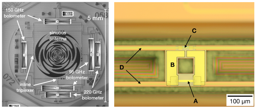
Except for the features on the bolometer island, the fabrication of this Al-Mn detector wafer at Argonne was similar to previous SPT-3G detectors, as detailed in Posada:2016. The layout of the SPT-3G pixel and the Al-Mn bolometer island are shown in Fig. 1. The TES films are 75 thick, sputtered from aluminum doped with 850 ppm manganese by atomic percentage, capped with 15 Ti and 15 Au. The 15 Au cap layer protects the TES film after deposition, and the 15 Ti layer prevents the formation of a compound between the Au cap and the Al in the TES film. The TES film was patterned using lift-off to define 10 by 70 devices. After TES film deposition, the wafer was baked at 180 C for 10 min to adjust the to the target of 420 . The Au cap is a normal metal, so it reduces through the proximity effect, but the change in is small because the Au layer is thin. A 600 palladium film was also deposited on the island, overlapping with the TES, to increase the total heat capacity and improve the electrothermal stability of the bolometer. This Pd film was thinner than the 850 films used previously in SPT-3G, in order to reduce the thermal time constant of the detectors.
3 Detector Performance
3.1 Electrothermal properties
The yield of functional detectors on the Al-Mn detector wafer is very similar to the rest of SPT-3G Bender:2018dwl; Bender:2019. Of 1572 wired detectors, 91.7% have nominal resistances measured at 300 and 89.9% correspond to measured resonances in the readout electronics. Losses are due to a combination of on-wafer opens and shorts, defects in wirebonding, and open channels in the multiplexing readout electronics (%). During routine observing during May 2019, an average of 79.4% of all detectors were actually operated in the transition. Nearly all of the additional losses (9.6% of the 10.4% difference) are due to a minimum requirement on optical responsivity.
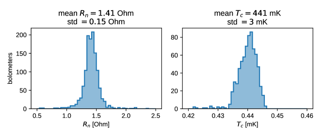
The TES and were measured in the lab prior to deployment on approximately one third of the detectors on the wafer. The measured of was acceptably close to the 420 target and had excellent uniformity of better than 1% across the wafer, as shown in Fig. 2. This difference in is typical of the batch-to-batch variation of devices fabricated at Argonne. The of each bolometer in the deployed system is estimated as
| (1) |
where is the total resistance measured by the readout system in the normal state, is the average parasitic impedance as a function of bolometer bias frequency111The parasitic impedance measured in the superconducting state is dominated by reactances that produce a characteristic frequency-dependence across all detector wafers and readout modules. , and is an empirical correction factor accounting for stray capacitance as a function of resonator index in the LC multiplexer chips as described in Dutcher:2018fod. An of was measured in the deployed wafer, also shown in Fig. 2. Of the variance in , 0.06 is attributable to using a model for rather than bolometer-by-bolometer measurements, and much of the remainder is likely due to residual calibration uncertainties in the readout electronics; DC four-wire measurements of typically show much lower scatter than measurements made with our frequency-domain multiplexing (fMux) readout electronics. The variance in in Fig. 2 should therefore not be interpreted as entirely due to physical variation in across the wafer.
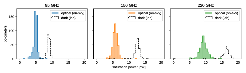
The saturation powers were measured both in the lab and with optical load in the field, shown in Fig. 3. The detectors are operated under a voltage bias by placing a shunt resistor in parallel with the TES. Saturation powers are calculated assuming that there is an additional 0.9 stray inductance in series with the shunt resistor. Although we do not have a complete model of all parasitic impedances in the readout circuit, we find that this value is similar to previous measurements of this stray inductance, and including this parasitic impedance alone is sufficient to eliminate the spurious dependence of the saturation power on bias frequency222Note that saturation powers reported in Dutcher:2018fod do not include this correction.. Since the saturation power depends on the thermal conductivity of the SiNx legs supporting the bolometer island, its value should be independent of the frequency at which it is biased by the readout electronics. Relative to the saturation powers measured using nominal values of components in the readout circuit, the saturation powers are increased by
| (2) |
where the saturation power assuming the nominal value of the shunt resistor, is the TES bias frequency, and is the inductance in series with the shunt resistor. The target saturation power for this wafer, as for previous SPT-3G detectors, is 10 / 15 / 20 for 95 / 150 / 220 . Operated at a base temperature of 280 , the median dark saturation powers were measured to be 10.6 / 14.8 / 19.1 , in excellent agreement with the target. During 2019 we began operating the SPT-3G receiver at a higher base temperature of 315 to improve the 3He/4He refrigerator cycle efficiency, so the saturation powers shown Fig. 3 are smaller but still have sufficient margin to avoid saturation.
3.2 Optical properties
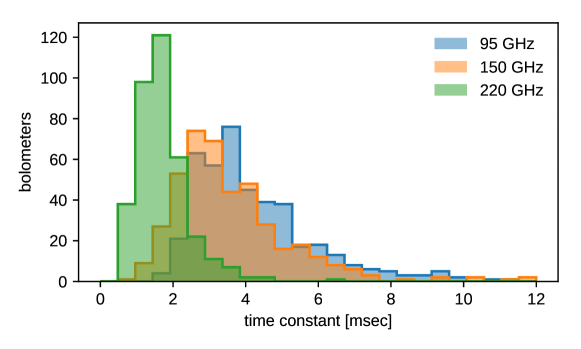
Optical time constants are measured regularly during observing using a chopped thermal source in the center of the SPT-3G secondary mirror. The median time constants by bolometer are shown in Fig. 4 and average 4.4 / 3.6 / 1.7 for 95 / 150 / 220 detectors, when measured with atmospheric loading at an elevation of 67.5 deg. The electrical power is highest for the 220 detectors, which results in the smaller optical time constants for this band. At the SPT-3G scan speed of 1 deg/sec on the azimuth bearing (less on the sky), the 3 frequencies of these TESs correspond to angular multipoles between 30,000 and 90,000 depending on observing elevation and band. Since the 3 point of telescope beam at 150 is , the detectors are fast enough to preserve good sensitivity to point sources.
To measure the optical efficiency, the detectors were illuminated by a blackbody source, and saturation powers were measured at eight temperatures of the blackbody between 8 and 15 . The measured saturation powers, , as a function of cold load temperature, , are fit to the model
| (3) | ||||
where the fit parameters and represent respectively the saturation power with no optical load and the optical efficiency. Several additional factors are included to correct for systematic biases in the measurement:
-
•
Wafer heating: The cold load aperture illuminates only one triangular hextant of the wafer, through three low-pass metal-mesh filters (cutoff of 300 ), and other detectors are blocked by an aluminum plate maintained at the base temperature near 250 . The saturation powers of blocked detectors show a small linear dependence on the cold load temperature, suggesting that the radiative load is heating up the wafer slightly. We fit data from each blocked detector to a linear model of the form , compute the average of the slopes across all bolometers in each observing band, and then assume that the illuminated bolometers experience the same thermal effects as the blocked detectors by including the term in Eq. 3. The net effect of this term is to decrease the estimated optical efficiency.
-
•
Filter transmission: The blackbody illuminates optically active detectors through a stack of three low-pass metal-mesh filters. While we do not have high-quality measurements of all filters over the full observing band, a measurement of one filter over the 150 and 220 bands has an average transmission of 96%. For simplicity, we therefore assume each filter has a fixed frequency-independent transmission of 96%, represented by the factor in Eq. 3.
-
•
Triplexer response: represents the frequency response of the inline triplexer for each band, which is taken from Sonnet simulations that assume a dielectric thickness typical of deployed wafers.
- •
-
•
Parasitic resistance in series with TES: As discussed in Section 3.1, there is an impedance in series with the TES, so that the voltage bias produced by the shunt resistor is divided between the series resistance and the TES. This effect is accounted for by the second factor in front of the integral in Eq. 3.
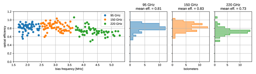
Fig. 5 shows the total optical efficiency as a function of bias frequency, estimated from the fit of Eq. 3. The mean efficiencies are 81% / 83% / 73% for 95 / 150 / 220 . The correction for the bias inductance has removed most of the spurious bias-frequency-dependence of optical efficiency within each band. Some slight dependence may remain in the 220 detectors, which could explain the lower estimate efficiency in that band.
In addition to the lab measurements, we also routinely measure the noise-equivalent temperature (NET) of the detectors during observing. While NET is not an equivalent metric to optical efficiency, poor optical efficiency will degrade the NET. The median NET during June 2019 for this Al-Mn wafer was 675 / 523 / 1919 for 95 / 150 / 220 detectors, versus 640 / 511 / 1815 for all other detectors. The small difference in NET between the Al-Mn wafer and the other Ti/Au SPT-3G wafers is comparable to the variation among the Ti/Au wafers, suggesting that overall performance and optical efficiency of the Al-Mn is similar to the Ti/Au.
4 Status and Outlook
We have fabricated an array of Al-Mn TES bolometers for the SPT-3G experiment. Extensive lab characterization of this array indicates that it meets our design specifications for normal resistance, saturation power, critical temperature, and optical efficiency, with high uniformity in all of these parameters. It was installed in the SPT-3G receiver and has been used in the 2019 observing season, where on-sky yield and NET are very similar to the other detector wafers. The excellent overall performance indicates that Al-Mn TES bolometers produced by Argonne would be suitable for a next-generation CMB experiment such as CMB-S4.