Projective Quasiparticle Interference of a Single Scatterer
to Analyze
the Electronic Band Structure of ZrSiS
Abstract
Quasiparticle interference (QPI) of the electronic states has been widely applied in scanning tunneling microscopy (STM) to analyze electronic band structure of materials. Single-defect-induced QPI reveals defect-dependent interaction between a single atomic defect and electronic states, which deserves special attention. Due to the weak signal of single-defect-induced QPI, the signal-to-noise ratio (SNR) is relatively low in a standard two-dimensional QPI measurement. In this paper, we introduce a projective quasiparticle interference (PQPI) method, in which a one-dimensional measurement is taken along high-symmetry directions centered on a specified defect. We apply the PQPI method to a topological nodal-line semimetal ZrSiS. We focus on two special types of atomic defects that scatter the surface and bulk electronic bands. With enhanced SNR in PQPI, the energy dispersions are clearly resolved along with high symmetry directions. We discuss the defect-dependent scattering of bulk bands with the non-symmorphic symmetry-enforced selection rules. Furthermore, an energy shift of the surface floating band is observed and a new branch of energy dispersion () is resolved. This PQPI method can be applied to other complex materials to explore defect-dependent interactions in the future.
I Introduction
In scanning tunneling microscopy (STM), quasiparticle interference (QPI) of electronic states has been a powerful tool to analyze the electronic band structure of condensed matter materials Crommie1993 ; Hasegawa93 ; LCDavis91 ; Avouris94 ; Petersen98 ; Sprunger1764 ; PhHofmann97 ; Pascual04 ; Weismann1190 ; Hoffman1148 ; Wang03 ; kostin2018imaging ; Aynajian2012 ; Allan2013 ; Roushan2009 ; ZhangTong09 ; Zeljkovic2014 ; Chang2016 ; Inoue1184 ; Zheng2016 ; Batabyale1600709 . QPI arises when the electronic state with initial momentum is elastically scattered to a final momentum . The potential barrier of scattering is often induced by point defects, steps or other local perturbations in materials. The scattering process leads to a spatial oscillation of electronic state with wave vector . The wave vector can be extracted from Fourier transform of QPI oscillations. As a function of energy E, the dispersion reflects the electronic band structure in -space.
The QPI study initially focused on electronic surface state, whose QPI oscillation (or Friedel oscillation) decays slowly with increasing distance from the scattering center Crommie1993 ; Hasegawa93 ; LCDavis91 ; Avouris94 . QPI has been thereafter applied in both surface states of materials, and electronic structure of two-dimensional (2D) materials Petersen98 ; Sprunger1764 ; PhHofmann97 ; Pascual04 . On the other hand, parallel features in Fermi surface structure may cause anisotropic propagation of a three-dimensional (3D) band, which can also result in a strong QPI oscillation on the sample surface Weismann1190 . The standard QPI measurement requires a 2D grid measurement, while in some special case it can be reduced to measurement due to a quasi electronic structure near an edge or homogeneous electronic structure induced by a single defect Haim2018am ; Liu_2017 ; Drozdov_2014 . The development of QPI technique enables extensive analysis of band structure of complex materials, including high- superconductors Hoffman1148 ; Wang03 ; kostin2018imaging , heavy fermion systems Aynajian2012 ; Allan2013 , and topological materials Roushan2009 ; ZhangTong09 ; Zeljkovic2014 ; Chang2016 ; Inoue1184 ; Zheng2016 ; Batabyale1600709 .
Although all QPI oscillations are related to the underlying electronic band structure, QPI induced by a single scatterer deserves special attention Inoue1184 ; Zheng2016 ; Simon2009 ; Derry2015 . Different types of point defects trigger defect-dependent interaction between the defect and electronic states. The QPI analysis around specified point defects can reveal a selective scattering. For example, in topological nodal-line materials ZrSiS and ZrSiSe xu2015two ; hu2016evidence ; schoop2016dirac , two different types of point defects are found to scatter electronic states of the floating surface band ZZ2018NatCom ; Surface_floating and bulk band, respectively lodge2017observation ; butler2017quasiparticle ; Bu2018PRB ; ZZ2018NatCom ; surface_termination . In ZrSiSe, both the surface and bulk bands were observed to be scattered by a single defect Bu2018PRB ; ZZ2018NatCom , which has not been detected yet in ZrSiS.
However, the QPI signal around a single scatterer is relatively weak, resulting in a low signal-to-noise ratio (SNR) in the Fourier-transformed QPI pattern. The vague band structure in this analysis limits the data-based discussion of physical properties. Here in this paper, a new type of point defect is discovered in ZrSiS, and a projective QPI (PQPI) method is introduced to analyze the scattered electronic bands in two different point defects, with a much higher SNR. The first new type of Zr-site defect scatters both the surface and bulk band. The second type S-site defect only scatters the bulk band, which has been observed before lodge2017observation with a different interpretation. A preliminary 2D QPI measurement shows that the QPI pattern induced by a single defect is anisotropic and highly concentrated along high symmetry directions. With the PQPI method, we could clearly resolve the dispersion branches and compare them with the density functional theory (DFT) calculation. We discuss the selective scattering with non-symmorphic symmetry-related selection rules. We also observe a possible defect-induced energy shift of the floating surface band, and an extra bulk band dispersion of branch. PQPI is a simple and intuitive method that can be applied in general single scatterer induced QPI studies of different materials.
II Experimental Method
Single crystals of ZrSiS were grown by a two-step chemical vapor transport method using iodine as a transport agent sankar2017crystal . In the first step, a stoichiometric amount of 99.9 % purity precursors of Zr:Si:S = 1:1:1 molar ratio was pressed into a tablet, and put in an alumina crucible. After sealed in an evacuated quartz ampoule, the sample was treated at 1100 ∘C for two days and then furnace-cooled to room temperature. In the second step, the tablet of ZrSiS was ground into a fine powder and then sealed in an evacuated quartz ampoule with 5mg/cm3 iodine. The quartz ampoule was treated in a two-zone tube furnace with a thermal gradient of about 1100 ∘C - 950 ∘C. After a period of 8 days, single crystals of ZrSiS were obtained.
STM measurements were carried out in a commercial ultra-high vacuum system Bu2018PRB ; zheng2017study ; FeiY_O_vacancy ; FeiY_Charge_order . An electrochemically etched tungsten tip was treated with field emission on a single crystalline of the Au (111) surface. The samples were cleaved in situ at liquid nitrogen temperature and immediately inserted into the STM head. A bias voltage was applied to the sample, and the tunneling current collected from the tip was maintained at a fixed setpoint by a feedback loop control. All data were acquired at liquid helium temperature ( 4.5 K). The differential conductance () spectrum was acquired with a standard lock-in technique with modulation of 10 mV at 1213.7 Hz. The integration time is 3 ms for a single spectrum in 2D measurement. In a grid measurement (2D or 1D), the tip was moved to a different grid point in constant current mode. At each grid point, the feedback was turned off while taking the corresponding spectrum. Afterward the feedback was turned on again, and the tip was moved to the next point for data collection. The DFT calculations were carried out using the Vienna simulation package (VASP) Kresse96efficient ; Kresse99paw ; Perdew96GGA ; Marzari97prb . A supercell with a vacuum layer larger than nm was applied in the slab model.
III Results and Discussion
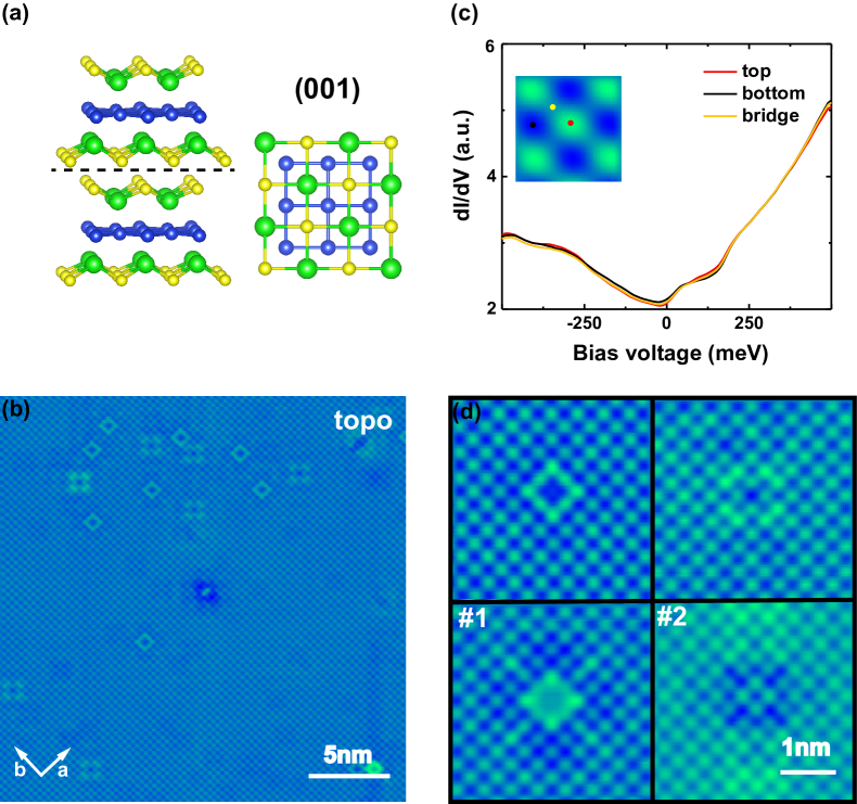
The family of ZrSiX (X S, Se, Te) shares a layered crystal structure. In Fig. 1(a), the crystal structure of ZrSiS shows that a square lattice of Si atoms is sandwiched between two sets of ZrS bilayers with glide mirror symmetry xu2015two ; Wang1995Main . Then the crystal structure of ZrSiS is non-symmorphic with Si lattice as the mirror plane. After an inversion towards the mirror plane and a glide of the plane with a vector of (where is the lattice constant of the ZrS bilayer), the crystal structure becomes the same as the original one. This non-symmorphic symmetry is critical to the topological properties of ZrSiS. For STM experiment, the single crystal sample is cleaved between two ZrS bilayers, with a S layer naturally exposed to be the surface plane. Figure 1(b) displays a typical topography taken on the exposed S surface, with a tunneling junction of mV and nA. In the topography, a clear square lattice can be observed with an interatomic spacing of Å. For the family of ZrSiX, the density of states (DOS) around the Fermi level is mainly contributed by electrons of Zr atoms xu2015two . Top sites of the square lattice are determined to be at locations of Zr atoms, even though Zr atoms are beneath the cleaved surface plane of S atoms.
Different from that in ZrSiSe Bu2018PRB , our ZrSiS experiment shows a bias-independent topography, without a shift of square lattice for different bias-voltage polarities. In a clean area of the sample (12 12 nm2), we performed a 2D spectrum measurement, with the topography acquired simultaneously. A supercell image was created by overlaying portions of the topography, following the algorithm in Ref. Lawler10nature ; Zeljkovic12NatMat . The supercell image is shown in the inset of Fig. 1(c), based on which the measured spectra are separately extracted over the top, hollow, and bridge sites. As shown in Fig. 1(c), the spectra at different sites are almost indistinguishable. They all exhibit a nonzero DOS around the Fermi level (zero bias), while the DOS of occupied state is smaller than that of the empty state. The spatially homogeneous spectrum is consistent with the bias-independent topography.
In Fig. 1(b), sparse point defects of different types can be observed within the square lattice. A typical diamond- and X-shaped defects are enlarged in the top row in Fig. 1(d), whose centers are at Zr and S sites, respectively. In previous STM studies of both ZrSiS and ZrSiSe lodge2017observation ; butler2017quasiparticle ; Bu2018PRB ; ZZ2018NatCom , the diamond (X-shaped) defects are found to selectively scatter the electronic surface band (bulk band). For ZrSiSe, a strong scatterer is found to scatter both the surface and bulk bands Bu2018PRB , which is hitherto not reported in ZrSrS. In the bottom row of Fig. 1(d), we show two different types of atomic point defects in ZrSiS, QPI around which is the main focus of this paper.
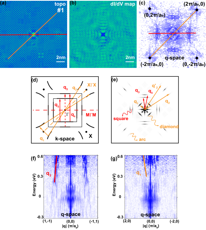
The bottom left defect in Fig. 1(d) is centered at the Zr site, around which a larger topography ( nm2 ) is shown in Fig. 2(a). To study QPI around a single atomic defect, a standard method is to obtain the maps from spectroscopy measurement. For a single map, a quick procedure is to collect the signal at the fixed bias voltage while scanning the tip in constant current mode. Along with the constant-current topography in Fig. 2(a), a map was taken simultaneously at mV. As shown in Fig. 2(b), this map exhibits an obvious pattern of standing wave centered around the point defect, referred as a QPI image later. The standing wave originates from the point-defect-induced scattering between electronic states of different wave vectors (initial and final ) but the same energy. In Fig. 2(b), the QPI image is not azimuthally symmetric but shows strong oscillations along the lattice direction and the diagonal () direction. Fourier transform of the map is calculated and drawn in Fig. 2(c). Similar to the previous report for ZrSiSe Bu2018PRB , the Fourier-transformed QPI pattern can be mainly partitioned into three groups: the central diamond, the concentric square, and four sets of parallel lines around Bragg peaks.
The QPI pattern is described in the momentum space with . Figure 2(d) shows a contour of constant energy (CCE) model similar to that in Ref. Bu2018PRB . For the floating surface band ZZ2018NatCom ; Surface_floating , there are four pairs of short parallel arcs around four X points. The scattering between parallel arcs in the same pair () corresponds to the central diamond in the QPI pattern. Scattering between short arcs in diagonal pairs () corresponds to the parallel lines around Bragg peaks in the QPI pattern shown in Fig. 2(e). For the bulk band, two concentric squares in the CCE model may contribute to concentric squares in the QPI pattern, with possible wave vectors , and . In the QPI pattern in Fig. 2(c), the scattering of both the surface band and bulk band can be identified, confirming the discovery of a new type of scatterer in ZrSiS. For the concentric squares in the QPI pattern, either a single square or two squares have been found for different point defects in ZrSiX lodge2017observation ; butler2017quasiparticle ; Bu2018PRB ; ZZ2018NatCom . The concentric square indicated by wave vector has never been found in literature and our experimental results. Without a high SNR in the QPI pattern, it is hard to judge whether the results are intrinsic characteristics of the point defect or just vague and indistinct signals with limited SNR. For simplicity, we intentionally forbid the scattering between outer to outer squares when calculating the -space map in Fig. 2(e).
To study the energy-dependent QPI pattern, a three-dimensional (3D) dataset has to be taken. For each spatial point in the scan area, the feedback loop is temporarily interrupted and a spectrum is taken in a selected voltage range, with the energy . After the measurement, the energy-dependent maps can be extracted from the 3D dataset for further analysis. A long time measurement is necessary for this process (e.g. 12-24 hours), in which the system instability and thermal-drift affect the SNR. To display the energy-dependent QPI result, the Fourier-transformed result is often shown along a high symmetry direction in space and plotted as a function of the energy. As shown in Fig. 2(f), the Fourier-transformed result is displayed along the high symmetry direction, from to in -space [red line in Fig. 2(c)]. The concentric square in the QPI pattern intersects with this line at the wave vector , later confirmed as . In Fig. 2(f), the energy-dependent dispersion of can be observed, as guided by the red solid line. Similarly, figure 2(g) shows the Fourier-transformed result along the orange line in Fig. 2(c), from one Bragg peak of to the diagonal Bragg peak of in -space. The diamond in the QPI pattern intersects with this line at , and the dispersion of can be observed in Fig. 2(g). We can observe a limited SNR in the energy-dependent results, which hinders a precise extraction of dispersions of and branches.
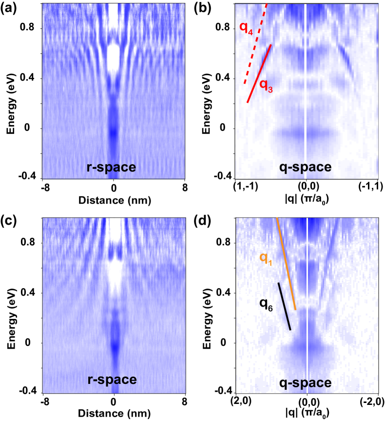
Here in this work, we introduce a simple and intuitive method, a projective quasiparticle interference (PQPI) on a single defect, to study the same energy-dependent scattering and extraction of the electronic band structure. In the two-dimensional QPI image [Fig. 2(a)], the standing wave propagates strongly along the lattice direction and the diagonal direction. In this PQPI method, the spectra were measured at dense spatial points along with two corresponding linecuts as labeled in Fig. 2(a). By decreasing dimension from 2D to 1D in real space measurement, we could increase the average number in the spectroscopy measurement. In the following 1D linecut measurement, each spectrum is acquired with the same parameters as in 2D measurement but averaged 5 times. The effect of system instability and thermal-drift is also lessened within the short measurement time (e.g. half an hour for a single linecut).
In Fig. 3(a), the measured spectrum is shown as a function of energy (each vertical line), along the linecut of diagonal direction. For each energy, the oscillating standing wave can be observed along the linecut in the real space. The real-space signal can be further Fourier-transformed, leading to the -space QPI pattern along the high symmetry direction from to . As shown in Fig. 3(b), the branch is more clearly identified, from the strongly enhanced SNR in the PQPI measurement. In the meantime, there is no clear dispersion signal of scatter wave vector (guided by a red dashed line) in Fig. 3(b). Because of the short measurement time in PQPI, the energy range is enlarged to meV with an energy resolution of meV. A similar spectroscopy measurement was taken along the lattice direction, with the real-space data shown in Fig. 3(c). The Fourier-transformed result in -space is shown in Fig. 3(d), in which the branch exhibits a clearly resolved dispersion (later confirmed by DFT calculations). With the relative high SNR, another branch is also identified, which will be discussed later. Putting Fig. 3(b) and 3(d) together, we conclude that this special impurity scatters both electronic surface and bulk band, similar to the special defect found in ZrSiSe Bu2018PRB . Only one branch is identified for the scattering within concentric squares.
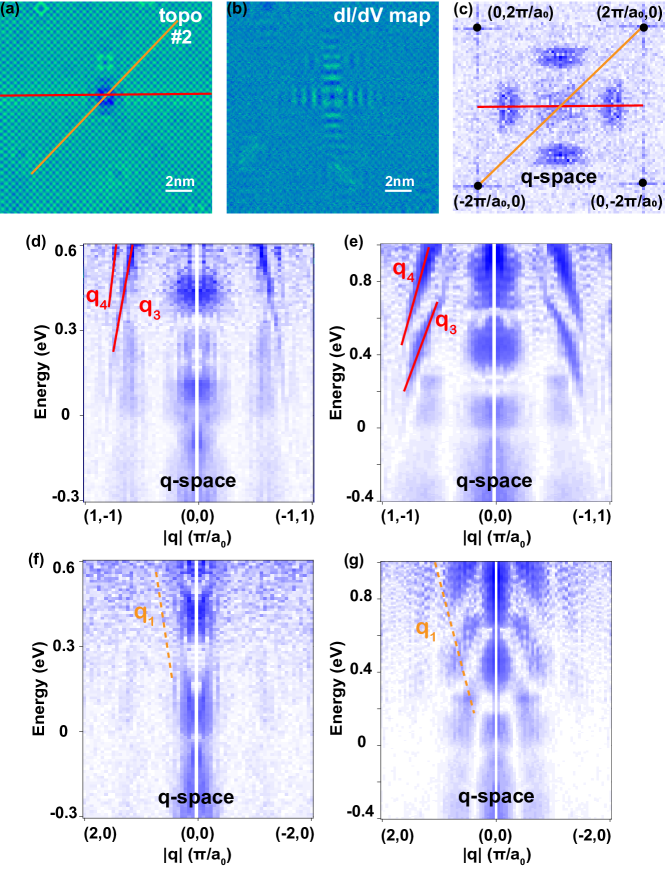
Now we turn to the second type point defect (). As shown in the bottom right image in Fig. 1(d), this type of defect is centered at the S site. A larger topography around this impurity was taken [Fig. 4(a)]. For the same field of view, the map at the bias voltage mV was also simultaneously taken. As shown in Fig. 4(b), the standing wave around this defect is observed to mainly propagate along the direction with respect to the lattice direction. With a nearby X-shaped defect, the QPI image of our interest is partially affected by the X-shaped-defect-induced standing wave. The map in Fig. 4(b) is Fourier transformed, leading to the QPI pattern in space in Fig. 4(c). The concentric squares appear in the center of the QPI pattern, while the diamond and four sets of parallel lines around Bragg peaks are absent. This defect seems only scatter the bulk band which is similar to the X-shaped defect. From the 3D spectroscopy dataset, figure 4(d) shows the extracted Fourier-transformed result along the -space red line in Fig. 4(c), as a function of energy. We could roughly distinguish two dispersed lines, labeled as and branches, respectively.
For the PQPI measurement, two real-space lines are chosen in Fig. 4(a) to be away from the extra standing wave from the X-shaped defect. The spectrum was measured along the line of diagonal direction, whose Fourier transform is performed and shown in Fig. 4(e). Within a large range of energy, two dispersed branches ( and ) can be clearly identified, confirming the two vague dispersions in Fig. 4(e). Similarly, a series of spectra were measured along the line of lattice direction, whose Fourier-transformed result is presented in Fig. 4(g). Different from the QPI pattern in Fig. 3, the branch of dispersion is obviously absent, consistent with that in Fig. 4(c) and 4(f). The high SNR result in Fig. 4(g) confirms that this defect does not scatter the electronic surface band.
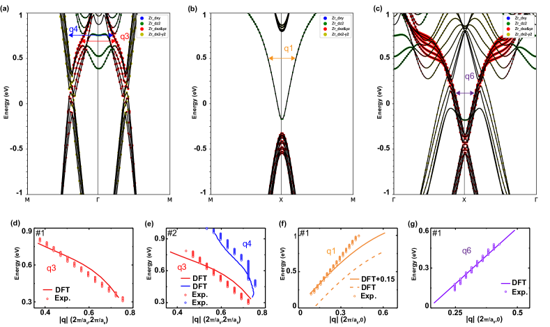
With the PQPI method, electronic branches from scattering can be clearly identified for different defects, which enables a precise extraction of dispersions and a quantitative analysis of the electronic band structure. For comparison, the electronic band structure of ZrSiS was calculated with a DFT of a slab model. Figure 5(a) shows the calculated band structure along the M--M direction in -space. The orbital projection has been considered in the band calculation, as presented with different colored dots in Fig. 5(a). From the DFT result, the bands near the Fermi surface are mainly contributed by different orbital components of Zr atoms. The outer band above the Fermi level with orange dots is mainly composed of components, meanwhile, the inner branch with red dots is composed of degenerated and components. The QPI branch with wave vector corresponds to the scattering between two internal bands originating from orbital of Zr atoms, or two sides of the internal square in the CCE model. The branch corresponds to the scattering between one band with orbital and another band with orbital of Zr atoms. In the CCE model, it is equivalent to the scattering from one side of the internal square to the opposite side of the outer square. The branch corresponds to the scattering between two bands with orbital of Zr atoms, which is indicated by a scattering between two sides of the outer square in the CCE model.
For the defect , we extract from the dispersed line with high intensity in Fig. 3(b). We made a constant energy shift of 100 meV for all the bands to present our DFT calculation results. With this constant shift, the extracted is well consistent with the calculated from the electronic band structure [Fig. 5(d)], which proves that the single branch in Fig. 3(b) matches with , instead of or . For the defect , we extract two dispersed branches in Fig. 4(e). In Fig. 5(e), the two extracted branches are well consistent with and calculated from the electronic band structure. With the decreasing energy, the amplitudes of and increase, but at different speeds. The dispersion of and merge around the energy of meV above the Fermi level, related with the nodal line in this nodal-line semimetal. The determination of the nodal line is consistent with the result for ZrSiSe in the previous work Bu2018PRB .
For these two defects, we discover either a single branch of scattering with wave vector or two branches of scattering with wave vectors and . This phenomenon is similar to that in previous reports for ZrSiS and ZrSiSe butler2017quasiparticle ; lodge2017observation ; surface_termination . The scattering of is never discovered heretofore. The high SNR in our results prove that the absence of scattering of is not due to a limited SNR in the QPI measurement, but an intrinsic property of the scattering. The appearance of a single branch () or two branches ( and ) are also clearly distinguished for two different point defects.
We next extract the scattering between electronic states in the surface band. Figure 5(b) shows the calculated band structure along the M--M direction, perpendicular to the two parallel arcs in the CCE model in -space. From the calculation, the branch happens between bands with orbital. This surface band is a floating band, originating from the surface-induced symmetry breaking from nonsymmorphic group to symmorphic wallpaper group . With the broken symmetry, the high band degeneracies are not protected anymore and can be lifted, resulting in floating or unpinned two-dimensional surface band Surface_floating . In Fig. 5(f), we extract from the dispersed line with high intensity in Fig. 3(d). The main dispersion of branch is linear from meV up to V. However, the calculated surface band has to be shifted meV up to match the experimental results, in addition to the constant energy shift for all bands. This energy shift of 150 meV may show the sensitivity of the floating band position with respect to the impurity surface_potential ; vacancy-induced . The deviation of the calculated surface band above meV may be related with a band bending effect in slab model calculation.
In Fig. 3(d), with the high SNR in our PQPI method, a new branch of can be observed, which has never been reported in previous STM experiments. The branch of is extracted and shown in Fig. 5(g). After careful comparison, this branch is found to be consistent with the scattering between bulk bands along direction [Fig. 5(c)]. Here the involved bulk bands bulk_band correspond to the corners of the inner concentric square in Fig. 2(d). Different from other branches, branch is related to a scattering process between adjacent Brillouin zone (BZ), as illustrated in the Supplementary Material spm . Normally the inter-BZ scattering is not detectable in QPI patterns. The glide mirror symmetry however effectively reduces the unit cell by half and expands the first BZ by two folds. Then the inter-BZ scattering of becomes an intra-BZ scattering in the non-symmorphic reshaped 1st BZ, which makes this scattering detectable. A similar picture has been applied to explain the anomalous half-missing Umklapp feature ZZ2018NatCom .
To explain the complicated defect-dependent scattering is very difficult. The clear scattering signal, however, enables analysis of symmetry-enforced selection rules stern2018prl . With preserved non-symmorphic symmetry for the bulk band, the band with and orbital can be characterized by an integer number of symmetry flavor and , respectively stern2018prl . The bands with different induce a direct band crossing and protected nodal-line (or Dirac ring) in ZrSiX. The bulk band scattering of branch happens between bands with orbital, with . The scattering of branch happens between bands with and orbital, with . Theoretically, the two branches must be distinguished by matrix elements because corresponds to scattering on the same and on different stern2018prl . For defect , only one branch is induced, which means that the orbital character of defect allows the scattering with , while forbids the scattering with . For defect , we see both and branches imply that the defect does not impose a selection rule, and the defect should have a mixed orbital character.
In the STM experiment, the tunneling current depends on the overlap between the tip and sample wavefunctions STM_book . The tip-related effect should also be discussed. The coexistence of and implies that the tip also does not impose a selection rule. The partial overlap between tip and sample wavefunctions is related to a nonuniversal value of , which is defined for the tip in Ref. stern2018prl . With a vertical -component, and orbitals of Zr atoms are prone to be overlapped with the typical s-wave symmetric tip state Spectral_decomposition . The overlap between orbital (in the plane) and the tip state is comparably smaller. Although with the same as the branch, the branch has never been observed. The minimum overlap between orbital and the tip state may lead to a negligible signal of in the QPI result. We emphasize that although the tip-related tunneling is involved in this detection of QPI, the observed phenomenon is robust against different samples and tips. For example, there are always two branches of scattering ( and ) for defect , detected by different tips on different samples. The type of defect is the key to induce selective scattering of electronic bands.
Although we cannot determine the different defect types yet, further exploration of the impurity spectrum may provide extra information for a later determination Zhou_impurity . The most frequently found defects are the diamond-shaped Zr-site defect and the X-shaped S-site defect, which are expected to be located within the top ZrS bilayer. When we measure the impurity spectrum for both defects, no obvious different features can be discerned when compared with the clean-area spectrum [see Fig. S2(a-b) in the Supplementary Material]. For the Zr-site defect , in contrast, the central impurity spectrum shows a peak feature around meV while the impurity spectrum at neighboring Zr site shows a peak feature around meV [see Fig. S2(c) in the Supplementary Material]. For the S-site defect , instead, the impurity spectrum at neighboring S site shows a peak feature around meV [see Fig. S2(d) in the Supplementary Material]. Although defect looks like a S-site defect, we cannot avoid the possibility that it is located at the Zr-site within the bottom ZrS bilayer. Please note that the neighboring dark S sites and the four radiating dark S lines share some similarities with that of bright Zr atoms in the topography of defect . In this possible situation, the Zr-site defects within the top bilayer are prone to scatter surface band, and the Zr-site defects within the bottom bilayer only scatter the bulk band. In the future, scanning transmission electron microscopy (STEM) may be applied to determine the defect types Bu_FeSe . A comprehensive theoretical model and first-principle calculations are also required to analyze the orbital character of different defects and explain the defect-dependent scattering and selection rules.
IV Summary
PQPI is a complementary tool to analyze the single-defect-induced QPI pattern and its energy dependence. With a single defect as the scattering center, the QPI oscillation decays with increasing distance away from the defect. A standard mapping of the QPI image is a measurement within a small area around the defect. Although a long time is required in the data-taking procedure, the SNR of the measurement is still relatively low. With an anisotropic propagation of the scattering oscillations, some high symmetry directions can be chosen in the PQPI method, along which a measurement can be finished within a short time. Changing from a measurement to a measurement, we can increase the data-taking time of every single spectrum and enhance the SNR of measured results.
In summary, we investigate single-defect-induced QPI oscillations in the nodal-line semimetal ZrSiS. A new type of Zr-site defect is found to scatter both the bulk band and surface floating band. With the PQPI method, clear QPI dispersions along high symmetry directions have been clearly resolved. The clear scattering signal enables a discussion about the non-symmorphic-symmetry-enforced selection rules. An extra energy shift of the surface floating band is determined and a new branch of scattering is discovered. The PQPI method can be generally applied in other complex materials to explore the distinct interaction between a single atomic defect and electronic states.
Acknowledgements.
We acknowledge and thank R. Queiroz, Z. Fang, X. Dai and H. Weng for discussions and communications. This work was supported by the National Basic Research Program of China (2019YFA0308602, 2016YFA0300402), the National Natural Science Foundation of China (NSFC-11374260, 11374261), and the Fundamental Research Funds for the Central Universities in China.References
- (1) M. F. Crommie, C. P. Lutz, and D. M. Eigler, Nature (London) 363, 524 (1993).
- (2) Y. Hasegawa and P. Avouris, Phys. Rev. Lett. 71, 1071 (1993).
- (3) L. C. Davis, M. P. Everson, R. C. Jaklevic, and W. Shen, Phys. Rev. B 43, 3821 (1991).
- (4) P. Avouris, I. Lyo, R. E. Walkup, and Y. Hasegawa, J. Vac. Sci. Technol. B: Microelectron. Nanometer Struct. Process. Meas. Phenom. 12, 1447 (1994).
- (5) L. Petersen, P. T. Sprunger, P. Hofmann, E. Lægsgaard, B. G. Briner, M. Doering, H. P. Rust, A. M. Bradshaw, F. Besenbacher, and E. W. Plummer, Phys. Rev. B 57, R6858 (1998).
- (6) P. T. Sprunger, L. Petersen, E. W. Plummer, E. Lægsgaard, and F. Besenbacher, Science 275, 1764 (1997).
- (7) P. Hofmann, B. G. Briner, M. Doering, H. P. Rust, E. W. Plummer, and A. M. Bradshaw, Phys. Rev. Lett. 79, 265 (1997).
- (8) J. I. Pascual, G. Bihlmayer, Y. M. Koroteev, H. P. Rust, G. Ceballos, M. Hansmann, K. Horn, E. V. Chulkov, S. Blügel, P. M. Echenique, and P. Hofmann, Phys. Rev. Lett. 93, 196802 (2004).
- (9) A. Weismann, M. Wenderoth, S. Lounis, P. Zahn, N. Quaas, R. G. Ulbrich, P. H. Dederichs, and S. Blügel, Science 323, 1190 (2009).
- (10) J. E. Hoffman, K. McElroy, D. H. Lee, K. M. Lang, H. Eisaki, S. Uchida, and J. C. Davis, Science 297, 1148 (2002).
- (11) Q. H. Wang and D. H. Lee, Phys. Rev. B 67, 020511 (2003).
- (12) A. Kostin, P. O. Sprau, A. Kreisel, Y. X. Chong, A. E. Böhmer, P. C. Caneld, P. J. Hirschfeld, B. M. Andersen, and J. C. Davis, Nat. Mater. 17, 869 (2018).
- (13) P. Aynajian, E. H. da Silva Neto, A. Gyenis, R. E. Baumbach, J. D. Thompson, Z. Fisk, E. D. Bauer, and A. Yazdani, Nature (London) 486, 201 (2012).
- (14) M. P. Allan, F. Massee, D. K. Morr, J. Van Dyke, A. W. Rost, A. P. Mackenzie, C. Petrovic, and J. C. Davis, Nat. Phys. 9, 468 (2013).
- (15) P. Roushan, J. Seo, C. V. Parker, Y. S. Hor, D. Hsieh, D. Qian, A. Richardella, M. Z. Hasan, R. J. Cava, and A. Yazdani, Nature (London) 460, 1106 (2009).
- (16) T. Zhang, P. Cheng, X. Chen, J. F. Jia, X. Ma, K. He, L. Wang, H. Zhang, X. Dai, Z. Fang, X. Xie, and Q. K. Xue, Phys. Rev. Lett. 103, 266803 (2009).
- (17) I. Zeljkovic, Y. Okada, C. Y. Huang, R. Sankar, D. Walkup, W. Zhou, M. Serbyn, F. Chou, W. F. Tsai, H. Lin, A. Bansil, L. Fu, M. Z. Hasan, and V. Madhavan, Nat. Phys. 10, 572 (2014).
- (18) G. Chang, S. Y. Xu, H. Zheng, C. C. Lee, S. M. Huang, I. Belopolski, D. S. Sanchez, G. Bian, N. Alidoust, T. R. Chang, C. H. Hsu, H. T. Jeng, A. Bansil, H. Lin, and M. Z. Hasan, Phys. Rev. Lett. 116, 066601 (2016).
- (19) H. Inoue, A. Gyenis, Z.Wang, J. Li, S. W. Oh, S. Jiang, N. Ni, B. A. Bernevig, and A. Yazdani, Science 351, 1184 (2016).
- (20) H. Zheng, S. Y. Xu, G. Bian, C. Guo, G. Chang, D. S. Sanchez, I. Belopolski, C. C. Lee, S. M. Huang, X. Zhang, R. Sankar, N. Alidoust, T. R. Chang, F. Wu, T. Neupert, F. Chou, H. T. Jeng, N. Yao, A. Bansil, S. Jia, H. Lin, and M. Z. Hasan, ACS Nano 10, 1378 (2016).
- (21) R. Batabyal, N. Morali, N. Avraham, Y. Sun, M. Schmidt, C. Felser, A. Stern, B. Yan, and H. Beidenkopf, Sci. Adv. 2, e1600709 (2016).
- (22) N. Avraham, J. Reiner, A. Kumar-Nayak, N. Morali, R. Batabyal, B. Yan, and H. Beidenkopf Adv. Mater. 30, 1707628 (2018).
- (23) X. G. Liu, H. J. Du, J. F. Wang, M. Y. Tian, X. Sun, and B. Wang, J. Phys.: Condens. Matter, 29, 185002 (2017).
- (24) Ilya K. Drozdov, A. Alexandradinata, Sangjun Jeon, S. Nadj-Perge, H. W. Ji, R. J. Cava, B. A. Bernevig, and A. Yazdani, Nat. Phys. 10, 664 (2014).
- (25) L. Simon, C. Bena, F. Vonau, D. Aubel, H. Nasrallah, M. Habar, and J. C. Peruchetti, Eur. Phys. J. B 69, 351 (2009).
- (26) P. G. Derry, A. K. Mitchell, and D. E. Logan, Phys. Rev. B 92, 035126 (2015).
- (27) Q. Xu, Z. Song, S. Nie, H. Weng, Z. Fang, and X. Dai, Phys. Rev. B 92, 205310 (2015).
- (28) J. Hu, Z. Tang, J. Liu, X. Liu, Y. Zhu, D. Graf, K. Myhro, S. Tran, C. N. Lau, J. Wei, and Z. Mao, Phys. Rev. Lett. 117, 016602 (2016).
- (29) L. M. Schoop, M. N. Ali, C. Straßer, A. Topp, A. Varykhalov, D. Marchenko, V. Duppel, S. S. P. Parkin, B. V. Lotsch, and C. R. Ast, Nat. Commun. 7, 11696 (2016).
- (30) A. Topp, R. Queiroz, A. Grüneis, L. Müchler, A. W. Rost, A. Varykhalov, D. Marchenko, M. Krivenkov, F. Rodolakis, J. L. McChesney, B. V. Lotsch, L. M. Schoop, and C. R. Ast, Phys. Rev. X 7, 041073 (2017).
- (31) Z. Zhu, T. R. Chang, C. Y. Huang, H. Pan, X. A. Nie, X. Z. Wang, Z. T. Jin, S. Y. Xu, S. M. Huang, D. D. Guan, S. Wang, Y. Y. Li, C. Liu, D. Qian, W. Ku, F. Song, H. Lin, H. Zheng, and J. F. Jia, Nat. Commun. 9, 4153 (2018).
- (32) K. Bu, Y. Fei, W. Zhang, Y. Zheng, J. Wu, F. Chen, X. Luo, Y. Sun, Q. Xu, X. Dai, and Y. Yin, Phys. Rev. B 98, 115127 (2018).
- (33) M. S. Lodge, G. Chang, C. Y. Huang, B. Singh, J. Hellerstedt, M. T. Edmonds, D. Kaczorowski, M. M. Hosen, M. Neupane, H. Lin, M. S. Fuhrer, B. Weber, and M. Ishigami, Nano. Lett. 17, 7213 (2017).
- (34) C. J. Butler, Y. M. Wu, C. R. Hsing, Y. Tseng, R. Sankar, C. M. Wei, F. C. Chou, and M. T. Lin, Phys. Rev. B 96, 195125 (2017).
- (35) C. C. Su, C. S. Li, T. C. Wang, S. Y. Guan, R. Sankar, F. Chou, C. S. Chang, W. L. Lee, G. Y. Guo, and T. M. Chuang, New J. Phys. 20, 103025 (2018).
- (36) R. Sankar, G. Peramaiyan, I. P. Muthuselvam, C. J. Butler, K. Dimitri, M. Neupane, G. N. Rao, M. T. Lin, and F. C. Chou, Sci. Rep. 7, 40603 (2017).
- (37) Y. Zheng, Y. Fei, K. Bu, W. Zhang, Y. Ding, X. Zhou, J. E. Hoffman, and Y. Yin, Sci. Rep. 7, 8059 (2017).
- (38) Y. Fei, K. L. Bu, W. H. Zhang, Y. Zheng, X. Sun, Y. Ding, X. J. Zhou, and Y. Yin, Sci. China Phys. Mech. Astron. 61, 127404 (2018).
- (39) Y. Fei, Y. Zheng, K. L. Bu, W. H. Zhang, Y. Ding, X. J. Zhou, and Y. Yin, Sci. China Phys. Mech. Astron. 63, 227411 (2020).
- (40) G. Kresse and J. Furthmüller, Phys. Rev. B 54, 11169 (1996).
- (41) G. Kresse and D. Joubert, Phys. Rev. B 59, 1758 (1999).
- (42) J. P. Perdew, K. Burke, and M. Ernzerhof, Phys. Rev. Lett. 77, 3865 (1996).
- (43) N. Marzari and D. Vanderbilt, Phys. Rev. B 56, 12847 (1997).
- (44) C. Wang and T. Hughbanks, Inorg. Chem. 34, 5524 (1995).
- (45) M. J. Lawler, K. Fujita, Jhinhwan Lee, A. R. Schmidt, Y. Kohsaka, Chung Koo Kim, H. Eisaki, S. Uchida, J. C. Davis, J. P. Sethna, and Eun-Ah Kim Nature (London) 466, 347 (2010).
- (46) I. Zeljkovic, E. J. Main, T. L. Williams, M. C. Boyer, K. Chatterjee, W. D. Wise, Y. Yin, M. Zech, A. Pivonka, T. Kondo, T. Takeuchi, H. Ikuta, J. Wen, Z. Xu, G. D. Gu, E. W. Hudson, and J. E. Hoffman, Nat. Mater. 11, 585 (2012).
- (47) C. Mann, D. West, I. Miotkowski, Y. P. Chen, S. Zhang, and C. K. Shih, Nat. Commun. 4, 2277 (2013).
- (48) T. Förster, P. Krüger, and M. Rohlfing, Phys. Rev. B 91, 035313 (2015).
- (49) B. B. Fu, C. J. Yi, T. T. Zhang, M. Caputo, J. Z. Ma, X. Gao, B. Q. Lv, L. Y. Kong, Y. B. Huang, P. Richard, M. Shi, V. N. Strocov, C. Fang, H. M. Weng, Y. G. Shi, T. Qian, and H. Ding, Sci. Adv. 5, eaau6459 (2019).
- (50) See Supplementary Material at http://
- (51) R. Queiroz, and A. Stern, Phys. Rev. Lett. 121, 176401 (2018).
- (52) C. J. Chen, Introduction to Scanning Tunneling Microscopy (Oxford University Press, 1993).
- (53) J. Nieminen, I. Suominen, R. S. Markiewicz, H. Lin, and A. Bansil, Phys. Rev. B 80, 134509 (2009).
- (54) T. Zhou, W. Chen, Y. Gao and Z. D. Wang Phys. Rev. B 100, 205119 (2019).
- (55) K. L. Bu, B. Wang, W. H. Zhang, Y. Fei, Y. Zheng, F. Z. Ai, Z. X. Wu, Q. S. Wang, H. L. Wo, J. Zhao, C. H. Jin and Y. Yin, Phys. Rev. B 100, 155127 (2019).