Interplay of Dirac nodes and Volkov-Pankratov surface states in compressively strained HgTe
Abstract
Abstract inline
pacs:
72.25.Dc, 72.25.Hg, 81.05.DzPreceded by the discovery of topological insulators, Dirac and Weyl semimetals have become a pivotal direction of research in contemporary condensed matter physics. While easily accessible from a theoretical viewpoint, these topological semimetals pose a serious challenge in terms of experimental synthesis and analysis to allow for their unambiguous identification. In this work, we report on detailed transport experiments on compressively strained HgTe. Due to the superior sample quality in comparison to other topological semimetallic materials, this enables us to resolve the interplay of topological surface states and semimetallic bulk states to an unprecedented degree of precision and complexity. As our gate design allows us to precisely tune the Fermi level at the Weyl and Dirac points, we identify a magnetotransport regime dominated by Weyl/Dirac bulk state conduction for small carrier densities and by topological surface state conduction for larger carrier densities. As such, similar to topological insulators, HgTe provides the archetypical reference for the experimental investigation of topological semimetals.
The discovery of topological insulators has inspired a remarkably broad interest in materials whose band structures exhibit relativistic properties. The effects of a linear dispersion in one-dimensional edge channels of quantum spin Hall insulators König et al. (2007), as well as in two-dimensional surface states of three-dimensional topological insulators Hsieh et al. (2008); Brüne et al. (2011), have already been extensively studied. The implications of a linear band dispersion in three-dimensional conductors, however, have only recently begun to be explored. Such materials, dubbed Dirac or Weyl semimetals, represent a condensed matter realization of the Weyl/Dirac equations, and may provide an environment for studying the properties of quasiparticles which have been postulated, but not yet unambiguously demonstrated, to exist in nature.
In many of these materials Armitage et al. (2018), the Weyl or Dirac band crossing is caused by a band inversion, and is intimately connected to the point group symmetry of the crystal lattice. This lends similarities to the prototypical setup of topological insulators. In fact, both in the alkali pnictide (AB3, where A=(Na,K,Rb), B=(As,Sb,Bi)) and Cd2As3 families that boast a number of important Weyl/Dirac compounds, the inversion occurs between metallic -like and chalcogenic -like orbitals, a situation very similar to that found in HgTe. The correspondence in terms of band structure between these compounds and HgTe has indeed been known since the 1970s Jay-Guerin et al. (1977). The common motif is that, for the alkali pnictides and Cd2As3, the -like bands ( in the point group) cross and yield Dirac (or Weyl) points, while in HgTe the bands just touch, derives from the higher (zincblende) point group symmetry of the HgTe crystal. Small crystal distortions from the zincblende symmetry, as present in Weyl/Dirac semimetals, are sufficient to crucially modify the electronic structure at low energies.
In the 1980s, Volkov and Pankratov Volkov and Pankratov (1985) studied the interface between two semiconductor materials with mutually inverted bands, and reported a resulting band structure as depicted in Fig. 1a. It includes linear dispersing massless surface states -the states that are now interpreted as the defining property of topological insulators, and topologically trivial massive surface states. While the latter are currently commonly referred to as massive Volkov-Pankratov states (Tchoumakov et al., 2017), the former are often called topological surface states. Here, we use the historically accurate nomenclature of referring to both types of states identified in Ref. Volkov and Pankratov (1985) as Volkov-Pankratov states, and differentiating between them by qualifying them as either massless or massive. A generic Yang and Nagaosa (2014); Yi et al. (2014) even though experimentally often overlooked or neglected implication of bulk band inversion in Dirac or Weyl materials is the concomitant creation of these same Volkov-Pankratov states at energies even significantly away from the bulk crossing point. As such, while the bulk band structure of these systems exhibits a three-dimensional linear dispersion relation, massless Volkov-Pankratov states continue to support two-dimensional linearly dispersive bands as well. Thus, two and three-dimensional conducting states co-exist, and care must be taken in transport experiments to unambiguously assign any feature observed in the conduction profile of the sample to its individual origin.
As an additional challenge for the experimental analysis, Weyl and Dirac materials typically have a high carrier density - as a consequence, they are difficult or sometimes even impossible to gate. Moreover, because proper lithographic methods and thin layer approaches have yet to be developed, primitive contacting (such as needles and conducting glues) and patterning methods are usually employed, giving rise to many potential measurement artifacts resulting from inhomogeneous current distribution, which becomes even further enhanced by the application of magnetic fields. Such effects, sometimes summarized by the expression current jetting Arnold et al. (2016); Yoshida (1980); Reis et al. (2016) are, for instance, known to lead to inaccurate mobility measurements. Altogether, such concerns have cast significant doubt on the reliability of many of the early experiments on Dirac and Weyl materials Armitage et al. (2018).
The synoptic view of the beforementioned observations strongly suggests that materials of higher quality and more mature synthesis procedures are indispensable to truly discover the enigmatic Dirac and Weyl semimetallic state. In this paper, we report that compressively strained HgTe is an ideal choice for such an undertaking. It can be grown with high crystalline quality by molecular beam epitaxy (MBE), leading to exceptionally low inherent carrier densities. Furthermore, we can use well established lithographic techniques to precisely define a Hall-bar structure with low resistance alloyed ohmic contacts as well as electrostatic gate electrodes. These good contacts and exact device geometries ensure a well-defined homogeneous current distribution. Most importantly, the low intrinsic doping, together with the inclusion of a gate, allows us to controllably adjust the level of the Fermi energy via the carrier density within the band structure, tuning the conductance properties between surface state and bulk Dirac/Weyl node dominated transport. This allows us to confidently attribute transport characteristics to either their bulk or surface origin.
The low energy dispersion of HgTe is given by two quadratically dispersing -bands. For unstrained bulk HgTe, these bands are degenerate at the -point, as sketched in Fig. 1b. Under tensile strain, this degeneracy is lifted Liu and Leung (1975) due to lowering of the point group symmetry, and a topological bulk gap opens Brüne et al. (2011, 2014). The remaining surface conduction stems from the massless Volkov-Pankratov states implied by inversion of the -bands with the band, the latter of which, for the unstrained case, is located deep below the Fermi level at .
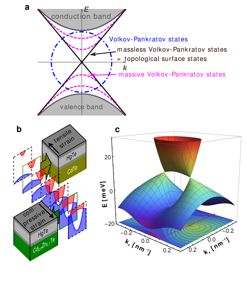
Under compressive strain, the degeneracy is likewise lifted, now with the two -bands shifting in opposite direction as for tensile strain. This leads to the formation of linear crossing points in the band structure. The in-plane compressive and tensile strain dependence of the bands around is visualized in Fig 1b, where the red domain highlights the conduction and the blue domain the valence regime. Experimentally, the tensiley strained 3D TI phase is accomplished by growth on a CdTe substrate (Fig. 1b). While there is no commercially available substrate with a lattice constant slightly below that of HgTe, compressive strain is experimentally still accessible through a superlattice virtual substrate Leubner et al. (2016) as sketched in Fig. 1b. The linear crossing points are further demonstrated in Fig. 1c via a band structure plot along the - plane in momentum space. It is the result of a 6-band kp calculation of the low energy band structure for the compressively strained case, where the axis denotes the layer growth direction and the axes the in-plane coordinates.
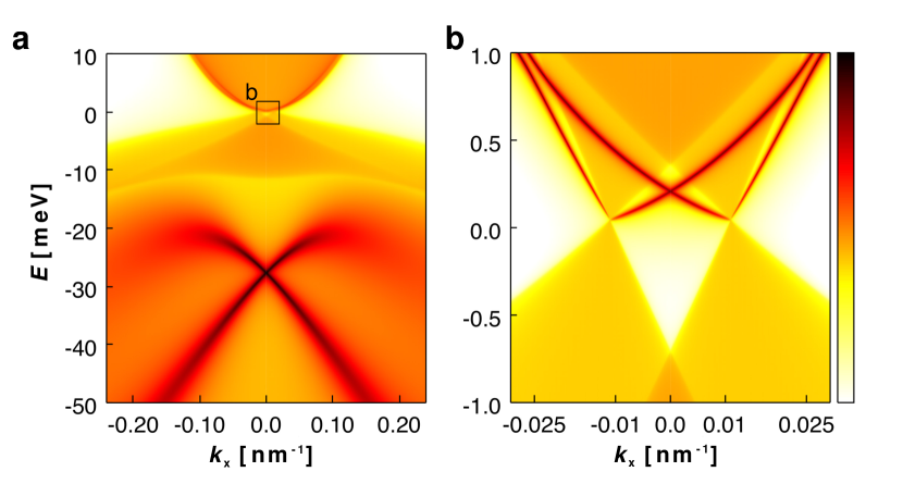
More information on the relation between bulk Dirac nodes and the inversion-induced surface states can be obtained from DFT calculations on a semi-infinite thick slab with a tellurium terminated interface to vacuum of compressively strained HgTe at a realistic value of the in-plane strain (see also supplementary information See Supplemental Material at xxx. ). Fig. 2a shows the calculated slab dispersion for an extended energy range centered around the Fermi level, exhibiting sharp dispersive surface features 20 meV below and right above the Fermi level, which is related to the inversion of the and bands. The breaking of spatial inversion symmetry in the zincblende structure splits each Dirac node into four Weyl points Ruan et al. (2016). For HgTe, Weyl points of opposite chirality project pairwise onto the (001) surfaces connected by inversion. Starting from two Dirac nodes in the unstrained zincblende structure, this yields four Weyl points per surface, with a Berry flux monopole charge of . Fig. 2b highlights the low-energy dispersion for the two surface-projected Weyl points of chirality +2. Weyl points of opposite chirality are connected by a Fermi arc Wan et al. (2011). The separation in momentum space between the Weyl nodes is estimated to be nm-1. As a consequence, zero-field experiments do not offer sufficient resolution to resolve the small energy and momentum scales at hand. As such, we hereafter consider all bulk transport in this sample to be described by Dirac physics and thus will refer to the energy of the crossing points as the bulk Dirac node. From this perspective, the band structure of compressively strained HgTe is virtually identical to that of typical 3D Dirac semimetals such as Cd3As2.
We report experimental results on a thick, compressively strained HgTe layer, grown on a virtual substrate consisting of a CdTe/ZnTe multilayer produced by a combination of MBE and atomic layer epitaxy (ALE) on a Si-doped GaAs substrate Leubner et al. (2016). This CdTe/ZnTe multilayer has a lattice constant between that of CdTe and ZnTe, and can be exactly tuned by setting the Cd/Zn ratio. In the present case, a lattice constant of is used to impose a compressive strain of on the HgTe layer (for details see the supplementary information See Supplemental Material at xxx. ). To increase sample quality and carrier mobility, two thick protective layers of are grown below and on top of the HgTe layer.
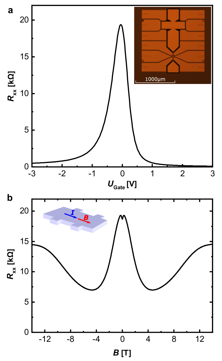
We pattern the sample using our standard Hall bar mask and optical lithography process into devices such as the one showed in the inset of Fig. 3. The mask contains two sizes of Hall bars, a larger one with a mesa having a width of and a separation of the longitudinal voltage leads of , and a smaller one with a width of and a contact separation of . The HgTe mesa’s are covered with a thick insulator followed by a thick Au gate electrode on top of a Ti sticking layer. Contacts are fabricated by first using a short dry etching step to provide a clean oxide-free surface for contacting, followed by in situ electron beam evaporation of AuGe and Au. Two separate devices, each containing Hall bars of both sizes were investigated in this study, all yielding consistent results with no substantial discrepancy between either the different devices or sample sizes. All measurements are carried out using standard low-noise and low-frequency AC techniques, and unless otherwise noted, are done at .
We first confirm that we can indeed efficiently adjust the carrier density in our sample as demonstrated by the influence of the gate voltage on the zero field longitudinal resistance shown in Fig. 3a. The longitudinal resistance changes by three orders of magnitude, from around to . The associated gate induced change of carrier density in the sample is determined by standard Hall measurements. We find that the density can be tuned from (p-type) for up to (n-type) for . The maximum of coincides with the lowest total density as well as with the change in the carrier type from electron to primarily hole transport. From this observation we infer that we can precisely tune the Fermi energy to the bulk Dirac node. Given that our Hall bars consist of 3 squares, the maximum corresponds to a sheet resistivity value of approximately , and thus of the order of magnitude expected for a diffusive Dirac system.Sbierski et al. (2014)
Tuning to minimal carrier density, and consequently moving the Fermi energy to the bulk Dirac node level, the longitudinal resistance versus a magnetic field applied parallel to the current is shown in Fig. 3b. A significant dip is observed as a function of , corresponding to a reduction of up to of the value of at . Such a negative magnetoresistance contribution is a defining feature implied by the chiral anomaly. Originally conceived as a symmetry violation in quantum field theory in comparison to its classical analogue, the chiral anomaly was first discussed in the context of solid-state systems by Nielsen et. al. Nielsen and Ninomiya (1983). There, the emergence of a chiral charge, i.e., an imbalance between left- and right moving Dirac particles, is naturally interpreted to be implied by an external field, as both particle branches are not independent, but connected through the crystal band structure. Weyl nodes (and magnetic field-split Dirac nodes) can act as magnetic monopoles in momentum space due to their Berry curvature, with a magnetic charge given by the chirality Hosur and Qi (2013). A magnetic field parallel to the driving electric field causes a pair of Weyl nodes with different chirality to shift in energy with respect to each other, causing a redistribution of carriers among the nodes. This increases the longitudinal conductivity upon increasing magnetic field strength. A Boltzmann equation calculation yields Son and Spivak (2013); Burkov (2015).
Experimentally, the negative magnetoresistance due to the chiral anomaly contribution is, for certain ranges of magnetic field, often overshadowed by other effects. For small magnetic fields , a minor increase of is observed, which we attribute to weak anti-localization based on its field and temperature dependence Lu and Shen (2015); Zhang et al. (2016). For large magnetic fields (above T), the chiral anomaly contribution becomes overcompensated to yield a total increase of longitudinal resistance, possibly due to impurity-imposed classical mechanisms of magnetotransport O’Handley (2000).
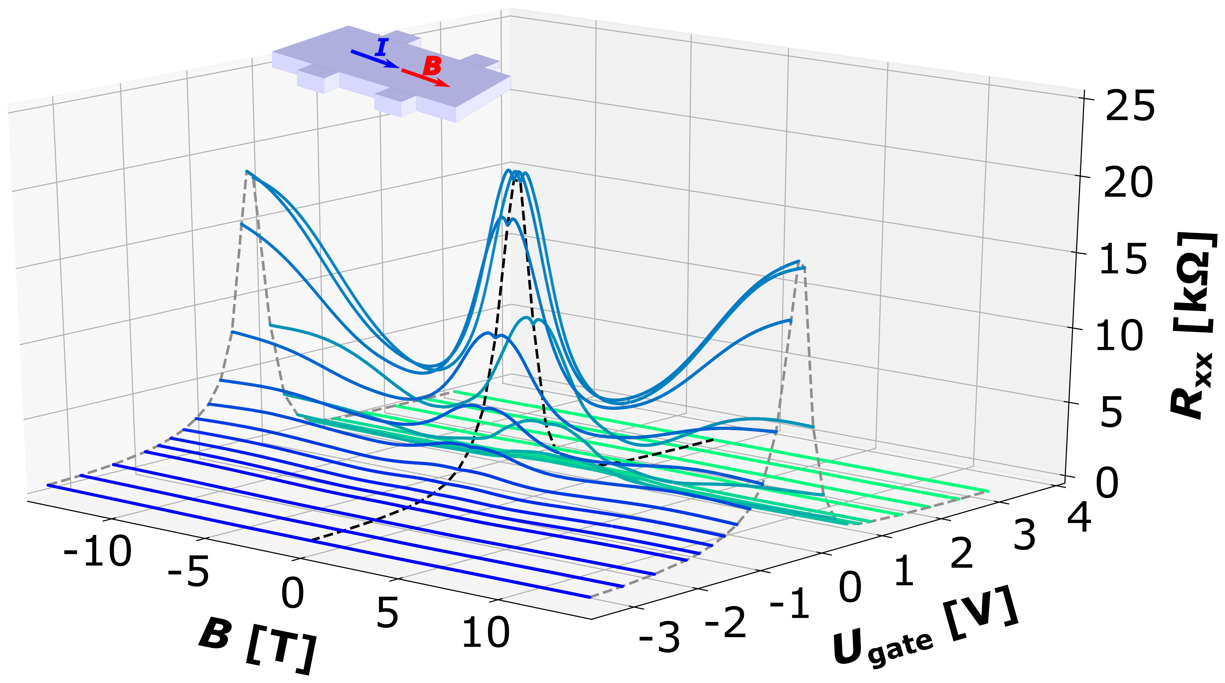
Strong evidence connecting the negative magnetoresistance phenomenon in Fig. 3b to the bulk Dirac nodes in the HgTe band structure derives from the gate voltage dependence of the magnetoresistance data, as presented in Fig. 4. The data of Figs. 3a and 3b are included as the line and dashed black lines, respectively. The visualization unambiguously demonstrates that the negative magnetoresistance is strongest, both in absolute numbers and percentage-wise, at , corresponding to a Fermi energy close to the bulk Dirac nodes. When the carrier density is increased, the longitudinal resistance at zero field, as well as the magnitude of the negative magnetoresistance, reduce quickly in magnitude. The reduction of the negative magnetoresistance phenomenon with high absolute gate voltage is equivalently observed for both positive (electron transport) and negative (hole transport). A slight asymmetry in the negative magnetoresistance decay for positive versus negative gate voltages can be attributed to an asymmetry in the electron and hole mobilities.
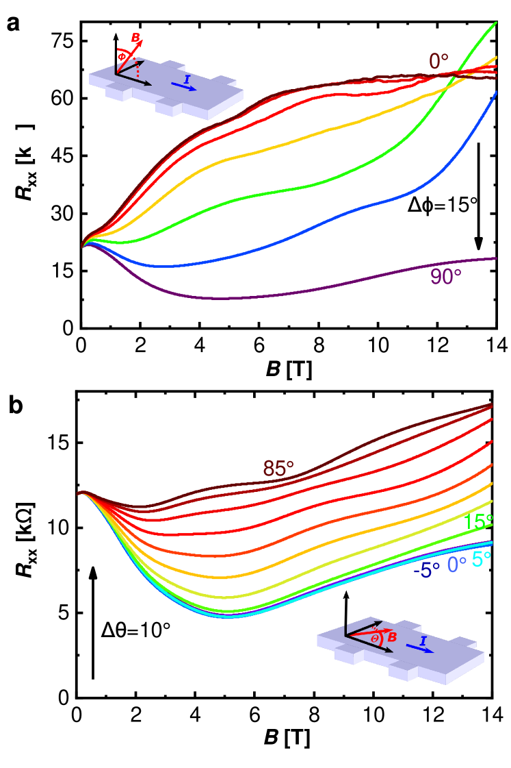
A further prototypical feature of the chiral anomaly is the implied angular dependence on the magnetic field , as only the magnetic field component parallel to the driving electric field produces an additional current. The angle dependence for is presented in Fig. 5. In Fig. 5a the magnetic field is rotated along the polar angle with for normal to the plane, and corresponding to . Fig. 5b shows the dependence of under variation of the azimuthal angle (in the sample plane). The magnetic field direction is varied from , representing , to nearly for .
While at higher fields, beyond which the chiral anomaly contribution has saturated, classical positive magnetoresistance contributions take over, both parts of Fig. 5 show that the amplitude of the negative magnetoresistance depends only on the component of along the current direction, as expected for the chiral anomaly. To further confirm the origin of the negative magnetoresistance, a control experiment, on an otherwise identical sample, but with a tensiley strained HgTe layer having a topological insulator band structure, was performed. In that case, only positive magnetoresistance contributions are observed.
We thus conclude that the magnetic field strength and angle as well as gate voltage dependence of the negative magnetoresistance phenomenon discussed so far is fully consistent with the expected behavior driven by a chiral anomaly scenario imposed on left- and right moving linearly dispersing branches, which comprises conclusive evidence for the existence of Dirac nodes in the bulk band structure of our compressively strained HgTe layer.
As already noted, however, the existence of bulk Dirac nodes in no way precludes the existence of other transport channels. To the contrary, an inverted system with bulk Dirac nodes is generically accompanied by the massless Volkov-Pankratov states. Whether these surfaces contribute to the conductance of the device depends on the location of the Fermi level and the bending of the gate voltage-induced potential over the device Brüne et al. (2014), and the overall quality of the sample material. The gateability of our sample allows us to explore this coexistence.
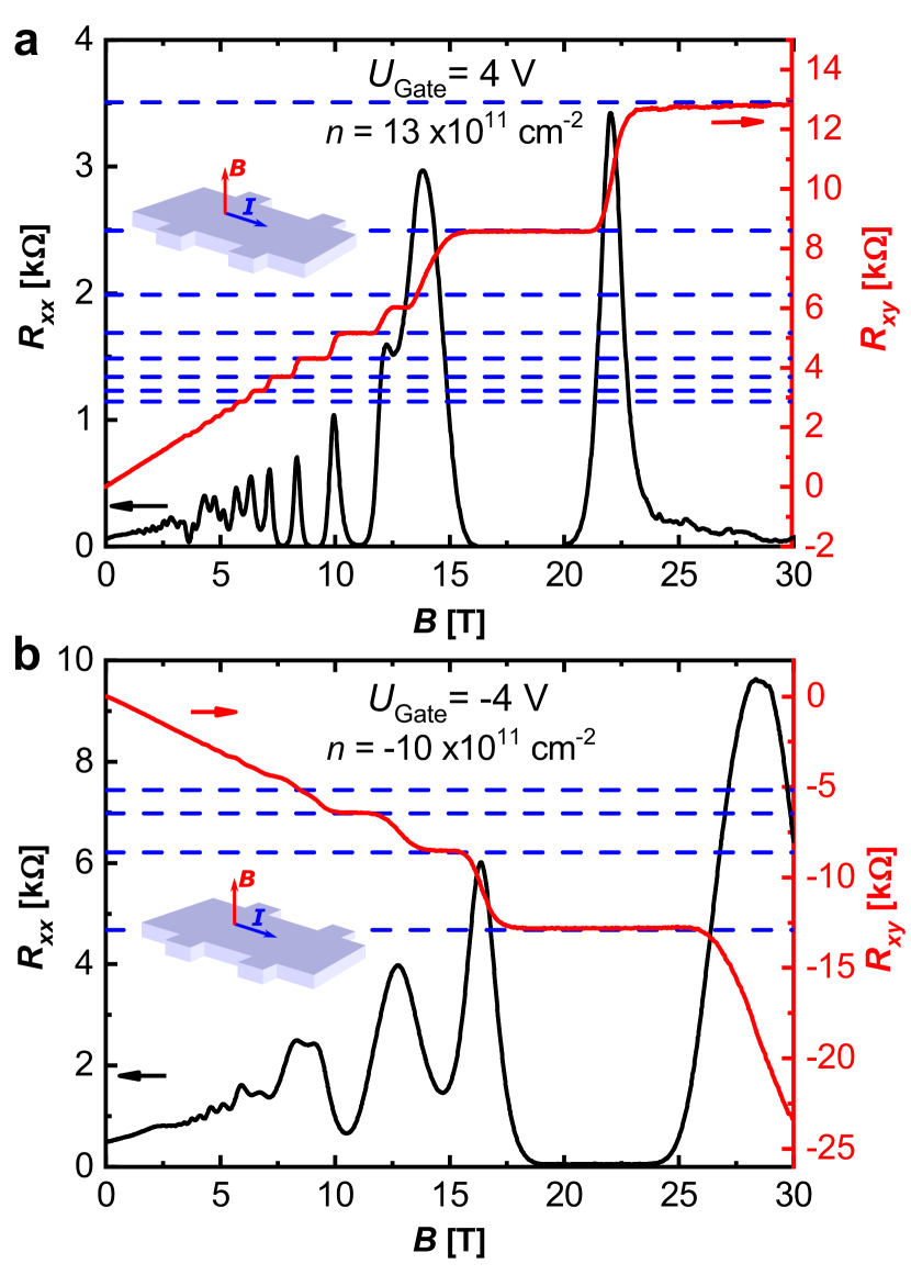
Our devices show sharply distinct transport behavior when the gate is used to introduce additional carriers. This is best observed for measurements in a perpendicular magnetic field. For illustration, Fig. 6 depicts transport data at gate voltages of V corresponding to highly n-type and highly p-type. The curves show Shubnikov-de Haas (SdH) oscillations in together with quantum Hall (QH) plateaus. QH plateaus only exist in two-dimensional systems. Consistently, the maxima of the SdH-oscillations coincide with the transitions between QH plateaus, suggesting that also the longitudinal resistance is driven by the same two-dimensional transport channel. Since the investigated sample is a three-dimensional bulk piece, the two-dimensional character points towards transport carried by a surface state. For this subset of transport contribution, the p-conducting regime (Fig. 6b) differs from the n-conducting regime (Fig. 6a) mainly by overall lower mobility, leading to Landau level broadening, and consequently less pronounced QH plateaus. Mobilities of are observed for electrons and for holes. These numbers are comparable to the ones reported for tensiley strained HgTe Jost et al. (2017), which is a topological insulator Brüne et al. (2014). The accurate quantization of the plateau levels, i.e., exactly equal to the von Klitzing constant to within the experimental accuracy of about , highlights that for these gate voltages, where the surface states are highly populated, the conduction is dominated by surface transport, and bulk Dirac contributions are no longer significant.
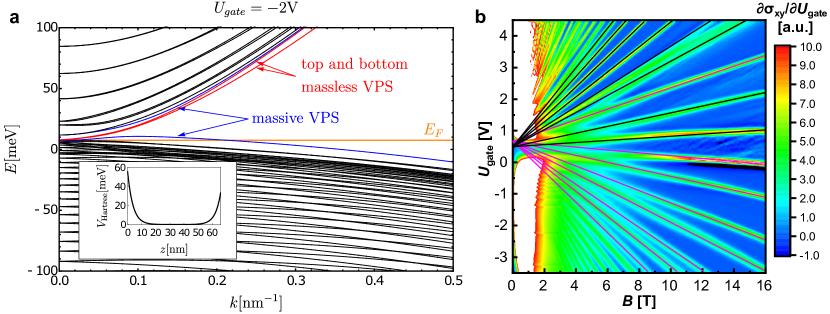
An even clearer picture of the interplay between the bulk and surface sources of conduction contributions emerges from the color scale plot of the gate-voltage derivative of the Hall-conductivity as a function of gate voltage and magnetic field, presented in Fig. 7b. The derivative values of Hall conductivity (designated in color range from green to red) represent the Landau level (LL) dispersion of a two-dimensional system with respect to the magnetic field and the gate voltage . For holes () a regular pattern of Landau levels is observed. The splitting between two subsequent Landau levels iterates with smaller and bigger gap. A zero quantum Hall index is observed for low carrier densities () between two nearly non-dispersive Landau levels, separating the hole and electron regime. The electron transport regime for higher gate voltages () generally shows a regular pattern of Landau levels. The only exception is the ”crossing” of two Landau levels where the quantum Hall index with would be expected. This effect can be ascribed to the overlap of two types of surface state LL fans; the ubiquitous massless Volkov-Pankratov surface states, and the massive Volkov-Pankratov states that arise from the high electric field across the HgTe/(Hg,Cd)Te interfaces Volkov and Pankratov (1985) and which were recently identified in HgTe-based topological insulators Inhofer et al. (2017); Tchoumakov et al. (2017). A qualitative description is motivated by 6 6 kp calculations ( and bands) with hard-wall boundary conditions in the growth direction, including compressive strain and a bulk inversion asymmetry term from DFT calculations, as well as a Hartree potential as in Ref. Brüne et al. (2014). Fig. 7a shows the band structure of a nm thick sample with an applied Hartree potential corresponding to a gate voltage of V (cm-2). Since the gate voltage is applied from the top surface of the system, such a Hartree potential (shown in the inset of Fig. 7a) additionally breaks inversion symmetry. The energies of the massless Volkov-Pankratov states (red) of the top and bottom surface therefore split. Additionally, massive Volkov-Pankratov states (blue) form due to the Hartree potential which confines the bulk states, as also discussed in Ref. Tchoumakov et al. (2017). For negative gate voltage, the hole-like massive Volkov-Pankratov state crosses the Fermi energy (orange) and thus has the most significant contribution to transport properties at this gate voltage. For positive gate voltage, the massless Volkov-Pankratov states dominate the transport behavior since the density of the massive Volkov-Pankratov states is negligible. These calculations allow us to assign the black (magenta) Landau levels in Fig. 7b to massless (massive) Volkov-Pankratov states. To show the evolution of the band structure under gate voltage, we provide additional calculations for V for the nm thick sample in the supplementary material. kp calculations and experimental data for a nm thick sample are presented along with the analogous analysis in the supplementary information See Supplemental Material at xxx. .
From the above detailed analysis, we conclude that our samples display two distinct transport regimes. First, a narrow gate voltage window around the resistance maximum at , where chiral anomaly driven negative magnetoresistance is observed (light blue traces in Fig 4. This effect is only expected from odd-dimensional Dirac cones, in our case the three-dimensional bulk Dirac cones. Second, at higher gate voltages (i.e. for finite/high carrier densities) a two-dimensional transport regime is identified by an emerging quantum Hall effect due to the topological surface state of the band inverted material, slightly modified by topologically trivial (massive) Volkov-Pankratov surface states of the material Volkov and Pankratov (1985). Our observations provide a simple explanation for the recent findings about a quantum Hall effect in Cd2As3 layers Zhang et al. (2017); Schumann et al. (2018) and make it evident that extreme care is needed in claiming any contributions from Fermi arcs in the transport properties of Weyl semimetals in general.
To summarize, compressively strained epitaxial HgTe layers have proven to constitute an ideal platform for controlled and reliable transport experiments on a Weyl/Dirac semimetal. Our experiments emphasize the crucial role played by the inversion-induced massless Volkov-Pankratov surface states in this class of topological materials. As supported by our recent results in this direction, compressively strained HgTe naturally suggest themselves to be an intriguing playground for imposing superconducting proximity effect, where it should be worthwhile probing the superconducting pairing mechanism at Dirac and Weyl nodes.
The work was supported by the DFG (SFB 1170 - ID: 258499086, Leibniz, and ct.qmat EXC2147 – ID: 39085490), the EU (ERC-StG-TOCOTRONICS-Thomale-336012 + ERC-Adv-3TOP-Molenkamp-267436), and the Bavarian ministry of education (ENB and ITI). We acknowledge C. Brüne for useful discussions and F. Schmidt for help with the measurements. The authors gratefully acknowledge the Gauss Centre for Supercomputing e.V. for providing computing time on the GCS Supercomputer SuperMUC at Leibniz Supercomputing Centre (LRZ). Some measurements at high magnetic fields were performed at the HFML, Nijmegen, the Netherlands.
References
- König et al. (2007) M. König, S. Wiedmann, C. Brüne, A. Roth, H. Buhmann, L. W. Molenkamp, X.-L. Qi, and S.-C. Zhang, Science 318, 766 (2007).
- Hsieh et al. (2008) D. Hsieh, D. Qian, L. Wray, Y. Xia, Y. S. Hor, R. J. Cava, and M. Z. Hasan, Nature 452, 970 (2008).
- Brüne et al. (2011) C. Brüne, C. X. Liu, E. G. Novik, E. M. Hankiewicz, H. Buhmann, Y. L. Chen, X. L. Qi, Z. X. Shen, S. C. Zhang, and L. W. Molenkamp, Physical Review Letters 106, 126803 (2011).
- Armitage et al. (2018) N. P. Armitage, E. J. Mele, and A. Vishwanath, Review of Modern Physics 90, 015001 (2018).
- Jay-Guerin et al. (1977) J.-P. Jay-Guerin, M. J. Aubin, and L. G. Caron, Solid State Communications 21, 771 (1977).
- Volkov and Pankratov (1985) B. A. Volkov and O. A. Pankratov, JETP Letters 42, 4 (1985).
- Tchoumakov et al. (2017) S. Tchoumakov, V. Jouffrey, A. Inhofer, E. Bocquillon, B. Plaçais, D. Carpentier, and M. O. Goerbig, Physical Review B 96, 201302(R) (2017).
- Yang and Nagaosa (2014) B.-J. Yang and N. Nagaosa, Nature Communications 5, 4898 (2014).
- Yi et al. (2014) H. Yi, Z. Wang, C. Chen, Y. Shi, Y. Feng, A. Liang, Z. Xie, S. He, J. He, Y. Peng, X. Liu, Y. Liu, L. Zhao, G. Liu, X. Dong, J. Zhang, M. Nakatake, M. Arita, K. Shimada, H. Namatame, M. Taniguchi, Z. Xu, C. Chen, X. Dai, Z. Fang, and X. J. Zhou, Scientific Reports 4, 6106 (2014).
- Arnold et al. (2016) F. Arnold, C. Shekhar, S.-C. Wu, Y. Sun, R. D. d. Reis, N. Kumar, M. Naumann, M. O. Ajeesh, M. Schmidt, A. G. Grushin, J. H. Bardarson, M. Baenitz, D. Sokolov, H. Borrmann, M. Nicklas, C. Felser, E. Hassinger, and B. Yan, Nature Communications 7, 11615 (2016).
- Yoshida (1980) K. Yoshida, Journal of Applied Physics 51, 4226 (1980).
- Reis et al. (2016) R. D. d. Reis, M. O. Ajeesh, N. Kumar, F. Arnold, C. Shekhar, M. Naumann, M. Schmidt, M. Nicklas, and E. Hassinger, New Journal of Physics 18, 085006 (2016).
- Liu and Leung (1975) L. Liu and W. Leung, Physical Review B 12, 2336 (1975).
- Brüne et al. (2014) C. Brüne, C. Thienel, M. Stuiber, J. Böttcher, H. Buhmann, E. G. Novik, C.-X. Liu, E. M. Hankiewicz, and L. W. Molenkamp, Physical Review X 4, 041045 (2014).
- Leubner et al. (2016) P. Leubner, L. Lunczer, C. Brüne, H. Buhmann, and L. W. Molenkamp, Physical Review Letters 117, 086403 (2016).
- (16) See Supplemental Material at xxx., .
- Ruan et al. (2016) J. Ruan, S.-K. Jian, H. Yao, H. Zhang, S.-C. Zhang, and D. Xing, Nature Communications 7, 11136 (2016).
- Wan et al. (2011) X. Wan, A. M. Turner, A. Vishwanath, and S. Y. Savrasov, Physical Review B 83, 205101 (2011).
- Sbierski et al. (2014) B. Sbierski, G. Pohl, E. J. Bergholtz, and P. W. Brouwer, Physical Review Letters 113, 026602 (2014).
- Nielsen and Ninomiya (1983) H. B. Nielsen and M. Ninomiya, Physics Letters B 130, 389 (1983).
- Hosur and Qi (2013) P. Hosur and X. Qi, Comptes Rendus Physique 14, 857 (2013), topological insulators / Isolants topologiques.
- Son and Spivak (2013) D. T. Son and B. Z. Spivak, Physical Review B 88, 104412 (2013).
- Burkov (2015) A. A. Burkov, Physical Review B 91, 245157 (2015).
- Lu and Shen (2015) H.-Z. Lu and S.-Q. Shen, Physical Review B 92, 035203 (2015).
- Zhang et al. (2016) C.-L. Zhang, S.-Y. Xu, I. Belopolski, Z. Yuan, Z. Lin, B. Tong, G. Bian, N. Alidoust, C.-C. Lee, S.-M. Huang, T.-R. Chang, G. Chang, C.-H. Hsu, H.-T. Jeng, M. Neupane, D. S. Sanchez, H. Zheng, J. Wang, H. Lin, C. Zhang, H.-Z. Lu, S.-Q. Shen, T. Neupert, M. Z. Hasan, and S. Jia, Nature Communications 7, 10735 (2016).
- O’Handley (2000) R. C. O’Handley, Modern Magnetic Materials: Principles and Applications (John Wiley & Sons, New York, 2000).
- Jost et al. (2017) A. Jost, M. Bendias, J. Böttcher, E. Hankiewicz, C. Brüne, H. Buhmann, L. W. Molenkamp, J. C. Maan, U. Zeitler, N. Hussey, and S. Wiedmann, Proceedings of the National Academy of Sciences 114, 3381 (2017).
- Inhofer et al. (2017) A. Inhofer, S. Tchoumakov, B. A. Assaf, G. Fève, J. M. Berroir, V. Jouffrey, D. Carpentier, M. O. Goerbig, B. Plaçais, K. Bendias, D. M. Mahler, E. Bocquillon, R. Schlereth, C. Brüne, H. Buhmann, and L. W. Molenkamp, Physical Review B 96, 195104 (2017).
- Zhang et al. (2017) C. Zhang, A. Narayan, S. Lu, J. Zhang, H. Zhang, Z. Ni, X. Yuan, Y. Liu, J.-H. Park, E. Zhang, W. Wang, S. Liu, L. Cheng, L. Pi, Z. Sheng, S. Sanvito, and F. Xiu, Nature Communications 8, 1272 (2017).
- Schumann et al. (2018) T. Schumann, L. Galletti, D. A. Kealhofer, H. Kim, M. Goyal, and S. Stemmer, Physical Review Letters 120, 016801 (2018).