Conductance of gated junctions as a probe of topological interface states
Abstract
Energy dispersion and spin orientation of the protected states at an interface between topological insulators (TIs) and non-topological materials depend on the charge redistribution, strain, and atomic displacement at the interface. Knowledge of these properties is essential for applications of topological compounds, but direct access to them in the interface geometry is difficult. We show that conductance of a gated double junction at the surface of a topological insulator exhibits oscillations and a quasi-linear decay as a function of gate voltage in different regimes. These give the values for the quasiparticle velocities along and normal to the junction in the interface region, and determine the symmetry of the topological interface states. The results are insensitive to the boundary conditions at the junction.
I Introduction
Topological materials Qi and Zhang (2011); Hasan and Kane (2010); Hasan and Moore (2011) acting as components of superconducting or spin-based electronic devices promise metrics exceeding current charge-based technologies Mellnik et al. (2014); Wang et al. (2017a); Rakheja et al. (2019). These functionalities are enabled by the spin-momentum locking of the states localized at the interfaces between topologically trivial and non-trivial compounds. The details of this spin texture as a function of the in-plane momentum control the types of proximity-induced superconducting order Fu and Kane (2008); Alicea (2012), spin accumulation under transport current Burkov and Hawthorn (2010); Pesin and MacDonald (2012), and the gap opening under exchange fields Qi and Zhang (2011); Alicea (2012). Proposed applications of topological insulators (TIs) commonly assume that the interface states have the same linear Dirac-like dispersion and helical spin texture as the states at vacuum TI termination Hasan and Moore (2011). Under this assumption, once material advances eliminated contribution of the bulk states and allowed tuning of the chemical potential Zhang et al. (2011); Arakane et al. (2012), the interface-based devices should have become achievable.
However, topological interface states (TIS) are not guaranteed to be similar to the surface states. Generically, interfaces have lower symmetry than surfaces due to strain, lattice reconstruction, polar charge redistribution, broken bonds, etc. Symmetry breaking (in the absence of fine tuning) simultaneously distorts the Dirac cone and breaks the helicity of the topological states inducing an out-of-plane spin component Zhang et al. (2012); Asmar et al. (2017) thereby dramatically changing the response to the exchange field Asmar et al. (2017) and types of the induced superconducting orders Alspaugh et al. (2018). Therefore, it is highly desirable to have straightforward tests of the symmetry breaking in the TIS.
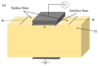
Direct access (ARPES or scanning tunneling spectroscopy) to the TIS is very challenging due to the capping material, and indirect optical measurements (e.g. Kerr rotation Wang et al. (2017b); Mondal et al. (2018)) are often hard to interpret. Here we demonstrate that the dc conductance in a gated double junction setup for a topological heterostructure, shown in Fig. 1(a), exhibits a quasi-linear variation in one range, and Fabry-Perot-like oscillations in another range of gate voltages. The ”kink” voltage at the edge of the linear regime and the period of the oscillations give the quasiparticle velocities parallel and normal to the junction, and hence the dispersion anisotropy of the hidden topological interface state. Symmetry considerations supported by model calculations Zhang et al. (2012); Asmar et al. (2017) dictate that this anisotropy is accompanied by the tilting of the spins out of the plane of the interface.
The experiment we propose does not quantify the degree to which spin is tilted away from the plane of the interface, and only detects if this tilting is present. However, its advantage is that it uses straightforward conductance measurements, and is robust with respect to the scattering at the junction, see below. Therefore we believe that the proposed method can be easily used to check whether the spins are helical and whether the junction should exhibit behavior suggested by simplified models. In addition, our analysis of the role of junction scattering offers a clear perspective on the role of this, inevitably present, phenomenon, on the topological properties of prototype devices.
Previous studies considered Fabry-Perot-induced transmission resonances in gated graphene junctions Beenakker (2008); Castro Neto et al. (2009), but, in contrast to that case, the physics discussed here relies on the spinor structure of the TIS. Conductance oscillations were predicted in the TI surface states subject to the exchange field in the gated region Mondal et al. (2010); Soori et al. (2012), but those studies assume no distinction between the interface and the surface states, and ignore the scattering at lateral junctions, which we show to be a critical consideration. Our proposal provides a quantitative measure of symmetry-breaking effects intrinsic to the interface. We also show that the results are robust with respect to the details of the junction scattering not .
The rest of the paper is organized as follows. In Sec. II we explain our model, and the methods we use to obtain the conductance. Sec. III gives the simplest possible example of a non-trivial junction, that with two distinct helical Dirac cones, and elucidates the essential physics at play. The symmetry-broken case is considered in Sec. IV, where we focus on the information on the anisotropy of the Dirac cone that can be extracted from the conductance measurements, and its connection to the spin texture of the interface states. Sec. V summarizes our findings, provides the context for their interpretation, and discusses possible further advances.
II Lateral Junctions
Bulk-boundary correspondence guarantees the existence of a localized state at the interface between a TI and a non-topological material Qi and Zhang (2011); Hasan and Kane (2010). In the absence of time-reversal breaking perturbations, this state is generically gapless and, at low energy, linearly dispersing with the momentum in the plane of the interface, . Since the band inversion, which is responsible for the topological properties of the TI, arises from the spin-orbit interaction (SOI), the resulting states also characteristically exhibit spin-momentum locking Qi and Zhang (2011); Hasan and Kane (2010); Hasan and Moore (2011).
For prototypical TI Bi2Se3, the states at the surface terminations along the high symmetry directions ([111] in the rhombohedral/[001] in the hexagonal representation) are described by the effective Dirac Hamiltonian (Zhang et al., 2009)
| (1) |
where is the vector of the Pauli matrices, is the normal to the surface, is the effective velocity, is the momentum in the - plane, and we set . The eigenstates of Eq. (1) have isotropic dispersion, , and are helical (spin in the interface plane normal to the momentum direction), with the spinor structure
| (2) |
where the angle between and the -axis.
Once the rotation symmetry is broken either by a choice of the lattice termination Zhang et al. (2012) or by the interface potentials Asmar et al. (2017), the topological state is described by a generalized form of , namely
| (3) |
where the sum is over all the spin components, , but the momentum is in the plane, , and the coefficients are real. The eigenstates of have anisotropic dispersion,
| (4) |
with non-helical spin texture and spins that point out of the plane if . It is important to note that this Hamiltonian arises from the microscopic analysis, so that the terms leading to the anisotropy are linear in , and the coefficients are uniquely determined by the bulk properties and interface potentials Asmar et al. (2017). These potentials depend on the details of the constituent materials and growth process, and hence a priori are unknown. Therefore, for a generic interfacial topological state, the anisotropic dispersion persists at low energies, in contrast to the anisotropies induced in the surface states by the higher order, in , terms proposed Fu (2009), for example, for Bi2Se3 and Bi2Te3 due to hexagonal warping of the crystal. It is also important to note that the dependence of on the interface potentials is such that the Hamiltonian, Eq. (3), reduced to Dirac hamiltonian, Eq. (1), for the surface states, i.e. when any of these potentials allowed by symmetry become large Asmar et al. (2017).
Given that there are six independent coefficients in Eq. (3), complete characterization of a specific interface requires performing several indirect measurements, and modeling the results. A simpler, and more practical, question, is what symmetries are broken at a specific interface, and what the consequences of this symmetry breaking for the dispersion and spin-momentum locking of the topological state are. This is the task that, as we show, can be accomplished via conductance measurements on lateral junctions, and below we provide a detailed analysis of such a setup.
The choice of a lateral junction, surface state in prototypical TIs are well established, and therefore the parameter in the surface Dirac Hamiltonian, Eq. (1), is known. As we see below, it is gating of the interface region that enables the information on the symmetry breaking in the hidden TIS to be extracted from conductance measurements. In the following we assume that the bottom surface of the TI is far enough to not hybridize with the top surface, and therefore focus our attention on the top surface near the contacts.
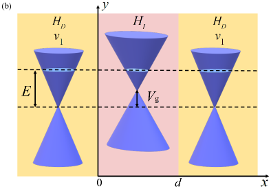
The two types of Dirac dispersion, for the surface and the interface states respectively, are shown in Fig. 1(b). We model this junction by a piecewise Hamiltonian,
| (5) |
The propagating eigenstates in each region are
| (6) | |||||
| (7) |
Here is the spinor of the helical Dirac state, Eq. (2), and is the corresponding spinor for , which depends on the choice of the coefficients , and will be given below for the specific cases we consider. The solutions of the eigenvalue equation are constructed by matching these solutions at the boundaries.
The energy and the momentum along the junction (-axis in Fig. 1(b)) is conserved, . Since the Hamiltonian is linear in , and the momentum along the junction (-axis in Fig. 1(b)) is conserved, the eigenvalue differential equation along the normal ( direction) is of first order. Hence the wave functions need not be continuous McCann and Fal’ko (2004); Basko (2009); Akhmerov and Beenakker (2008), but, instead, at have to satisfy
| (8) |
where denotes the side of the junction. Since spin is conserved in scattering on non-magnetic potentials, the form of the matrix , which connects the spinors on both sides of the junction, relates the spin content of the transmitted, incoming, and reflected states. The matrix has to preserve the time-reversal invariance of the Hamiltonian, i.e. , where denotes complex conjugation. It also has to conserve the particle current normal to the junction.
The particle current operator in each region is given . Therefore, for a piecewise defined Hamiltonian, the current operator is also defined in each region, and the current conservation at each junction demands that
| (9) |
It follows that the boundary matrix must satisfy
| (10) |
For linear in hamiltonians is momentum-independent. Under these conditions Eq. (10) defines a single parameter family of matrices Sen and Deb (2012); Isaev et al. (2015); Tanhayi Ahari et al. (2016), . The physical origin of this degree of freedom is that in the microscopic formulation time-reversal invariance allows spin-independent potential barrier at the junction. The height of this barrier (apriori unknown and difficult to control in experiment) is encoded in the parameter . The exact relationship between the two can be derived E.Thareja and Vekhter , but is not important for the discussion below. Assuming that we cannot experimentally control the value of at each junction implies that we need to show that our predictions are insensitive to it.
Below, for several choices of the symmetry of , we determine the matrix , and use it to compute transmission () and scattering () matrices, see Appendix. This yields the transmission coefficient, as a function of the energy, , and the incident angle, , for different gate voltages, , and the boundary coefficients at each junction. For a single junction the transmission is dominated by Klein tunneling at normal incidence, , irrespective of the choice of , . The anisotropy of the Dirac states, and details of the junction potentials appear as very weak features for nearly grazing angles, and therefore are not clearly manifested in the conductance. These features, however, are brought to the fore by the Fabri-Perot oscillations in the double junction setup of Fig. 1(a). We use the transmission coefficients for the double junction to evaluate the low temperature conductance using Landauer formalism,
| (11) |
where , the width of the junction, is the chemical potential, and the Fermi momentum is determined from the dispersion of the surface states, .
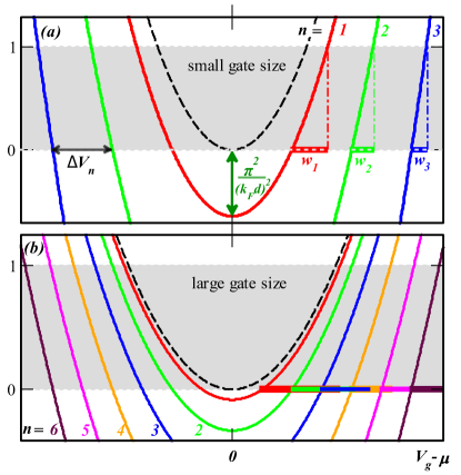
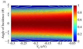
Gating the interface state by the gate voltage changes the size of the Fermi surface in the interface region, see Fig. 1(b). Together with the momentum conservation along the junction, this enables directional-dependent probing of the Dirac cone. The key to understanding the physics behind this directional dependence is to recognize that there are two distinct regimes of the behavior of the conductance as a function of . These regimes are easily understood from the analysis of the simplest cases, presented in next section.
It is appropriate to comment on the potential experimentally relevant aspects of the physics that are left out of this model. First, we consider only the surface and interface states, and neglect the contribution of the bulk bands. Since in experiment the chemical potential can be tuned by alloying Zhang et al. (2011); Arakane et al. (2012), we believe that this regime is experimentally achievable. In more general terms the applications of the TIs mostly rely on eliminating, or substantially reducing, the bulk contributions, and therefore we follow a well-trodden path in making this assumption. Second, in some TIs a 2DEG forms after some time in the vacuum chamber Bianchi et al. (2010). Potentially this can be avoided by capping the TI with a very large gap semiconductor, when the distortion of the surface states is minimal Asmar et al. (2017). Moreover, this 2DEG is formed at energies of the order of the bulk gap, and therefore tuning the chemical potential close to the Dirac point and using small gate voltages ensures that it does not poison the conductance measurements. The same small values of the gate voltage relative to the bulk gap value ensure that we do not need to consider hexagonal distortion that is cubic in the distance to the Dirac point in the momentum space, and therefore is not relevant at low energies. In all of the following we restrict ourselves to parameters satisfying these constraints.
III Helical Interface State
III.1 Conductance of gated junctions and the Dirac velocity.
Most of the relevant physics can be inferred from considering the simplest possible case, where the interface state is also helical, , as illustrated in Fig. 2. One of the simplifications is that the matrix form of the particle current operator in the direction normal to the junction is the same in all regions defined by the Hamiltonian, Eq. (5), namely . Substituting in Eq. (10) yields
| (12) | |||||
| (13) |
for the junctions at and respectively, with arbitrary real parameters. The form of the boundary matrix is easy to understand if we realize that the rotations in the spin space around the -axis leave the current operator invariant. The ratio of the velocities ensures conservation of the probability current.
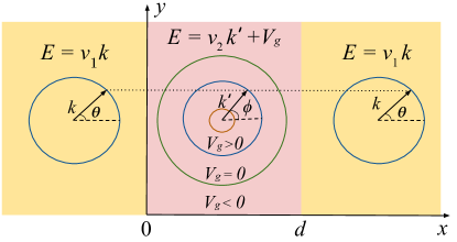
The role of gating is qualitatively clear from Fig. 2, where we graphically show the consequences of the conservation of the energy, (note that we plot only , since, in the low energy theory, the physical picture is symmetric with respect to , and we discuss corrections to this picture separately below), and the momentum along the junction,
| (14) |
where and are the directions of propagation of the quasiparticles in the surface and interface regions respectively. At low temperatures, , we can set for the quasiparticles contributing to the conductance without loss of generality. For sizeable positive bias, , only the particles at near-normal incidence from the region may enter the interface region. The transmission for near-normal incidence is close to unity, but the density of states in the interface region is low due to small size of the Fermi surface, and is the main limiting factor for transport. Consequently, we expect the conductance to be essentially linear in the gate voltage, , in the vicinity of (quasiparticle energy in the interface region tuned to the Dirac point), with additional, weaker, variations due to the matching conditions at the second junction, .
For sufficiently negative bias, , the momentum conservation dictates that all the incident quasiparticles from the surface states travel nearly along the -axis in the interface region. Consequently we expect Fabri-Perot oscillations with the phase acquired in this region, with maxima at
| (15) |
corresponding to the periodicity with the gate voltage,
| (16) |
Note that, because of Klein tunneling, the quasiparticles at exactly normal incidence do not contribute to the oscillations. Therefore, the overall transmission is high (conductance ), and we expect the amplitude of the oscillations to be a fraction of the total conductance, in contrast to the usual Fabri-Perot interferometer. We see below that this fraction, however, is substantial under realistic assumptions.
The crossover between the two regimes occurs when the two Fermi surfaces are of the same size, at the gate voltages
| (17) |
which we label “kink” voltages hereafter. For the density of states effects dominate, and the conductance is suppressed. Outside of this range the double junction is highly transparent, and the oscillations due to the phase acquired in the interface region are clearly observable.
Detailed calculations confirm these expectations, and allow the analysis of their dependence on the boundary angles and . Appendix A gives the details of the derivation of the transmission coefficient by matching the wave functions at both linear junctions, and yields
| (18) |
where we denoted the phase accumulated while traversing the interface region , and introduced , and . This expression, together with Eq. (11), is used to evaluate the conductance for specific parameter values.
We set the Dirac velocity of the surface state to its experimental value Kuroda et al. (2010); Chang et al. (2015) for Bi2Se3, Kuroda et al. (2010); Chang et al. (2015) . We use eV in most of our calculations, so that we stay close to the Dirac point, and can ignore the hexagonal warping, bulk band transport, and possible formation of the 2DEG at the interface. This choice gives Å-1. Realistic device sizes then imply . In most of our calculations we set nm (), which allows coherent quasiparticle propagation across the gated region according to the values of the mean free path reported for and Bi2Se3 Dufouleur et al. (2017); Kamboj et al. (2017); Chen et al. (2013)( nm), and especially for close to the Dirac point Kellner et al. (2015), but also consider other values of for the situation where this is relevant, see below.
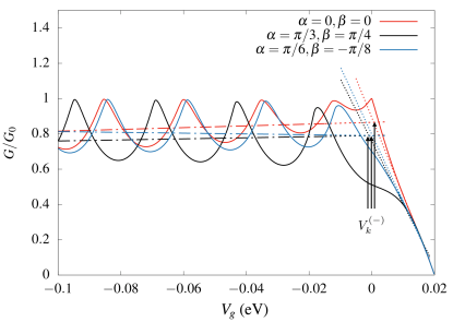
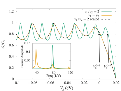
It is important to understand that the oscillations are present even if the Dirac velocities in the two regions are identical, , as shown in Fig. 3. The gated region creates mismatch of the Fermi surfaces, and the conductance shows the two regimes discussed above, namely the linear decrease near , and the oscillatory high conductance region away from that value. Importantly, Fig. 3 shows that the kink voltage, in this case (cf. Eq. (17)), is insensitive to the junction scattering parameters . For practical purposes, we define this voltage as the intersect between linear fit to in two regimes. First, at greater , we average the conductance over one oscillation period, and perform a linear fit for the resulting values. Second, we extend the linear near . These lines are shown in Fig. 3, and their intercept defines . Even though the slope near varies by about 20% as vary, the intercept only changes by about 5% across those values. We find the same behavior for ; Moreover, we find that the difference between the kink voltages determined from the intercept for different , and the value given by Eq. (17) decreases with the increased mismatch of the Dirac velocities.
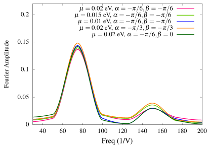
It is also clear from Fig. 3 that junction scattering changes the phase of the oscillations at , but leaves the period unchanged, and we now show this in more detail by comparing the results for and in Fig. 4 for a select (non-trivial choice of junction scattering. Arrows indicate the kink voltages determined from the intercept as described above, and correspond very well to the values of and eV respectively. Moreover, the plots for the two cases coincide exactly after rescaling the gate voltage by the ratio , verifying that the Dirac velocity is the sole control parameter for both the kink voltage and the oscillation frequency in the double junction. Inset shows the Fourier transform of the oscillatory part of the conductance, and the main peaks of the Fourier amplitude correspond very well to the frequencies eV-1 and eV-1 for and respectively, obtained from Eq. (16). We also verified that these frequencies are insensitive to the choice of the scattering parameters, or, equally important, to the exact choice of the chemical potential, , as shown in Fig. 5.
Therefore the profile of the conductance in a gated double junction yields, for fully symmetric surface and interface states, two distinct methods for evaluating the Dirac velocity in the interface region: from the kink voltage, , and from the oscillation period, . In the following section we show that, for anisotropic, symmetry-broken, interface states, the two methods give the values for the Dirac velocity in the two orthogonal directions, parallel and normal to the junction, and therefore can be used to quantitatively determine the anisotropy of the Dirac dispersion. Before we do that it is helpful to understand better the origin of the oscillations.
III.2 Transmission probability and conductance oscillations.
We focus first on the negative gate voltages: while the simple low energy theory is symmetric with respect to the Dirac point, in many topological insulators of the Bi2X3 family the Dirac point is close to the top of the valence band, making this a natural choice. From Eq. (14) the direction along which a quasiparticle travels in the interface region is
| (19) |
Therefore for sufficiently large bias, compared to the kink voltage, when , we have , and quasiparticles in the gated region move nearly normal to the interface, see Fig. 2. If we set in the expression for the transmission coefficient, Eq. (18), we obtain
| (20) |
where , and . This yields an approximate analytical expression for the conductance
| (21) |
with
| (22) |
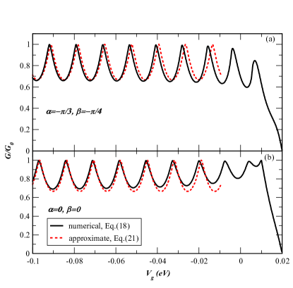
Fig. 6 shows that this expressions provides an excellent agreement with our results. Eq. (21) also explains why inclusion of the boundary scattering gives simply a phase shift at large gate voltages, and gives a seemingly universal amplitude of the oscillations, since the maxima and minima of the function are and respectively.
The evolution of the oscillations with the width of the gated region is more complicated, however. For large assuming normal travel in the gated region is justified everywhere in Eq. (18) except in the Fabri-Perot phase, , where the small variations in the angle are multiplied by a potentially large factor , leading to substantial variations in the contributions to the conductance. Requiring yields a much more restrictive condition on the applicability of Eq. (21), namely
| (23) |
In the opposite regime of large , the Fabri-Perot phase oscillates rapidly relative to the variation of the incidence angle, , where . Therefore we can obtain the approximate expression for the conductance by first averaging over a period of the Fabri-Perot oscillations in Eq. (21), i.e.
This value of the conductance, is in a very good agreement with the numerical results presented in Fig. 7. As expected, the oscillation amplitude is significantly reduced in this regime.
Qualitatively, if , the rapid oscillations of the Fabri-Perot phase with the incidence angle, , in Eq. (20), lead to rapid variations of the transmission probability with , with dominant contributions coming from the “angles of perfect transmission”, , which occur: (a) for normal incidence, (Klein tunneling); (b) when , corresponding to the incidence angles
| (25) |
The number of such angles for a gives voltage is determined by
| (26) |
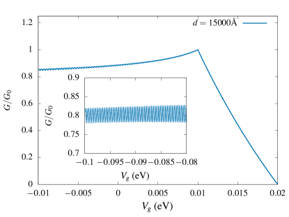
It is obvious that the allowed values of here strongly depend on the magnitude of . Fig. 8 shows a graphical solution of Eq. (25) for the cases of small () and large () gated region length. In the former case, Fig. 8(a), the perfect transmission maxima only occur in narrow ranges of the gate voltages, which become more and more widely separated as increases. For a long gate there are sometimes several such maxima at gate voltages close to the chemical potential, see Fig. 8(b). In principle, as increases, at large we cross over to the well-separated maxima regime akin to that of Fig. 8(a) since the displacement of parabolas varies as , but whether this regime is reached for experimentally relevant parameter values depends on the specifics of the material.
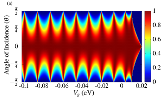
The general behavior of the transmission coefficients for different choices of are shown in Fig. 9. Note that for smaller gated length is generally featureless, with maximum at normal incidence. As the gate voltage is swept from minimum to the maximum of the conductance, the transmission coefficient at every angle changes accordingly, see Fig. 9(a), in agreement with Eq. (20). For larger , Fig. 9(b), transmission maxima appear at angles . These angles are shifted as the gate voltage varies, leading to small amplitude of conductance oscillations in this regime.
The entire behavior of the conductance as a function of both voltage and the incidence angle is summarized in Fig. 10. At small to moderate values of , Fig. 10(a), the periodic pattern or large vs small transmission at finite incidence angles is very clear, with deep troves in between. As this parameter becomes greater, however, see Fig. 10(b) where we considered a greater values of and to bring out the features more clearly, multiple transmission peaks are present, the number of such peaks depends on the gate voltage, and the oscillation amplitude, which is the weighted integral of , is reduced.
In summary, here we showed that, given knowledge of the surface state dispersion in a topological insulator, , we can determine the Dirac velocity of the quasiparticles in the (inaccessible to surface probes) interface region from the behavior of the conductance of a double junction using either the kink voltage, Eq. (17), or period of the oscillations, Eq. (16). For the current generation of topological insulators such as Bi2Se3, to stay well below the bulk gap we estimate the maximal value of the gate voltage, eV (taking half of the gap value as the rough guide), implying that the chemical potential should stay below about half of that value to ensure sufficient range of oscillations, eV, translating into Å. Therefore, the values of roughly Å correspond to small gate, while Å correspond to large gate regimes. The nature and origin of the oscillations are slightly distinct between the two regimes, and we provided both analytical and numerical evaluations of both.
Crucially, our results are insensitive to the boundary scattering at lateral junctions, and therefore applicable for a wide range of techniques of sample preparation. We now show that this seeming redundancy in determining can be used to quantitatively determine the anisotropy of the interface Dirac states when the symmetry is broken in the interface region.
IV Non-helical interface states
The above analysis was for a system with the simplest possible effect of the interface: velocity renormalization of the helical states. The key question is whether the interface states with broken rotational symmetry (and therefore non-helical) can be detected and characterized by the proposed method. The answer is affirmative, and we give the details here. Ref. Asmar et al., 2017 gave the symmetry analysis of all possible interface state Hamiltonians linear in , see Eq. (3), and we focus on the most interesting case considered there. When the spin-rotation invariance is broken, the residual symmetry of is reduced to the representation of the symmetry group, the Dirac dispersion becomes anisotropic, with elliptical constant energy contours, and the spins of the interface states point out of the plane of the interface. To capture these effects, we consider
| (27) |
equivalent to that analyzed in Ref. Asmar et al., 2017. In simple models the values of depend on the interface potentials, and generically, without fine tuning, whenever . For we recover the helical interface state case discussed in the previous section). The energy dispersion of ,
| (28) |
is anisotropic, with elliptical constant energy contours.
It is convenient to introduce the following notations,
| (29a) | |||
| (29b) | |||
| (29c) | |||
Then the eigenvector of the interface hamiltonian, , corresponding to the eigenvalue, , is given by
The eigenstate is non-helical, and the spins tilt out of the plane of the interface, with the maximal out-of-plane polarization is at . In Eq. (27) we made the natural assumption that symmetry breaking (e.g. due to strain) yields the principal axes for the ellipse which are parallel and perpendicular to the interface. The spins acquire a non-zero out-of-plane component for .
As discussed in the previous sections, for each choice of the interface Hamiltonian, we need to derive the appropriate boundary conditions, conserving the particle current normal to the interface. Here at the left interface in Fig. 1, we have , while , so that the matrix satisfying Eq. (10) has the form
Here is the parameter encoding the potential scattering at the junction. Similarly, for the right junction . We then compute the transmission coefficient and the conductance as described above.
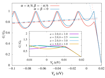
The main features of the conductance as a function of , shown in Fig. 11, are similar to those for the simple interface considered in previous section. When the Dirac point is close to the chemical potential is quasi-linear due to the reduction in the density of states. For large mismatch of the Fermi surfaces between the surface and the interface regions, we observe the conductance oscillations. However, the two regimes are now controlled by the Fermi velocities in different directions.
Recall that the kink voltage, , corresponds to the maximal magnitude of for which the conservation of the momentum along the junction still allows transmission for any incidence angle, see Eq. (14). As the quasiparticle velocity along the junction in the interface region is , see Eq. (28), the kink voltage depends only on that value, and is still given by Eq. (17). Fig. 11 indeed shows that the kink voltage obtained from the full numerical evaluation is in agreement with that value, and only weakly depends on the junction scattering parameters, . In contrast, the initial slope, , is more sensitive to these parameters. Fig. 11(b) also confirms that the kink voltage is completely insensitive to the choice of the anisotropy parameters and .
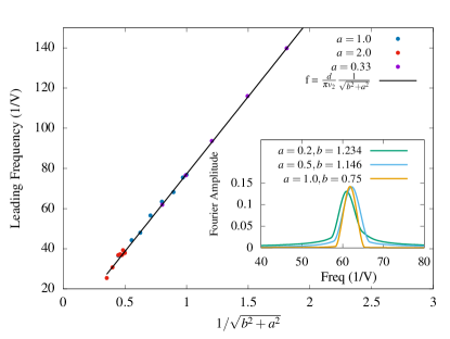
In the oscillatory regime, as discussed in the previous section, a good approximation for the conductance oscillations is obtained by assuming that in the interface region the quasiparticles propagate nearly normal to the junction. Therefore the relevant velocity is , and we expect the leading oscillation frequency to be given by the corresponding modification of Eq. (16), namely,
| (32) |
Indeed, the lead frequency of the Fourier transform of the conductance oscillations, plotted in Fig. 12 shows an excellent agreement with this expression. It is also essentially independent of the junction scattering.
Consequently, in the more general case considered here, measurements of the kink voltage and the lead frequency of the conductance oscillations give the values for the quasiparticle velocities in the interface region along and normal to the interface respectively, this giving a quantitative measure of the anisotropy (or lack thereof) of the topological states in the otherwise inaccessible interface region. To our knowledge this is the first proposal for such a measurement.
V Discussion and conclusions
In summary, we addressed here a problem of general interest for prototypical topological devices. The functionality of such devices relies on interface, rather than the surface, topological states, but the interface potentials may break the full rotational symmetry of the low-energy topological states already at the level of linear, in the momentum, terms in the effective Hamiltonian. Given that the interface states are not easily accessible by spectroscopic probes such as STM or ARPES, the question of how to detect this broken symmetry is relevant and timely. Symmetry breaking of the interface states has implications for a wide variety of devices of interest that depend on using topological states from TI based ferromagnetic devices to TI based Josephson junctions which have been shown to host the famous zero-energy Majorana fermions.
We showed that the conductance of a gated mesoscale double junction at a surface of topological insulator can be used to quantitatively determine the anisotropy (or lack thereof) of the quasiparticle dispersion normal to and along the junction in the (otherwise hidden) interface region. We demonstrated that the features we use to extract these parameters, the kink and the period of Fabri-Perot-like oscillations of conductance as a function of gate voltage, are robust against scattering at the junctions, and independent of the exact location of the chemical potential, provided the bulk band contribution to the conductance and other experimentally controlled extrinsic effects remain small.
While the broken rotational symmetry of the interface states indicates that these states are non-helical, and, generally, in the absence of fine-tuning, requires out of plane spin-tilt of the topological states, the measurement we propose does not directly detect this out of plan spin component. A different set of measurements, possibly under applied magnetic field, is required to do this, and will be addressed separately. However, observation of the anisotropy in the quasiparticle dispersion for the topological states would in itself be an important step towards understanding, further analyzing from the first-principles perspective, and ultimately controlling, the topological interface properties for prototype devices.
Acknowledgements.
We thank D. Alspaugh and D. E. Sheehy for discussions. This research was supported in part by NSF via Grant No. DMR-1410741 (E. T., I. V., M. M. A.) and No. DMR-1151717 (M. M. A.).Appendix A Helical Interface State
In this appendix, we detail the and -matrix based method used to calculate transmission probability.
To begin we recall that the Hamiltonian of the gated double junction is given by
| (33) |
We can write the eigenvectors for positive energy , in different regions as
| (34) |
| (35) |
| (36) |
In the latter equations we used due to translational invariance along the -direction and defined sgn . Before preceding to solve the boundary conditions at and junction it is convenient to define the matrix,
| (37) |
We notice that for different parameters , and in the matrix make its columns the eigenvector components in the different scattering regions. Returning to the boundary condition at the first junction, , we notice that
| (38) |
Similarly, at the second junction (),
| (39) |
Using the above two boundary conditions one can write
| (40) |
and from the equation above we can identify the transmission-matrix (-matrix), where
| (41) | |||||
Here we note that the presence of the junction-potentials modify the -matrix, from its conventional form with , where is the identity matrix), via the matrices and which encapsulate the scattering sources via and at their respective junctions. The -matrix is related to the scattering-matrix (-matrix) by
| (42) |
The elements of the -matrix allow us to determine the transmission and reflection coefficients of the multi-junction scattering problem, such that and . Finally, the transmission probability is given by .
Appendix B Non-Helical Interface State
In this section we detail the method used to calculate the transmission probability for the junctions with non-helical state. The Hamiltonian for our setup is given by
| (43) |
In the main text, eigenenergy of region II was written as and the energy eigenfunction as
| (44) |
where and , are defined in Eq. (29). While this notation is analytically convenient, we switched to a different notation while calculating transmission probability for numerical efficiency. We outline the steps below. Consider the expressions below rewritten using Eq. (29)
| (45) |
| (46) |
| (47) |
| (48) |
With these definitions we can write the non helical Hamiltonian as:
| (49) |
The latter Hamiltonian is characterized by the eigenvalues . Considering the positive eigenenergies, its associated eigenspinor for is given by
| (50) |
where
| (51) |
In the regions I and III the eigenstates are given in Eqs. 34 and 36, respectively, while in the region II the eigenstates are
where we have defined
| (53) |
is given in Eq. (51), corresponds to the angle between momentum and the -axis. The eigenvector with coefficient is travelling towards right while the one with coefficient is travelling towards left after reflecting from region III.
In this case it is we need to define an independent matrix for the non helical region with columns consisting of the eigenstates in this region, where
| (54) |
where are given in Eq. (53). With this definition the boundary condition at the first junction at becomes
| (55) |
where matrix is defined in Eq. (37). Similarly, at the second junction ,
| (56) |
Finally, we can relate the coefficients at the two ends the system, such that
| (57) | |||||
and this implies that the -matrix is
From the -matrix one can obtain the -matrix as previously shown. Then the transmission probability is given by . By integrating the transmission probability, one can obtain the conductance of the device, which as shown in the main text.
References
- Qi and Zhang (2011) X.-L. Qi and S.-C. Zhang, Rev. Mod. Phys. 83, 1057 (2011).
- Hasan and Kane (2010) M. Z. Hasan and C. L. Kane, Rev. Mod. Phys. 82, 3045 (2010).
- Hasan and Moore (2011) M. Z. Hasan and J. E. Moore, Annual Review of Condensed Matter Physics 2, 55 (2011) .
- Mellnik et al. (2014) A. R. Mellnik, J. S. Lee, A. Richardella, J. L. Grab, P. J. Mintun, M. H. Fischer, A. Vaezi, A. Manchon, E.-A. Kim, N. Samarth, and D. C. Ralph, Nature 511, 449 EP (2014).
- Wang et al. (2017a) Y. Wang, D. Zhu, Y. Wu, Y. Yang, J. Yu, R. Ramaswamy, R. Mishra, S. Shi, M. Elyasi, K.-L. Teo, Y. Wu, and H. Yang, Nature Communications 8, 1364 (2017a).
- Rakheja et al. (2019) S. Rakheja, M. E. Flatté, and A. D. Kent, Phys. Rev. Applied 11, 054009 (2019).
- Fu and Kane (2008) L. Fu and C. L. Kane, Phys. Rev. Lett. 100, 096407 (2008).
- Alicea (2012) J. Alicea, Reports on Progress in Physics 75, 076501 (2012).
- Burkov and Hawthorn (2010) A. A. Burkov and D. G. Hawthorn, Phys. Rev. Lett. 105, 066802 (2010).
- Pesin and MacDonald (2012) D. Pesin and A. H. MacDonald, Nature Materials 11, 409 EP (2012).
- Zhang et al. (2011) J. Zhang, C.-Z. Chang, Z. Zhang, J. Wen, X. Feng, K. Li, M. Liu, K. He, L. Wang, X. Chen, Q.-K. Xue, X. Ma, and Y. Wang, Nature Communications 2, 574 (2011).
- Arakane et al. (2012) T. Arakane, T. Sato, S. Souma, K. Kosaka, K. Nakayama, M. Komatsu, T. Takahashi, Z. Ren, K. Segawa, and Y. Ando, Nature Communications 3, 636 (2012).
- Zhang et al. (2012) F. Zhang, C. L. Kane, and E. J. Mele, Phys. Rev. B 86, 081303(R) (2012).
- Asmar et al. (2017) M. M. Asmar, D. E. Sheehy, and I. Vekhter, Phys. Rev. B 95, 241115(R) (2017).
- Alspaugh et al. (2018) D. J. Alspaugh, M. M. Asmar, D. E. Sheehy, and I. Vekhter, Phys. Rev. B 98, 104516 (2018).
- Wang et al. (2017b) Y. Wang, D. Zhu, Y. Wu, Y. Yang, J. Yu, R. Ramaswamy, R. Mishra, S. Shi, M. Elyasi, K.-L. Teo, Y. Wu, and H. Yang, Nature Communications 8, 1364 (2017b).
- Mondal et al. (2018) R. Mondal, Y. Saito, Y. Aihara, P. Fons, A. V. Kolobov, J. Tominaga, S. Murakami, and M. Hase, Scientific Reports 8, 3908 (2018).
- Beenakker (2008) C. W. J. Beenakker, Rev. Mod. Phys. 80, 1337 (2008).
- Castro Neto et al. (2009) A. H. Castro Neto, F. Guinea, N. M. R. Peres, K. S. Novoselov, and A. K. Geim, Rev. Mod. Phys. 81, 109 (2009).
- Mondal et al. (2010) S. Mondal, D. Sen, K. Sengupta, and R. Shankar, Phys. Rev. Lett. 104, 046403 (2010).
- Soori et al. (2012) A. Soori, S. Das, and S. Rao, Phys. Rev. B 86, 125312 (2012).
- (22) The effect of the in-plane field in our model is much more complex, anisotropically gapping the tis spectrum and modifying the boundary conditions, and hence deserves a separate study .
- Zhang et al. (2009) H. Zhang, C.-X. Liu, X.-L. Qi, X. Dai, Z. Fang, and S.-C. Zhang, Nature Physics 5, 438 EP (2009), article.
- McCann and Fal’ko (2004) E. McCann and V. I. Fal’ko, Journal of Physics: Condensed Matter 16, 2371 (2004).
- Basko (2009) D. M. Basko, Phys. Rev. B 79, 205428 (2009).
- Akhmerov and Beenakker (2008) A. R. Akhmerov and C. W. J. Beenakker, Phys. Rev. B 77, 085423 (2008).
- Sen and Deb (2012) D. Sen and O. Deb, Phys. Rev. B 85, 245402 (2012).
- Isaev et al. (2015) L. Isaev, G. Ortiz, and I. Vekhter, Phys. Rev. B 92, 205423 (2015).
- Tanhayi Ahari et al. (2016) M. Tanhayi Ahari, G. Ortiz, and B. Seradjeh, American Journal of Physics 84, 858 (2016) .
- Kuroda et al. (2010) K. Kuroda, M. Arita, K. Miyamoto, M. Ye, J. Jiang, A. Kimura, E. E. Krasovskii, E. V. Chulkov, H. Iwasawa, T. Okuda, K. Shimada, Y. Ueda, H. Namatame, and M. Taniguchi, Phys. Rev. Lett. 105, 076802 (2010).
- Chang et al. (2015) C.-Z. Chang, P. Tang, X. Feng, K. Li, X.-C. Ma, W. Duan, K. He, and Q.-K. Xue, Phys. Rev. Lett. 115, 136801 (2015).
- (32) E.Thareja and I. Vekhter, Unpublished.
- Dufouleur et al. (2017) J. Dufouleur, L. Veyrat, B. Dassonneville, C. Nowka, S. Hampel, P. Leksin, B. Eichler, O. G. Schmidt, B. Büchner, and R. Giraud, Nano Letters 17, 597 (2017) .
- Kamboj et al. (2017) V. S. Kamboj, A. Singh, T. Ferrus, H. E. Beere, L. B. Duffy, T. Hesjedal, C. H. W. Barnes, and D. A. Ritchie, ACS Photonics 4, 2711 (2017) .
- Chen et al. (2013) C. Chen, Z. Xie, Y. Feng, H. Yi, A. Liang, S. He, D. Mou, J. He, Y. Peng, X. Liu, Y. Liu, L. Zhao, G. Liu, X. Dong, J. Zhang, L. Yu, X. Wang, Q. Peng, Z. Wang, S. Zhang, F. Yang, C. Chen, Z. Xu, and X. J. Zhou, Scientific Reports 3, 2411 EP (2013) .
- Kellner et al. (2015) J. Kellner, M. Eschbach, J. Kampmeier, M. Lanius, E. Młyńczak, G. Mussler, B. Holländer, L. Plucinski, M. Liebmann, D. Grützmacher, C. M. Schneider, and M. Morgenstern, Applied Physics Letters 107, 251603 (2015) .
- Bianchi et al. (2010) M. Bianchi, D. Guan, S. Bao, J. Mi, B. B. Iversen, P. D. C. King, and P. Hofmann, Nature Communications 1, 128 (2010).
- Fu (2009) L. Fu, Phys. Rev. Lett. 103, 266801 (2009).
- Nomura et al. (2014) M. Nomura, S. Souma, A. Takayama, T. Sato, T. Takahashi, K. Eto, K. Segawa, and Y. Ando, Phys. Rev. B 89, 045134 (2014).