Correlated Insulating States in Twisted Double Bilayer Graphene
Abstract
We present a combined experimental and theoretical study of twisted double bilayer graphene with twist angles between 1° and 1.35°. Consistent with moiré band structure calculations, we observe insulators at integer moiré band fillings one and three, but not two. An applied transverse electric field separates the first moiré conduction band from neighbouring bands, and favors the appearance of correlated insulators at 1/4, 1/2, and 3/4 band filling. Insulating states at 1/4 and 3/4 band filling emerge only in a parallel magnetic field (), whereas the resistivity at half band filling is weakly dependent on . Our findings suggest that correlated insulators are favored when a moiré flat band is spectrally isolated, and are consistent with a mean-field picture in which insulating state are established by breaking both spin and valley symmetries at 1/4 and 3/4 band filling and valley polarization alone at 1/2 band filling.
When two graphene sheets are stacked and twisted to an angle near , hybridization of the lowest lying energy bands gives rise to moiré superlattice bands with a very flat dispersion Bistritzer and MacDonald (2011); Suárez Morell et al. (2010), which greatly enhances the local density of states and can induce strong electron-electron interactions. Recent advances in fabrication techniques Kim et al. (2016) have enabled van der Waals heterostructures in which the relative layer orientation is controlled to sub-degree precision. By using the relative twist between layers as a new design parameter, many interesting phenomena have been observed, including moiré bands and Hofstadter’s butterfly spectra in twisted bilayer graphene Cao et al. (2016); Kim et al. (2017) and, most notably, correlated insulators Cao et al. (2018a) and superconductivity Cao et al. (2018b); Yankowitz et al. (2019); Lu et al. (2019) in ’magic angle’ twisted bilayer graphene (MATBG).
Bernal stacked bilayer graphene has parabolic bands touching at low energies, four-fold spin and valley degeneracy, and a band structure that is strongly modified by a transverse electric field McCann and Fal’ko (2006); Zhang et al. (2009). Twisted double bilayer graphene (TDBG) is an attractive platform to probe electron-electron interactions in flat bands because its band widths and band gaps can be controlled by electrostatic gating. We present an electrical transport study of TDBG at angles between 1 and 1.35. We observe resistivity maxima corresponding to the single particle band gaps of the moiré band structure, as well as correlated insulators at half filling of the first conduction band at finite transverse electric fields. Measurements as a function of in-plane magnetic fields show insulators developing at and moiré band (MB) filling factor, suggesting spin polarization at MB quarter filling. By comparing the dependence of experimental data on twist angle and transverse electric field with band structure calculations, we conclude that correlated insulators are most likely to appear when a moiré band is spectrally separated from neighboring bands, with the moiré band flatness playing a secondary role.
Figure 1(a) shows a schematic of the moiré pattern formed by two Bernal stacked bilayer graphene sheets stacked with a relative twist (). The moiré pattern retains the hexagonal structure of the underlying layers, and is characterized by a wave-length , where is the graphene lattice constant. In reciprocal space, the Brillouin zone of the superlattice forms across the displaced -points of the two graphene bilayers [Fig 1(b)].
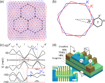
Figure 1(c) shows the moiré band structure calculated for TDBG with , assuming that the middle two graphene layers are coupled by the same sub-lattice and position dependent hybridization as in twisted bilayer graphene Bistritzer and MacDonald (2011, 2010). The -dependent Hamiltonian is then constructed in a plane-wave representation. To be consistent with atomistic calculations that account for strain and out-of-plane relaxation effectsvan Wijk et al. (2015); Jain et al. (2016), we set , where and are respectively the interlayer hopping amplitudes between A and A and between A and B sublattices. The outer two graphene layers are described by the minimal model of Bernal stacked bilayer graphene, considering only the hopping () between dimer sites. We use eV, consistent with infrared spectroscopy studies Zhang et al. (2008); Li et al. (2009). For twists in the 1-1.3° range, the lowest lying conduction and valence bands become relatively flat, which promotes electron-electron interactions and can lead to correlated transport phenomena Cao et al. (2018a, b); Yankowitz et al. (2019); Sharpe et al. (2019); Lu et al. (2019). Figure 1(c) exhibits gaps at neutrality between the lowest conduction and valence bands (), and also gaps within the conduction () and valence () band structures between the first and second (), and third and fourth MBs (). The mechanism responsible for band flatness in TDBG is quite distinct from that in twisted single-layer systems, as explained more fully in the supplemental material.
Our TDBG samples are encapsulated in 20-50 nm thick boron nitride with graphite top and bottom gates [Fig 1(d)]. All layers are mechanically exfoliated, and the TDBG is realized using techniques similar to those described in Kim et al. (2016), with both graphene bilayers originating from the same single crystal and subsequently twisted to a precise angle during the transfer process. The TDBG samples are shaped into Hall bars using reactive ion etching, and independent edge contacts Wang et al. (2013) are made to the active area and gates. We discuss three TDBG samples, with twist angles , , and . The sample has a uniform twist angle to within over a channel length of , while the sample shows a variation in the twist angle of along the channel. The sample did not have a sufficient number of contacts to quantify the angle uniformity.
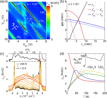
The longitudinal () and Hall () resistivities of the TDBG samples are probed using low frequency lock-in techniques. Our dual gated structure allows top () and bottom () gate voltages to independently tune the carrier density, , and the transverse electric field, , where and are the top and bottom gate capacitances, is the electron charge, and is the vacuum permittivity. Figure 2(a) shows vs and in the 1.01 sample at a temperature . The data show resistivity maxima at the charge neutrality point (CNP), and at a fixed density and 3. Based on Fig. 1(c), which show gaps at neutrality as well as between the the first and second, and third and fourth MBs, we associate with filling of the first MB. Using the four-fold spin and valley degeneracy for each MB state, the wave-length, and therefore the twist angle, can be determined using .
Interestingly, at the CNP increases as a function of -field, while the values at are large at , but decrease with increasing . The resistivity at is relatively constant within the accessible gate voltage range. In addition, we observe resistivity peaks at fractional MB fillings, most notably at half filling of the first conduction band within two small -field windows. The appearance of a gap in a half filled band is a hallmark of strong correlation physics, as demonstrated explicitly in ultra-cold atoms trapped in optical lattices Greiner et al. (2002); Stöferle et al. (2004); Jördens et al. (2008).
To help elucidate the TDBG transport characteristics, we examine the band structure evolution as a function of -field by introducing an on-site energy difference between adjacent layers (), which should be viewed as the external field potential difference corrected for screening; is the graphene layer separation. The screening effect due to induced carriers is non-negligible (see supplemental material), and results in a significant reduction in compared to . Figure 2(b) shows how the gaps introduced in Fig. 1(c) vary with when . behaves like the gap of a single graphene bilayer and increases with Zhang et al. (2009). On the other hand, decreases and vanishes at a finite , while remains relatively constant. For both and , the gaps between valence sub-bands are smaller and tend to zero at lower -fields than for the corresponding conduction sub-bands. A comparison between Fig. 2(a) and 2(b) data shows good qualitative agreement between experiment and calculations, and validates the assignment of to full MB filling, and therefore also the angle extraction from the transport characteristics. Interestingly, the maxima at is observed at -field values that yield insulators at both charge neutrality and , i.e. when . Under this condition, the first conduction band is maximally separated from both of its neighboring bands, suggesting that isolated bands favor the emergence of correlated insulators, and localized mainly in the outside layer that has the highest on-site energy (Fig. S1). This observation is also consistent with the absence of features at half filling in the valence band of Fig. 2(a) data, since and are never large enough at the same -field to sufficiently separate the first valence band from surrounding bands.
In Figures 2(c-d) we examine the temperature dependence of the TDBG. Figure 2(c) shows vs along a horizontal line-cut of Fig. 2(a) data, at , from to . The upper inset shows a zoomed view of the line-cut at in which several developing maxima are observed at half and quarter MB fillings. For densities between the insulators, the temperature dependence is metallic at lower ’s, with increasing with up to , followed by a decrease with increasing . Figure 2(d) shows the -dependence at select densities, indicated by the arrows in Fig 2(c). In the metallic regions the resistivity has a nearly linear dependence on temperature, similar to experimental observations in MATBG Cao et al. (2019a); Polshyn et al. (2019), which has been theoretically attributed either to acoustic phonon scattering in flat bands Wu et al. (2019); Li et al. (2019) or to strong correlation effects Cao et al. (2019a). The decrease in at higher temperatures is attributed to thermal activation to higher bands which are more dispersive and therefore have higher electron velocities Polshyn et al. (2019). We note that exceptionally low values can be observed at certain MB fillings [blue arrow and trace in Fig. 2(c) and 2(d), respectively], which might signal an emerging superconducting state. Figure 2(d) inset shows that the slope of vs. in the linear regions is relatively agnostic to , apart from slight dips indicating emergent insulators at fractional band fillings.
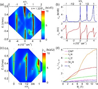
Figure 3(a) shows vs and measured in a TDBG sample with , at K. Similar to the Fig. 2(a) data, single particle gaps appear at charge neutrality and , and correlated insulators arise in a range of positive and negative -fields. The vs. data of the sample is similar to Fig. 2(d) data, showing a linear dependence below , with density dependent values of (Fig. S2). Figure 3(b) shows and vs. measured in a perpendicular magnetic field at [dashed line in Fig 3(a)]. The vs. data changes sign at the single particle and correlated insulators, consistent with a transition between hole-like and electron-like bands when the Fermi level crosses an energy gap, and signaling that the four-fold band degeneracy is lifted in the first conduction MB. As in the Fig. 2 data, the insulators at are present at -field values concomitant with insulating states at both CNP and . However the correlated insulators at are now more prominent, with values similar to those of the single particle insulators.
Band structure calculations offer an explanation for the differences between the and samples (Fig. S3). As a function of -field, the condition provides the maximum separation of the first MB from the neighbouring bands. This separation varies with , and reaches a maximum at . We note that the width of the first conduction band at also increases with . Together the experimental data and calculations suggest that correlated insulators at fractional band fillings are most likely to emerge if the band is maximally separated from neighbouring bands, and that this criterion is more important than extreme band flatness. If only band flatness is considered, correlated insulators should be more prominent at where the lowest bands are narrower. We emphasize again that the mechanism for band flatness in TDBG is different than in the twisted single layer case, and that the band width in TDBG is a less sensitive function of twist angle.
Further insight into the nature of the correlated insulators is provided by measurements in an in-plane magnetic field (), which couples only to the electron spin. Figure 3(c) shows vs and at , and K. Correlated insulators emerge at and in narrower -field windows of . In addition, the insulator at extends over a slightly larger range of -fields. The presence of gaps at each MB quarter filling suggests a full lifting of the four-fold spin and valley degeneracy, in which each electron added per moiré unit cell is polarized in both spin and valley. Figure 3(d) shows normalized to its zero field value () vs. at different MB fillings. At and , grows rapidly with , whereas the growth is more gradual at . Figure 3(c-d) data suggest the insulators at and are spin polarized, with gaps enhanced by the applied , and correspondingly that the insulator at is valley polarized.
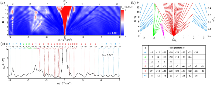
We also consider the effect of a magnetic field perpendicular to the sample plane. Electrons in a periodic potential and perpendicular magnetic field develop a self-similar energy spectrum known as Hofstadter’s butterfly Hofstadter (1976), which has been studied extensively in graphene/boron nitride moiré patterns Ponomarenko et al. (2013); Dean et al. (2013); Hunt et al. (2013); Yu et al. (2013), and in twisted bilayer graphene Cao et al. (2016); Kim et al. (2017); Cao et al. (2018a, b); Yankowitz et al. (2019); Lu et al. (2019). In such systems, quantum Hall states (QHSs), indexed by a Landau level filling factor () and a sub-band filling factor (), emerge when ; is the electron charge and is Planck’s constant. Figure 4(a) shows a contour plot of vs. and measured in a TDBG sample with , at . The data shows QHS fans corresponding to , with emerging fans at , and . While the values are predominately multiples of four, the fan shows minima at single integer filling factors, which indicates a lifting of the Landau level spin and valley degeneracy, as well as unexpected states at and [Fig. 4(b)]. In Fig. 4(c) we show a line-cut of Fig. 4(a) along where the various minima are labeled according to MB and . At high fields, the fan exhibits minima corresponding to (Fig. S4). It is also interesting to examine the fan intersections. For example, where the and fans meet, only the minima from the fan persists while all others are suppressed. A similar behavior is observed for . This may point towards topological distinctions between the different moiré bands or Landau levels Lian et al. (2018).
We have presented a study of electrical transport in twisted double bilayer graphene, a system that exhibits single particle gaps in the moire band spectrum along with correlated insulators at half and quarter fillings of the first conduction band. A combination of theoretical and experimental data suggests that correlated insulators are most likely to occur in a band when it is maximally separated from neighbouring bands. Measurements in an in-plane magnetic field indicate that the correlated insulators are predominantly spin polarized at 1/4 and 3/4 fillings, and valley polarized at 1/2 filling.
Acknowledgements.
This work was supported by the National Science Foundation grants EECS-1610008 and DMR-1720595, Army Research Office under Award W911NF-17-1-0312, and the Welch Foundation. Work was partly done at the Texas Nanofabrication Facility supported by NSF grant NNCI-1542159. K.W. and T.T. acknowledge support from the Elemental Strategy Initiative conducted by the MEXT, Japan and JSPS KAKENHI Grant Numbers JP15K21722.Note added.—During the preparation of this manuscript we became aware of two related studies Liu et al. (2019); Cao et al. (2019b).
References
- Bistritzer and MacDonald (2011) R. Bistritzer and A. H. MacDonald, Proc. Natl. Acad. Sci. U.S.A. 108, 12233 (2011).
- Suárez Morell et al. (2010) E. Suárez Morell, J. D. Correa, P. Vargas, M. Pacheco, and Z. Barticevic, Phys. Rev. B 82, 121407 (2010).
- Kim et al. (2016) K. Kim, M. Yankowitz, B. Fallahazad, S. Kang, H. C. P. Movva, S. Huang, S. Larentis, C. M. Corbet, T. Taniguchi, K. Watanabe et al., Nano Lett. 16, 1989 (2016).
- Cao et al. (2016) Y. Cao, J. Luo, V. Fatemi, S. Fang, J. Sanchez-Yamagishi, K. Watanabe, T. Taniguchi, E. Kaxiras, and P. Jarillo-Herrero, Phys. Rev. Lett. 117, 116804 (2016).
- Kim et al. (2017) K. Kim, A. DaSilva, S. Huang, B. Fallahazad, S. Larentis, T. Taniguchi, K. Watanabe, B. J. LeRoy, A. H. MacDonald, and E. Tutuc, Proc. Natl. Acad. Sci. U.S.A. 114, 3364 (2017).
- Cao et al. (2018a) Y. Cao, V. Fatemi, A. Demir, S. Fang, S. L. Tomarken, J. Y. Luo, J. D. Sanchez-Yamagishi, K. Watanabe, T. Taniguchi, E. Kaxiras et al., Nature 556, 80 (2018a).
- Cao et al. (2018b) Y. Cao, V. Fatemi, S. Fang, K. Watanabe, T. Taniguchi, E. Kaxiras, and P. Jarillo-Herrero, Nature 556, 43 (2018b).
- Yankowitz et al. (2019) M. Yankowitz, S. Chen, H. Polshyn, Y. Zhang, K. Watanabe, T. Taniguchi, D. Graf, A. F. Young, and C. R. Dean, Science 363, 1059 (2019).
- Lu et al. (2019) X. Lu, P. Stepanov, W. Yang, M. Xie, M. A. Aamir, I. Das, C. Urgell, K. Watanabe, T. Taniguchi, G. Zhang et al., arXiv:1903.06513 [cond-mat] (2019).
- McCann and Fal’ko (2006) E. McCann and V. I. Fal’ko, Phys. Rev. Lett. 96, 086805 (2006).
- Zhang et al. (2009) Y. Zhang, T.-T. Tang, C. Girit, Z. Hao, M. C. Martin, A. Zettl, M. F. Crommie, Y. R. Shen, and F. Wang, Nature 459, 820 (2009).
- Bistritzer and MacDonald (2010) R. Bistritzer and A. H. MacDonald, Phys. Rev. B 81, 245412 (2010).
- van Wijk et al. (2015) M. M. van Wijk, A. Schuring, M. I. Katsnelson, and A. Fasolino, 2D Mater. 2, 034010 (2015).
- Jain et al. (2016) S. K. Jain, V. Juričić, and G. T. Barkema, 2D Mater. 4, 015018 (2016).
- Zhang et al. (2008) L. M. Zhang, Z. Q. Li, D. N. Basov, M. M. Fogler, Z. Hao, and M. C. Martin, Phys. Rev. B 78, 235408 (2008).
- Li et al. (2009) Z. Q. Li, E. A. Henriksen, Z. Jiang, Z. Hao, M. C. Martin, P. Kim, H. L. Stormer, and D. N. Basov, Phys. Rev. Lett. 102, 037403 (2009).
- Sharpe et al. (2019) A. L. Sharpe, E. J. Fox, A. W. Barnard, J. Finney, K. Watanabe, T. Taniguchi, M. A. Kastner, and D. Goldhaber-Gordon, arXiv:1901.03520 [cond-mat] (2019).
- Wang et al. (2013) L. Wang, I. Meric, P. Y. Huang, Q. Gao, Y. Gao, H. Tran, T. Taniguchi, K. Watanabe, L. M. Campos, D. A. Muller et al., Science 342, 614 (2013).
- Greiner et al. (2002) M. Greiner, O. Mandel, T. Esslinger, T. W. Hänsch, and I. Bloch, Nature 415, 39 (2002).
- Stöferle et al. (2004) T. Stöferle, H. Moritz, C. Schori, M. Köhl, and T. Esslinger, Phys. Rev. Lett. 92, 130403 (2004).
- Jördens et al. (2008) R. Jördens, N. Strohmaier, K. Günter, H. Moritz, and T. Esslinger, Nature 455, 204 (2008).
- Cao et al. (2019a) Y. Cao, D. Chowdhury, D. Rodan-Legrain, O. Rubies-Bigordá, K. Watanabe, T. Taniguchi, T. Senthil, and P. Jarillo-Herrero, arXiv:1901.03710 [cond-mat] (2019a).
- Polshyn et al. (2019) H. Polshyn, M. Yankowitz, S. Chen, Y. Zhang, K. Watanabe, T. Taniguchi, C. R. Dean, and A. F. Young, arXiv:1902.00763 [cond-mat] (2019).
- Wu et al. (2019) F. Wu, E. Hwang, and S. Das Sarma, Phys. Rev. B 99, 165112 (2019).
- Li et al. (2019) X. Li, F. Wu, and S. D. Sarma, arXiv:1906.08224 [cond-mat] (2019).
- Hofstadter (1976) D. R. Hofstadter, Phys. Rev. B 14, 2239 (1976).
- Ponomarenko et al. (2013) L. A. Ponomarenko, R. V. Gorbachev, G. L. Yu, D. C. Elias, R. Jalil, A. A. Patel, A. Mishchenko, A. S. Mayorov, C. R. Woods, J. R. Wallbank et al., Nature 497, 594 (2013).
- Dean et al. (2013) C. R. Dean, L. Wang, P. Maher, C. Forsythe, F. Ghahari, Y. Gao, J. Katoch, M. Ishigami, P. Moon, M. Koshino et al., Nature 497, 598 (2013).
- Hunt et al. (2013) B. Hunt, J. D. Sanchez-Yamagishi, A. F. Young, M. Yankowitz, B. J. LeRoy, K. Watanabe, T. Taniguchi, P. Moon, M. Koshino, P. Jarillo-Herrero et al., Science 340, 1427 (2013).
- Yu et al. (2013) G. L. Yu, R. V. Gorbachev, J. S. Tu, A. V. Kretinin, Y. Cao, R. Jalil, F. Withers, L. A. Ponomarenko, B. A. Piot, M. Potemski et al., Nat. Phys. 10, 525 (2014).
- Lian et al. (2018) B. Lian, F. Xie, and B. A. Bernevig, arXiv:1811.11786 [cond-mat] (2018).
- Liu et al. (2019) X. Liu, Z. Hao, E. Khalaf, J. Y. Lee, K. Watanabe, T. Taniguchi, A. Vishwanath, and P. Kim, arXiv:1903.08130 [cond-mat] (2019).
- Cao et al. (2019b) Y. Cao, D. Rodan-Legrain, O. Rubies-Bigorda, J. M. Park, K. Watanabe, T. Taniguchi, and P. Jarillo-Herrero, arXiv:1903.08596 [cond-mat] (2019b).
I Supplemental Material:
Correlated Insulating States in Twisted Double Bilayer Graphene
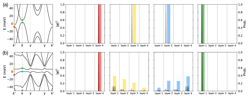
In TDBG, the mechanism of flat band formation is different from that of TBG, as noted in the main text. The nature of the low energy bands can be understood qualitatively by first considering the limit in which the inner two graphene layers, the layers which have a relative twist, are decoupled. As illustrated in Fig. S1(a), the low-energy states at the moiré Brillouin zone (MBZ) corners are then localized on individual layers from 1 to layer 4, and on the honeycomb sub-lattice in that layer which does not have a near-neighbor in the same bilayer. The energies at the MBZ corners are , , and respectively, where is the on-site energy difference between adjacent layers. While in TBG, low-energy states localize on both sub-lattices of each layer. The color-coded bars (-label on the right) in Fig S1 give the layer-dependent probability distributions for the corresponding high-symmetry -points in the MBZ marked by colored points in the band structure. When the inner layers are then coupled, level repulsion tends to push the energies of states with high weight in these layers to high energies. The interplay between sublattice-coupling within layers and sublattice-dependent interlayer tunneling which yields the magic angle flat bands in bilayers does not take place because only one sublattice is available in each layer at low energies. This leaves low energy bands that are dominantly localized in the outer two layers, as illustrated in Fig. S1(b).
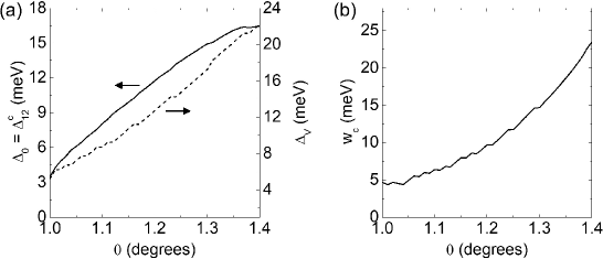
At , the screened potential energy difference between two adjacent graphene layers is , where nm, and the superlattice density cm-2 for . Using a relative permittivity of twisted bilayer graphene of /citenamefont Chung et!al. (2018) leads to a screened potential energy meV.
References
- /citenamefont Chung et!al. (2018) T. F. Chung, Y. Xu, Y. P. Chen, Phys. Rev. B 98, 035425 (2018).