Present address: ] Dept. of Electrical & Electronic Engineering, Univ. of Dhaka, Dhaka 1000, Bangladesh
Present address: ] Massachusetts Institute of Technology, Cambridge, MA 02139, USA
Fast gate-based readout of silicon quantum dots using Josephson parametric amplification
Abstract
Spins in silicon quantum devices are promising candidates for large-scale quantum computing. Gate-based sensing of spin qubits offers compact and scalable readout with high fidelity, however further improvements in sensitivity are required to meet the fidelity thresholds and measurement timescales needed for the implementation of fast-feedback in error correction protocols. Here, we combine radio-frequency gate-based sensing at 622 MHz with a Josephson parametric amplifier (JPA), that operates in the 500–800 MHz band, to reduce the integration time required to read the state of a silicon double quantum dot formed in a nanowire transistor. Based on our achieved signal-to-noise ratio (SNR), we estimate that singlet-triplet single-shot readout with an average fidelity of 99.7% could be performed in 1 s, well-below the requirements for fault-tolerant readout and 30 times faster than without the JPA. Additionally, the JPA allows operation at a lower RF power while maintaining identical SNR. We determine a noise temperature of 200 mK with a contribution from the JPA (25%), cryogenic amplifier (25%) and the resonator (50%), showing routes to further increase the read-out speed.
Quantum computers require high-fidelity qubit measurement, which must be performed on a timescale faster than the decoherence time to perform quantum error correction Fowler et al. (2012). Spin qubits formed in quantum dots (QDs) or donors in silicon are one of the most promising platforms for scalable quantum information processing due to their long coherence times and large integration density Vandersypen et al. (2017); Veldhorst et al. (2017); Li et al. (2018); Pica et al. (2016); Hill et al. (2015); Cai et al. (2019). In such devices, readout has been typically achieved using nearby electrometers to detect the spin state via spin-to-charge conversion based on spin dependent tunneling Elzerman et al. (2004); Morello et al. (2010) or Pauli spin blockade Prance et al. (2012); Barthel et al. (2009); Zhao et al. (2018), with radio-frequency (RF) single-electron transistors being the most sensitive electrometers to date Schoelkopf (1998); Brenning et al. (2006). When scaling to large arrays of dense qubits Jones et al. (2018); Veldhorst et al. (2017); Vandersypen et al. (2017); Li et al. (2018) space for additional electrometers and reservoirs is limited: Gate-based dispersive RF readout eliminates the need for additional sensor structures Colless et al. (2013); Gonzalez-Zalba et al. (2015); Petersson et al. (2010) and reservoirs (using Pauli spin blockade) Schroer et al. (2012); Betz et al. (2015); Urdampilleta et al. (2015) by embedding the gates that define the quantum dot into a resonant circuit. This gate-based readout relies on detecting a shift in the phase of the RF signal reflected by the resonator which is proportional to the quality factor (), the square of the gate coupling and the inverse of the total capacitance of the resonator Ahmed et al. (2018). Recently, single-shot readout of the singlet-triplet states in a double QD has been demonstrated with gate-based sensors, using a variety of resonator parameters to achieve a range of readout fidelities (for a given integration time): (2.6 ms) West et al. (2019), (s) Pakkiam et al. (2018), (s) Zheng et al. (2019) to (1 ms; using ancillary ‘sensor’ QD and reservoir) Urdampilleta et al. (2018).
Amplifiers based on Josephson junctions have greatly improved signal-to-noise ratios (SNRs) in the field of superconducting circuits Slichter et al. (2016); Vijay et al. (2012, 2011); Eichler et al. (2012); Chen et al. (2012); Hatridge et al. (2011) — they typically operate at frequencies of several GHz and near the quantum limit of noise introduced by the amplifier (or indeed below, for a single quadrature using squeezing) Caves et al. (2012); Castellanos-Beltran et al. (2008); Castellanos-Beltran and Lehnert (2007); Eichler et al. (2011); Bergeal et al. (2010); Macklin et al. (2015). Adopting such approaches in the measurement of QDs at RF/microwave frequencies is expected to lead to corresponding improvements in SNR. While this can in principle be achieved at operating frequencies of 4–8 GHz that are typical for Josephson-junction based amplifiers, as demonstrated using an InAs double QD, Josephson parametric amplifier (JPA) and coplanar waveguide resonator Stehlik et al. (2015), lower frequency operation ( GHz) becomes necessary 111operating at a frequency comparable to the tunnel coupling results in back-action of the resonator onto the quantum dot device in form of fast voltage oscillations that manifest as Landau-Zener transitions for studying lower QD tunneling rates, at which exchange interaction is more easily controlled, and for enabling off-chip resonator fabrication. Suitable amplifiers are available in such a frequency range, for example: a JPA operating at 600 MHz with a noise temperature of mK Simbierowicz et al. (2018) or a SQUID amplifier chain with mK at 538 MHz Mück et al. (2001). Building on such developments, readout of a GaAs based quantum dot at 196 MHz with a noise temperature of 490 mK was recently reported using a SQUID amplifier Schupp et al. (2018).
In this Letter, we combine RF capacitive gate-based sensing of silicon QDs with Josephson parametric amplification to push the bounds of SNR that can be achieved using this technique. We use a well-matched lumped-element high resonator containing a NbN spiral inductor and a JPA that operates in the 500–800 MHz band and obtain an overall noise temperature mK at 621.9 MHz. We benchmark the sensitivity of the method using electronic transitions in a silicon multi-dot device with large gate-coupling (wrap-around geometry) fabricated following CMOS processes. When using the JPA at an inter-dot charge transition, we find an improvement of a factor of 7 in the SNR and a minimum integration time of 80 ns. Based on our measurements, we estimate an average single-shot fidelity of would be possible in s without the JPA, yet only s with the JPA. These improvements in readout speed enable implementations of error correction codes and fast feedback for silicon-based quantum devices.
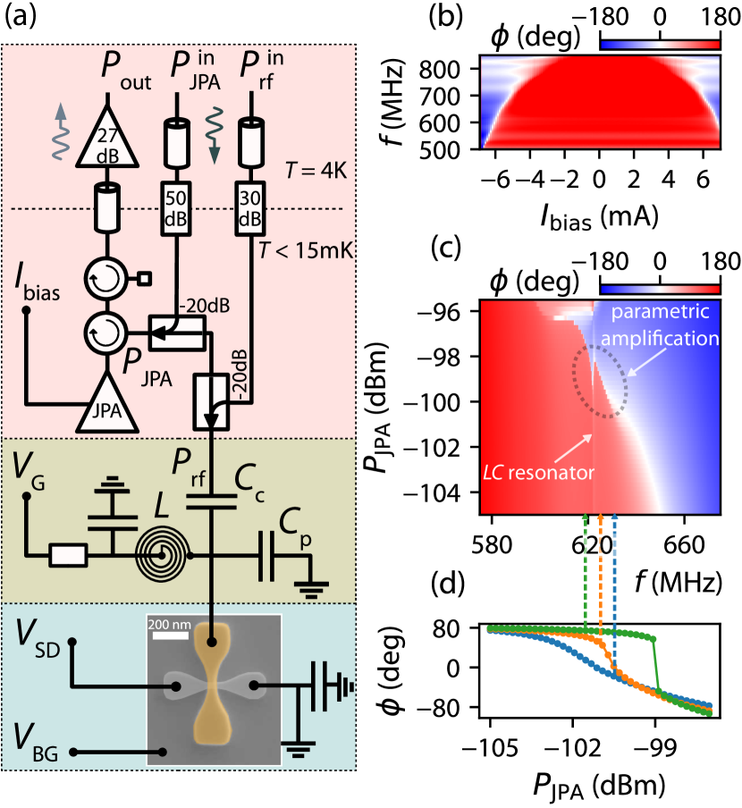
A schematic of how the JPA is embedded into the cryogenic reflectometry setup is shown in Fig. 1(a). The setup consists of i) the cryogenic RF delivery and amplification chain including the JPA (pink background); ii) a lumped-element resonator (green); and iii) the silicon quantum dot device (blue), see Sup for details. In gate-based sensing, the device is embedded in a resonator which is probed using an RF tone with power at resonant frequency . At this frequency, changes in device capacitance, , due to cyclic single-electron tunneling produce changes in the reflection coefficient Mizuta et al. (2017). This effect translates into a change in the reflected power with an SNR given by
where is the noise power. The optimal SNR is achieved by maximizing (i.e. large loaded quality factor and small parasitic capacitance, which translates into a large resonator impedance, combined with large gate coupling and a well matched resonator) Ahmed et al. (2018), maximizing (while remaining below power broadening) and minimizing .
The noise power for an amplifier with gain can be defined as where and are the system and amplifier noise temperature (noise added by the amplifier) respectively, is Boltzmann’s constant and is the amplifier bandwidth. In semiconductor QD measurements, cryogenic high electron mobility transistor (HEMT) amplifiers operating at 4 K typically limit the effective noise temperature () to a few Kelvin. By including an additional amplifier (such as a JPA) with gain and lower noise temperature () at the beginning of the amplification chain, the effective noise temperature can be reduced:
| (1) |
For a JPA operating at mK we expect a minimum of mK.
As shown in Fig. 1(a), the RF signal reflected from the quantum device passes the JPA (which works in reflection) via a circulator and is further amplified at K followed by additional amplification and quadrature demodulation for measurement at room temperature (not shown). Our JPA is a low quality factor () superconducting resonator consisting of a SQUID loop array with tunable inductance shunted by a fixed capacitance Vijay et al. (2009), and is tunable in frequency from 500–800 MHz, as shown in Fig. 1(b), by passing a current through a coil that changes the flux through the nearby SQUIDs. The JPA is pumped via the signal input port and with power , delivered using a separate microwave line. At low drive power the JPA behaves like a linear resonator, while at high power the non-linearity of the Josephson junctions manifests in a frequency shift of the JPA to lower frequency until eventually the JPA reaches a bi-stable regime Vijay et al. (2009). The JPA phase response as a function of pump power and frequency is shown in Fig. 1(c) where the additional phase shift originating from the resonator and the regime useful for parametric amplification are indicated. In this regime, the phase of the reflected pump signal varies rapidly with the pump power, as shown in Fig. 1(d), which represents the transfer function of the JPA. When biased at this point, changes in the pump amplitude due to a small signal lead to large changes in the reflected phase, such that the gain is determined by the gradient of the transfer function while the width in power sets the dynamic range. For small modulations of , the response is linear.
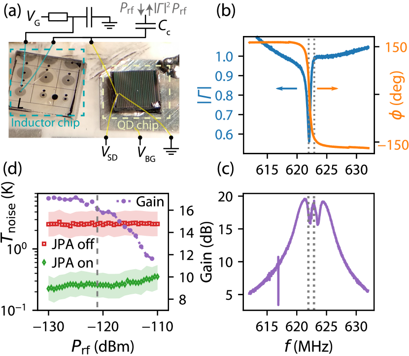
The dynamic range of this JPA is of the order of dBm, making it unsuitable for the signal powers commonly used in previous reflectometry measurements ( to dBm) Gonzalez-Zalba et al. (2015). Here, we overcome this limitation using a high quality factor resonator that is well coupled to the input line. The high -factor enables a reduced RF signal power to be used while achieving the same gate voltage on the device. The resonator circuit is formed by the parallel combination of a NbN spiral inductor nH, parasitic capacitance and the quantum dot device ( fF), all coupled to the RF line via a coupling capacitor ( fF). We observe a resonance in the reflection coefficient at MHz with a loaded quality factor of , impedance , return loss of 3 dB and phase shift (over-coupled) as shown in Fig. 2(b). When operating at a charge instability in the QD device, the resonator reaches perfect matching. We operate the JPA in phase-preserving mode, where there is an offset between the JPA pump frequency () and , so power from the JPA pump is transferred onto and (four-wave mixing) via double-sideband phase modulation as illustrated by the transfer function. We select MHz to fall between the bandwidth of the resonator MHz and the JPA MHz. This puts at the edge of the readout resonator to avoid power broadening due to leakage of the pump signal while maximizing gain at . When tuned and pumped, we achieve a gain of 17 dB at as shown in Fig. 2(c). The decrease in gain near is likely due to large impedance variations of the resonator close to resonance and imperfect matching to 50 .
Figure 2(d) shows the JPA gain and the effective noise temperature close to as a function of . We identify 1-dB-compression at dBm. Based on amplifier gain estimations ( dB) we obtain an effective noise temperature K with the JPA off (consistent with the cryogenic amplifier specifications) and a minimum noise temperature of mK based on the SNR improvement with the JPA on. The effective noise temperature with the JPA on increases with increasing power due to saturation. There are multiple contributions to , captured in Eq. 1. We calculate the contribution of the cryogenic amplifier mK and estimate and by comparing when operating the QD device away from or at a charge instability. can have contributions from the resonator circuit () and the QD device (): Müller et al. (2013), where is the fraction of the rf power dissipated in the device. As we shall see later, in our device, tunneling between the QD and reservoir occurs adiabatically and hence . Based on an increase in of mK when operating at a charge transition (where decreases from to ), we estimate mK and mK. We relate to an electron temperature of dissipative elements in the resonant circuit and a we note that a JPA efficiency of 36% of the quantum limit (equivalent to photons) is compatible with previous results for operation close to a bifurcation point Bryant et al. (1991); Hatridge et al. (2011); Boutin et al. (2017).
Next, we characterize and compare the improvements in the SNR of gate-based readout using a quantum dot-to-reservoir transition (DRT) and inter-dopant/dot charge transition (IDT) in a CMOS silicon nanowire field-effect transistor device with channel width and gate length of 30 nm and nanowire height of 11 nm Urdampilleta et al. (2015). Figure 3(a) shows a schematic line-cut of the device along the gate (see SEM micro-graph in Fig. 1(a)). QDs form in the corners of the device and have a strong coupling to the gate . Additionally, given the doping density, an average of 5 (phosphorus) donors are expected in the device channel Urdampilleta et al. (2015).
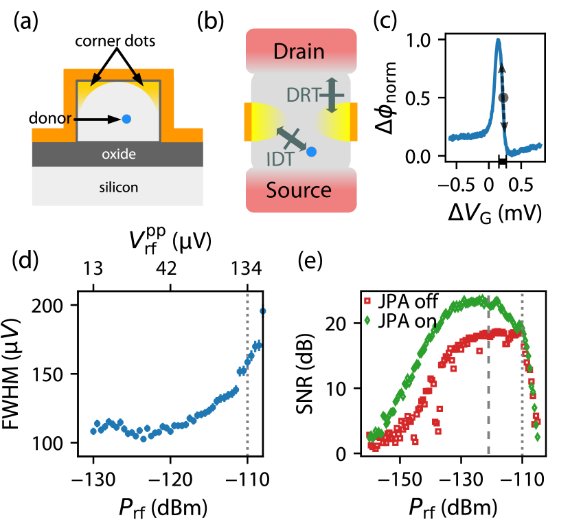
We first focus on a DRT transition in the device, in which a QD is primarily tunnel coupled to the drain reservoir as illustrated in a schematic line-cut of the device along the source-drain direction in Fig. 3(b). When operating at the DRT transition we observe a capacitive shift of the resonance corresponding to fF. In Fig. 3(d) we show the full-width half maximum of the selected transition as a function of . No power broadening is observed for below dBm, while the transition is significantly broadened above dBm. Due to the high of the resonator, only a small input power, compatible with the dynamic range and saturation of the JPA, is required and we calculate the RF disturbance at the device gate as , corresponding, for example, to V for an input RF power of dBm.
Next, we use conventional methods to measure the charge sensitivity Sup ; Schoelkopf (1998) with and without the JPA, which provides a device-specific benchmark on the performance of our gate-based sensor normalized to the gate charge. The SNR as a function of , with and without the JPA, is shown in Fig. 3(e), when operating at a small gate voltage modulation of 50 kHz as indicated in Fig. 3(c). We observe an improvement of up to 8 dB in SNR with the JPA at low RF power. Irrespective of whether the JPA is used, for between and dBm the SNR levels off as DRT begins to become power broadened, and it drops abruptly for powers above dBm. With the JPA on there is an additional decrease in SNR evident above dBm as the JPA saturates. The JPA can either be used to increase the SNR beyond what could otherwise be achieved, and/or to provide the same SNR but at about 10 dB less RF power, with the corresponding reduction in the disturbance of the QD being measured, and its neighbors. When operating well below power broadening ( dBm), the charge sensitivity achieved with the JPA is compared to without the JPA, outperforming previous measurements using RF-SET Brenning et al. (2006) and gate-based approaches Ahmed et al. (2018).
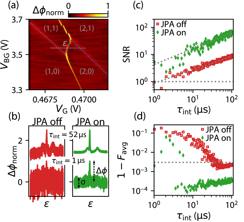
Finally, we move on to benchmark the readout using a donor-dot IDT of even parity Sup that exhibits features of spin blockade Schroer et al. (2012). Figure 4(a) shows the IDT in the normalized phase response as a function of and back-gate voltage (), where the donor transition can be identified due to a stronger coupling to (donor resides deeper in the channel, closer to the back-gate). We determined the charge occupation of the donor and QD (up to an arbitrary offset) using the magnetic field response and we calculate a gate coupling and tunnel coupling eV, corresponding to a capacitive shift of fF Sup . Figure 4(b) shows an example of the phase response across the IDT, along the detuning axis shown in Fig. 4(a) for s and s. We determine the power SNR from the amplitude of the IDT signal and the RMS amplitude of the noise as . Figure 4(c) shows the SNR as a function of integration time with the JPA on and off. We observe an improvement in SNR of a factor of 7 with the JPA on consistent with the SNR improvement of 8 dB observed in the charge sensitivity measurement. Using an extrapolation (dotted lines in Fig. 4(c)) we infer an SNR of unity at s and ns with the JPA off and on, respectively. However, the limited bandwidth of our resonator prohibits measurements faster than s ( MHz). Additionally, we observe that multiple measurements of the SNR with the JPA on for s deviate from the extrapolation, which could be due to noise introduced by the JPA pump signal which is operated only 1 MHz offset the RF signal. Based on the signal and noise levels (as shown in Fig. 4(c)) we simulate the singlet and triplet readout probability densities Sup , modeled as two noise-broadened Gaussian distributions Barthel et al. (2009). The model includes terms to account for relaxation of the triplet during measurement and we assume ms West et al. (2019). From the probability densities we obtain an average readout infidelity as a function of integration time which is shown Fig. 4(d) for the JPA off and on. We find that can be reached at a corresponding to an integration time of at least s with the JPA off and s with the JPA on allowing readout faster than the the coherence time of electron spins in 28Si ( s Veldhorst et al. (2014)).
We have demonstrated that the SNR of RF gate-based readout of quantum dot devices can be improved using a JPA. We observe a SNR improvement of 8 dB for both dot-to-reservoir and inter-donor/dot transitions when the JPA is operated closed to the RF frequency in phase-preserving mode at 17 dB gain. We have analyzed the performance of the JPA in an external magnetic field, commonly applied in spin qubit devices, and find no disturbance on the JPA performance up to a field of T at the device Sup . The SNR improvement we see is currently limited by the gain of the JPA, yielding a contribution of the cryogenic amplifier of at least 50 mK to the system noise temperature. Assuming a JPA gain of 23 dB or more, the contribution of the cryogenic amplifier would become negligible. The system noise performance could be further improved by operating the JPA in phase-sensitive mode, where the noise added by the JPA can be squeezed below the quantum limit. Changes in the circuit such as additional isolators between the JPA and readout resonator as well as additional line attenuation and filtering could be beneficial towards achieving larger gain, a lower system noise temperatures and prevent leakage of the JPA pump signal into the readout resonator. In addition, the measurement speed in this implementation is, in principle, limited by the bandwidth of our high- readout resonator: increasing the coupling to the line or, preferentially, moving to a higher frequency of the resonator circuit while maintaining high loaded should allow sub-microsecond fault-tolerant gate-based spin readout. Further development could reduce the footprint of the high resonators, to achieve an integrated and scalable readout architecture Schaal et al. (2019) with the potential of reduced circuit losses and parasitics. Using a traveling wave parametric amplifier (TWPA) with increased bandwidth, frequency multiplexing of multiple resonators could be achieved.
Acknowledgements.
This research has received funding from the European Union’s Horizon 2020 research and innovation programme under grant agreement No 688539 (http://mos-quito.eu) and Seventh Framework Programme (FP7/2007-2013) through Grant Agreement No. 318397 (http://www.tolop.eu.); as well as by the Engineering and Physical Sciences Research Council (EPSRC) through the Centre for Doctoral Training in Delivering Quantum Technologies (EP/L015242/1), UNDEDD (EP/K025945/1) and QUES2T (EP/N015118/1). J.W.A.R. acknowledges funding from the EPSRC through International Network and Programme Grants (EP/P026311/1; EP/N017242/1). JPA development was supported by the Army Research Office under Grant No. W911NF-14-1-0078. M.F.G.Z. acknowledge support from the Royal Society and Winton Programme for the Physics of Sustainability.References
- Fowler et al. (2012) A. G. Fowler, M. Mariantoni, J. M. Martinis, and A. N. Cleland, Physical Review A 86, 032324 (2012) .
- Vandersypen et al. (2017) L. M. K. Vandersypen, H. Bluhm, J. S. Clarke, A. S. Dzurak, R. Ishihara, A. Morello, D. J. Reilly, L. R. Schreiber, and M. Veldhorst, npj Quantum Information 3, 34 (2017) .
- Veldhorst et al. (2017) M. Veldhorst, H. G. J. Eenink, C. H. Yang, and A. S. Dzurak, Nature Communications 8, 1766 (2017) .
- Li et al. (2018) R. Li, L. Petit, D. P. Franke, J. P. Dehollain, J. Helsen, M. Steudtner, N. K. Thomas, Z. R. Yoscovits, K. J. Singh, S. Wehner, L. M. K. Vandersypen, J. S. Clarke, and M. Veldhorst, Science Advances 4, eaar3960 (2018) .
- Pica et al. (2016) G. Pica, B. W. Lovett, R. N. Bhatt, T. Schenkel, and S. A. Lyon, Physical Review B 93, 035306 (2016) .
- Hill et al. (2015) C. D. Hill, E. Peretz, S. J. Hile, M. G. House, M. Fuechsle, S. Rogge, M. Y. Simmons, and L. C. L. Hollenberg, Science Advances 1, e1500707 (2015).
- Cai et al. (2019) Z. Cai, M. A. Fogarty, S. Schaal, S. Patomaki, S. C. Benjamin, and J. J. L. Morton, arXiv preprint 1904.10378 (2019) .
- Elzerman et al. (2004) J. M. Elzerman, R. Hanson, L. H. Willems van Beveren, B. Witkamp, L. M. K. Vandersypen, and L. P. Kouwenhoven, Nature 430, 431 (2004) .
- Morello et al. (2010) A. Morello, J. J. Pla, F. a. Zwanenburg, K. W. Chan, K. Y. Tan, H. Huebl, M. Möttönen, C. D. Nugroho, C. Yang, J. a. van Donkelaar, A. D. C. Alves, D. N. Jamieson, C. C. Escott, L. C. L. Hollenberg, R. G. Clark, and A. S. Dzurak, Nature 467, 687 (2010).
- Prance et al. (2012) J. R. Prance, Z. Shi, C. B. Simmons, D. E. Savage, M. G. Lagally, L. R. Schreiber, L. M. K. Vandersypen, M. Friesen, R. Joynt, S. N. Coppersmith, and M. A. Eriksson, Physical Review Letters 108, 046808 (2012).
- Barthel et al. (2009) C. Barthel, D. J. Reilly, C. M. Marcus, M. P. Hanson, and A. C. Gossard, Physical Review Letters 103, 160503 (2009).
- Zhao et al. (2018) R. Zhao, T. Tanttu, K. Y. Tan, B. Hensen, K. W. Chan, J. C. C. Hwang, R. C. C. Leon, C. H. Yang, W. Gilbert, F. E. Hudson, K. M. Itoh, A. A. Kiselev, T. D. Ladd, A. Morello, A. Laucht, and A. S. Dzurak, arXiv preprint 1812.08347 (2018).
- Schoelkopf (1998) R. J. Schoelkopf, Science 280, 1238 (1998).
- Brenning et al. (2006) H. Brenning, S. Kafanov, T. Duty, S. Kubatkin, and P. Delsing, Journal of Applied Physics 100 (2006), 10.1063/1.2388134.
- Jones et al. (2018) C. Jones, M. A. Fogarty, A. Morello, M. F. Gyure, A. S. Dzurak, and T. D. Ladd, Physical Review X 8, 021058 (2018).
- Colless et al. (2013) J. I. Colless, A. C. Mahoney, J. M. Hornibrook, A. C. Doherty, H. Lu, A. C. Gossard, and D. J. Reilly, Physical Review Letters 110, 046805 (2013).
- Gonzalez-Zalba et al. (2015) M. F. Gonzalez-Zalba, S. Barraud, a. J. Ferguson, and a. C. Betz, Nature Communications 6, 6084 (2015).
- Petersson et al. (2010) K. D. Petersson, C. G. Smith, D. Anderson, P. Atkinson, G. A. C. Jones, and D. A. Ritchie, Nano Letters 10, 2789 (2010).
- Schroer et al. (2012) M. D. Schroer, M. Jung, K. D. Petersson, and J. R. Petta, Physical Review Letters 109, 166804 (2012).
- Betz et al. (2015) A. C. Betz, R. Wacquez, M. Vinet, X. Jehl, A. L. Saraiva, M. Sanquer, A. J. Ferguson, and M. F. Gonzalez-Zalba, Nano Letters 15, 4622 (2015).
- Urdampilleta et al. (2015) M. Urdampilleta, A. Chatterjee, C. C. Lo, T. Kobayashi, J. Mansir, S. Barraud, A. C. Betz, S. Rogge, M. F. Gonzalez-Zalba, and J. J. L. Morton, Physical Review X 5, 031024 (2015).
- Ahmed et al. (2018) I. Ahmed, J. A. Haigh, S. Schaal, S. Barraud, Y. Zhu, C.-m. Lee, M. Amado, J. W. A. Robinson, A. Rossi, J. J. L. Morton, and M. F. Gonzalez-Zalba, Physical Review Applied 10, 014018 (2018).
- West et al. (2019) A. West, B. Hensen, A. Jouan, T. Tanttu, C.-H. Yang, A. Rossi, M. F. Gonzalez-Zalba, F. Hudson, A. Morello, D. J. Reilly, and A. S. Dzurak, Nature Nanotechnology (2019), 10.1038/s41565-019-0400-7.
- Pakkiam et al. (2018) P. Pakkiam, A. V. Timofeev, M. G. House, M. R. Hogg, T. Kobayashi, M. Koch, S. Rogge, and M. Y. Simmons, Physical Review X 8, 041032 (2018).
- Zheng et al. (2019) G. Zheng, N. Samkharadze, M. L. Noordam, N. Kalhor, D. Brousse, A. Sammak, G. Scappucci, and L. M. K. Vandersypen, Nature Nanotechnology (2019), 10.1038/s41565-019-0488-9.
- Urdampilleta et al. (2018) M. Urdampilleta, D. J. Niegemann, E. Chanrion, B. Jadot, C. Spence, P.-A. Mortemousque, . C. Bäuerle, L. Hutin, B. Bertrand, S. Barraud, R. Maurand, M. Sanquer, X. Jehl, S. De Franceschi, M. Vinet, and T. Meunier, arXiv preprint 1809.04584 (2018).
- Slichter et al. (2016) D. H. Slichter, C. Müller, R. Vijay, S. J. Weber, A. Blais, and I. Siddiqi, New Journal of Physics 18, 053031 (2016).
- Vijay et al. (2012) R. Vijay, C. Macklin, D. H. Slichter, S. J. Weber, K. W. Murch, R. Naik, A. N. Korotkov, and I. Siddiqi, Nature 490, 77 (2012).
- Vijay et al. (2011) R. Vijay, D. H. Slichter, and I. Siddiqi, Physical Review Letters 106, 110502 (2011).
- Eichler et al. (2012) C. Eichler, C. Lang, J. M. Fink, J. Govenius, S. Filipp, and A. Wallraff, Physical Review Letters 109, 240501 (2012).
- Chen et al. (2012) Y. Chen, D. Sank, P. O’Malley, T. White, R. Barends, B. Chiaro, J. Kelly, E. Lucero, M. Mariantoni, A. Megrant, C. Neill, A. Vainsencher, J. Wenner, Y. Yin, A. N. Cleland, and J. M. Martinis, Applied Physics Letters 101, 182601 (2012).
- Hatridge et al. (2011) M. Hatridge, R. Vijay, D. H. Slichter, J. Clarke, and I. Siddiqi, Physical Review B 83, 134501 (2011).
- Caves et al. (2012) C. M. Caves, J. Combes, Z. Jiang, and S. Pandey, Physical Review A 86, 063802 (2012).
- Castellanos-Beltran et al. (2008) M. A. Castellanos-Beltran, K. D. Irwin, G. C. Hilton, L. R. Vale, and K. W. Lehnert, Nature Physics 4, 929 (2008).
- Castellanos-Beltran and Lehnert (2007) M. A. Castellanos-Beltran and K. W. Lehnert, Applied Physics Letters 91, 083509 (2007).
- Eichler et al. (2011) C. Eichler, D. Bozyigit, C. Lang, M. Baur, L. Steffen, J. M. Fink, S. Filipp, and A. Wallraff, Physical Review Letters 107, 113601 (2011).
- Bergeal et al. (2010) N. Bergeal, F. Schackert, M. Metcalfe, R. Vijay, V. E. Manucharyan, L. Frunzio, D. E. Prober, R. J. Schoelkopf, S. M. Girvin, and M. H. Devoret, Nature 465, 64 (2010).
- Macklin et al. (2015) C. Macklin, K. O’Brien, D. Hover, M. E. Schwartz, V. Bolkhovsky, X. Zhang, W. D. Oliver, and I. Siddiqi, Science 350, 307 (2015).
- Stehlik et al. (2015) J. Stehlik, Y.-Y. Liu, C. M. Quintana, C. Eichler, T. R. Hartke, and J. R. Petta, Physical Review Applied 4, 014018 (2015).
- Note (1) Operating at a frequency comparable to the tunnel coupling results in back-action of the resonator onto the quantum dot device in form of fast voltage oscillations that manifest as Landau-Zener transitions.
- Simbierowicz et al. (2018) S. Simbierowicz, V. Vesterinen, L. Grönberg, J. Lehtinen, M. Prunnila, and J. Hassel, Superconductor Science and Technology 31, 105001 (2018).
- Mück et al. (2001) M. Mück, J. B. Kycia, and J. Clarke, Applied Physics Letters 78, 967 (2001).
- Schupp et al. (2018) F. J. Schupp, N. Ares, A. Mavalankar, J. Griffiths, G. A. C. Jones, I. Farrer, D. A. Ritchie, C. G. Smith, G. A. D. Briggs, and E. A. Laird, arXiv preprint 1810.05767 (2018).
- (44) See Supplemental Material for further details on device fabrication, experimental methods including charge sensitivity fine tuning, the inter-dot transition, JPA performance in an external magnetic field and the readout fidelity model.
- Mizuta et al. (2017) R. Mizuta, R. M. Otxoa, A. C. Betz, and M. F. Gonzalez-Zalba, Physical Review B 95, 045414 (2017).
- Vijay et al. (2009) R. Vijay, M. H. Devoret, and I. Siddiqi, Review of Scientific Instruments 80, 111101 (2009).
- Müller et al. (2013) T. Müller, T. Choi, S. Hellmüller, K. Ensslin, T. Ihn, and S. Schön, Review of Scientific Instruments 84, 083902 (2013).
- Bryant et al. (1991) P. H. Bryant, R. Movshovich, and B. Yurke, Physical Review Letters 66, 2641 (1991).
- Boutin et al. (2017) S. Boutin, D. M. Toyli, A. V. Venkatramani, A. W. Eddins, I. Siddiqi, and A. Blais, Physical Review Applied 8, 054030 (2017).
- Veldhorst et al. (2014) M. Veldhorst, J. C. C. Hwang, C. H. Yang, a. W. Leenstra, B. de Ronde, J. P. Dehollain, J. T. Muhonen, F. E. Hudson, K. M. Itoh, A. Morello, and a. S. Dzurak, Nature Nanotechnology 9, 981 (2014).
- Schaal et al. (2019) S. Schaal, A. Rossi, V. N. Ciriano-Tejel, T.-Y. Yang, S. Barraud, J. J. L. Morton, and M. F. Gonzalez-Zalba, Nature Electronics 2, 236 (2019).