Inhomogeneous micro-strain in cylindrical semiconductor heterostructures and its influence on the adiabatic motion of electrons
Abstract
We analyze fluctuation of the layer thicknesses and its influence on the strain state of (In,Ga)As/(Al,Ga)As micro-tubes containing quantum well structures. In those structures a curved high-mobility two-dimensional electron gas (HM2DEG) is established. The layer thickness fluctuation studied by atomic force microscopy, x-ray scattering, and spatially resolved cathodoluminescence spectroscopy occurs on two different lateral length scales. On the shorter length scale of about 0.01 m, we found from atomic force micrographs and the broadening of the satellite maxima in x-ray diffraction curves a very small value of the mean square roughness of 0.1 nm. However, on a longer length scale of about 1.0 m, step bunching during epitaxial growth resulted in layer thickness inhomogeneities of up to 2 nm. The resulting fluctuation of the strain in the micro-tubes leads to a local variation of the chemical potential, which results in the fluctuation of the carrier density as well. This leads to a phase cancelation of the Shubnikov-de-Haas oscillations in the curved HM2DEG and a reduction of the single-electron scattering time, while the electron mobility in the structures remains high. The estimated fluctuation of the carrier density agrees well with the energy fluctuation measured in the cathodoluminescence spectra of the free-electron transition of the quantum well.
pacs:
72.10.Fk, 73.21.Fg, 68.35CtI Introduction
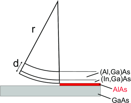
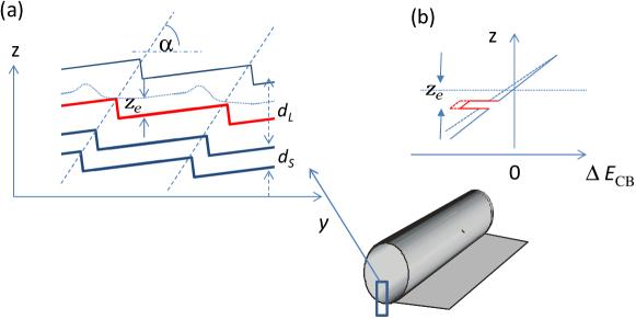
The self-rolling of thin pseudomorphically strained semiconductor bilayer systems based on epitaxial heterojunctions grown by molecular-beam epitaxy (MBE) was proposed by Prinz et al.Prinz et al. (2000) Such structures allow for investigation of the physical properties of systems with nontrivial topology. A new research field was opened: It became possible to create a high-mobility two-dimensional electron gas (HM2DEG) on cylindrical surfaces. In these structures, the low-temperature mean free path of the electrons can be kept comparable to the curvature radius .Friedland et al. (2007); Vorobev et al. (2007) In this case, the modifications of the adiabatic motion of electrons on cylindrical surfaces lead to trochoid- or snake-like trajectories Friedland et al. (2007) or additional structures in the quantum Hall effect.Friedland et al. (2009) The local structure of rolled-up single crystalline structures was already investigated in detail by x-ray micro-diffraction.Krause et al. (2006); Malachias et al. (2009) A review about the structure of radial superlattices is given in Ref.(Deneke et al., 2009). Here we demonstrate that lateral strain fluctuation arising during the stress relaxation by the release from the substrate and the self-rolling of the strained semiconductor bilayer systems significantly affects the adiabatic motion of the electrons on curved surfaces. Figure 1 illustrates the self-rolling of an (Al,Ga)As/GaAs quantum well (QW) structure and an (In,Ga)As stressor film after etching away a sacrificial AlAs film underneath the (In,Ga)As film. The originally tetragonally strained (In,Ga)As film can now expand laterally (parallel to the hetero-epitaxial interface) by curving the whole remaining stack, i.e. the thin (Al,Ga)As/GaAs QW structure grown epitaxially on top of the stressor film, like a bimetal strip. is the thickness of the layer stack. The radius of the cylindrical structure is determined by the thicknesses and elastic moduli of its individual layers.Grundmann (2003) Simultaneously, the self-rolling process itself creates a new strain topology in the layers. First, a gradient exists ranging from compressive to tensile strain in a rolled-up layer stack normal to the layer surface. The difference between the strain at the upper and lower surfaces of the stack is . Furthermore, a lateral fluctuation of the local strain is caused by tiny variations of the layer stack thicknesses , which arise on different length scales. On a lateral length scale of several micrometers, thickness fluctuation occurs due to step bunching during the MBE growth procedure with peak-to-peak height differences of 1–2 nm.Kondrashkina et al. (1997); Jenichen et al. (1997) Consequently, for a low value of , this leads to an essentially inhomogeneous strain field penetrating the structures. The thickness fluctuation has a large influence on the electronic properties of self-rolling systems, which lack the stabilizing influence of a thick substrate. This thickness fluctuation and the corresponding strain inhomogeneities cause lateral changes of the energy gap of the structures leading to variations of the quantum well confinement energies.Jahn et al. (1994, 1995, 1996) Consequently, for the respective cylindrical structures with a radius of m, we should expect an overall strain fluctuation of , which translates into energy fluctuation up to meV (deformation potential eV Yu and Cardona (1995)). In the present work, we show that layer thickness fluctuation on a nanometer scale leads to a phase cancelation of the Shubnikov-de-Haas (SdH) oscillations in the curved HM2DEG.
II Experiment
Strained, multilayered films (SMLF) with overall thicknesses of 150–170 nm were grown by MBE on top of a nominally =24 nm thick (In,Ga)As stressor layer. Each of the SMLF included a HM2DEG in a remotely doped GaAs quantum well (QW) structure. The barriers of the QW consisted of AlAs/GaAs short-period superlattices (SL) with Si- doping in one of the GaAs sequences in the SLs on both sides of the QW. This specific structure allows for a high electron mobility even in freestanding layers.Friedland et al. (1996, 2001) The surface morphology of the flat samples was studied by atomic force microscopy (AFM) in ambient air using a Digital Instrument Nanoscope. High-resolution x-ray diffraction (XRD) measurements were performed on the flat as-grown structures using a Panalytical X-Pert PRO MRD™ system with a Ge(220) hybrid monochromator (Cu K radiation with a wavelength of Å). The program Epitaxy™ was used for data evaluation. is the angle between the incident x-ray beam and the sample surface. 2 is the detector angle with respect to the incident beam.
The depth profile of the displacement of the original layer stack was calculated directly by the phase retrieval method Nikulin (1998); Nikulin and Zaumseil (1999) from synchrotron x-ray diffraction data. The synchrotron experiment was conducted on BL13XU at SPring-8. An x-ray energy of 12.4 keV was selected by the primary Si(111) channel-cut beamline monochromator. Further collimation and monochromatization of the beam were performed using a secondary channel-cut Si(400) monochromator. We recorded diffracted intensity profiles as a function of the sample angle and location of the incident beam on the sample surface. The experimental parameters allowed us to achieve a spatial resolution in the resulting strain depth profiles of 0.5 nm. Plane wave illumination was performed using a 20 m wide slit in the direction of the diameter of the roll. The other dimension of the beam (perpendicular to the diffraction plane) was 100 m. The location of the incident beam on the sample surface was changed with a linear step of 5 m.
For the investigation of curved HM2DEG’s, we first fabricated conventional Hall bar structures in the planar heterojunction along the crystal direction with three 4 m wide lead pairs, separated by 10 m in a similar manner as used in Ref. Friedland et al., 2009. Then, the SMLF including the Hall bar was released by selective etching of the sacrificial AlAs layer with a 5 HF acid/water solution at 4 ∘C starting from a edge. In order to relax the strain, the SMLF rolled up along the direction forming a complete tube with a radius of about 20 m. The direction of the current in the Hall bar was along the circumference of the tube. For our measurements of the SdH oscillations in the longitudinal resistances, we thoroughly aligned the direction of the magnetic field perpendicular to the cylinder surface at the position in the middle between the terminals for the resistivity measurements by minimizing the asymmetry effects in the magnetotransport data, caused by the magnetic field gradient .Friedland et al. (2009) All resistance measurements were carried out at temperature = 50 mK. We determined a mobility mVs-1 and a carrier density of m-2.
Spatially resolved measurements of the luminescence of the cylindrical structures were performed by cathodoluminescence spectroscopy (CL) in a scanning electron microscope (SEM). Secondary electron (SE) and monochromatic CL images were acquired simultaneously for an accurate assignment of the local origin of the CL. The CL/SE experiments were performed using a Zeiss ULTRA55 field emission SEM equipped with the Gatan monoCL3 and a He-cooling stage system. The acceleration voltage was 5 kV while the beam current was 5 nA at a sample temperature of 7 K. The spectral resolution amounted to 0.3 nm corresponding to a slit width of the CL spectrometer of 0.1 mm.
We investigated always samples from the same MBE growth run by all the different methods. In our experience the inhomogeneity of the MBE grown wafer in terms of composition and layer thickness is below 5%. An error of 5% can be tolerated for the considerations in the present work. From the MBE grown samples many rolls were prepared and some of them were investigated by SEM, others by transport measurements. We assume, that the roughness of the interfaces arises during the MBE growth procedure and is not changed by the rolling. From XRD and AFM we obtain quantitative data of the root mean square (RMS) roughness according to standard procedures. In addition we obtain from AFM quantitative data of the peak-to-peak height values in typical AFM micrographs. All this data is obtained from as-grown samples. The AFM and x-ray data are representative for the step flow growth mode of MBE [see Ref.(Kondrashkina et al., 1997; Jenichen et al., 1997) and references therein].
III Results and Discussion
III.1 Surface and interface roughness
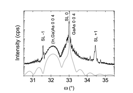
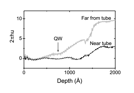
The RMS thickness fluctuation in multilayer structures can be detected by XRD via a broadening of their SL maxima.Speriosu and Vreeland (1984); Holy et al. (1992); Proctor et al. (1994); Pan et al. (1999) Figure 2 displays an x-ray diffraction curve of the as-grown QW structure with AlAs/GaAs SL barriers near the GaAs 004 reflection. The simulation below was performed for a 10 nm thick In0.19Ga0.81As stressor layer in order to illustrate the source of strain in the structure. The lattice parameter of the (In,Ga)As stressor layer is obviously larger than that of the (Al,Ga)As/GaAs QW structure. This is indicated by the smaller Bragg angle corresponding to the In0.19Ga0.81As film. From the positions of the satellite reflections of the AlAs/GaAs barrier SL, we obtained an average SL period of = 3.64 nm. Figure 3 shows displacement profiles inside the layer stack obtained by the x-ray phase retrieval method.Nikulin (1998); Nikulin and Zaumseil (1999) denotes the displacement and the magnitude of the reciprocal lattice vector of the corresponding reflection (004). The position of the GaAs QW is marked by an arrow. These profiles were calculated from measurements using a highly intense and highly collimated micro-beam of synchrotron radiation as an incident beam. In this way, a lateral resolution of about 5.0 m was achieved during the x-ray diffraction experiment. Far away from the micro-tube, the displacement profile as expected from the nominal structure of the layer stack was obtained. Even the individual periods of the short period SLs can be observed. In the vicinity of the micro-tube we detected stress relaxation near the QW and the barrier layers (Fig. 3). The tube itself could not be measured even in the synchrotron experiment. The very high collimation of the synchrotron beam (quasi-plane wave) leads to rather narrow regions where diffraction conditions are fulfilled in a structure with as small radius of curvature as 20 m. This results in a severe reduction of the diffracted signal.
The presence of AlAs/GaAs SL barriers in the QW structures opens up the possibility of a direct measurement of the thickness fluctuation inside the layer stack. Note that, before the QW structure with its AlAs/GaAs SL barriers was fabricated, a thick GaAs buffer layer was grown in order to start the growth of the QW structures with a clean surface without substrate defects. During this buffer layer growth, the substrate roughness was not simply repeated, but a certain modification by step bunching can be expected, especially during MBE growth in the step-flow mode. We now characterize the two different kinds of roughness arising in our structures. First we look at the RMS roughness. Neglecting absorption, the diffracted intensity of a SL with periods can be written as Speriosu and Vreeland (1984)
| (1) |
where
| (2) |
denotes the SL period, the Bragg angle of the substrate, and the grazing angle of incidence with respect to the diffracting planes, which we assume to be parallel to the surface. is the direction cosine of the diffracted wave, the x-ray wavelength, and the strain normal to the surface. is the structure factor of the SL and is a slowly varying function of . Let with being the peak order. Around , i.e. near a satellite position, Eq. (1) can be approximated by a smoothed function Zachariasen (1994); Pan et al. (1999)
| (3) |
The full width at half maximum (FWHM) of such a smoothed peak of an ideal SL can be written as Zachariasen (1994); Pan et al. (1999)
| (4) |
where denotes the angular spacing between neighboring satellite peaks
| (5) |
Let us now describe the period of the real SL as . The fluctuation of can be described by a Gaussian distribution function with standard deviation , where is the center value of the distribution function and is the deviation from . Then, the diffracted intensity becomes
| (6) |
In this approximation, we can describe the broadening of the -th satellite peak as Pan et al. (1999)
| (7) |
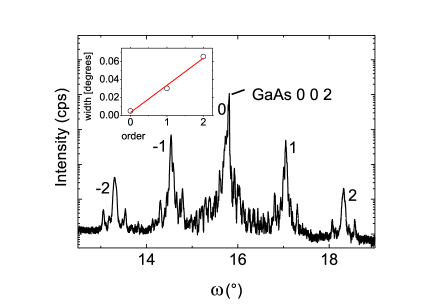
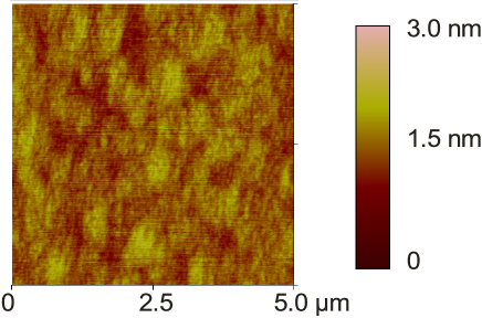
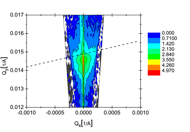
Here, the first term represents an intrinsic width of the satellite peaks, and the second term is a result of the periodicity fluctuation . From the experimentally determined peak-widths , the magnitude of the periodicity fluctuation can be obtained. Figure 4 displays an XRD curve near the quasi-forbidden GaAs 002 reflection. The satellite maxima of the AlAs/GaAs SLs forming the barriers of the QW are marked by their order. Higher-order satellites are clearly broadened compared to the zeroth order. An evaluation of the broadening of the satellite maxima using Eq. (7) yields a fluctuation value of = 0.1 nm , which is a measure for the RMS roughness. Similar values for the surface and interface RMS roughness were determined by x-ray reflectivity measurements (not shown here). Figure 5 shows an AFM micrograph of the surface of the same sample. The values of the RMS interface roughness of = 0.1 nm determined by XRD and the RMS surface roughness of about 0.2 nm as determined by AFM are in good agreement. Besides the extraordinary low RMS roughness of about 0.2 nm, there are surface inhomogeneities on the larger lateral length scale. Their amplitude amounts to 2 nm. A clear azimuthal asymmetry of the island shape is observed. However, the AFM investigations showed that besides the small-scale average roughness there are other inhomogeneities of the surface on a larger lateral lengthscale of 1.0 m. They are caused by the step-bunching during MBE growth resulting in a clear azimuthal anisotropy of the surface roughness. Such large-scale inhomogeneities are typical for MBE growth in the step-flow growth mode and have already been reported in Refs. Kondrashkina et al., 1997; Jenichen et al., 1997. In addition to the differences between several growth modes, the skew inheritance of the interface roughness during epitaxial growth of semiconductor superlattices was revealed. Figure 6 demonstrates the intensity distribution of the diffuse x-ray scattering under grazing incidence in order to check the inheritance angles for our sample. Along GaAs[110], we found an inheritance angle 60∘, while along the perpendicular direction [10] it was = 83∘. As a result, we really found a skew inheritance leading to layer thickness inhomogeneities on the larger lateral length scale. The step bunching leads to thickness inhomogeneities in the short period SLs, the QW, and the (In,Ga)As stressor layer.
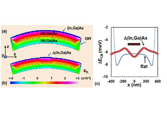
We will now estimate the effect of the thickness inhomogeneities of the (In,Ga)As stressor layer on the local strain and the electronic energy of the structure. Calculations of the strain distribution in the tubes were carried out by the finite-element method Elmer (2012). Exact strain calculations for tubes with varying layer thicknesses require complex and time-consuming three-dimensional calculation models. In order to simplify the numerical procedure, calculations were performed in two steps. In the first step, we analytically determined the strain field in a layer stack with a flat (In,Ga)As layer by assuming that it remains flat after detachment from the substrate. The thicknesses and elastic constants of the layers in the stack as well as the in-plane strain due to the lattice mismatch () relative to the GaAs substrate are given in Tab. 1. The strain calculated in this way was used as the driving force for the rolling process. The stack was allowed to roll along one direction (-direction): the evolution of the strain during the rolling process was determined by a two-dimensional finite element approach.
Figure 7(a) displays the distribution of the hydrostatic strain calculated for a structure with a flat (In,Ga)As stressor (13 nm thick). The strain variation close to the left and right ends of the roll are due to relaxation. In contrast, the strain in the center region is approximately constant in the QW plane. Note that due to the bending the hydrostatic strain changes from tensile in the upper (Al,Ga)As layer to compressive in the lower one, the plane of zero strain strain (i.e., ) being located above the GaAs QW. Figure 7(b) shows the results of similar calculations for a structure with a 11 nm thick (In,Ga)As layer containing a 200 nm long region [indicated by (In,Ga)As] with a larger thickness of 15 nm. The additional tensile strain induced by this region extends to a depth comparable to its width, thereby modifying the strain distribution in the QW. Figure 7(c) displays profiles for the variation of the conduction band (CB) energy (relative to the CB energy of unstrained GaAs) along the QW plane calculated assuming a CB deformation potential eV Yu and Cardona (1995). A careful examination of the strain profile along the QW plane in Fig. 7(c) shows that is larger below the (In,Ga)As region. As for the strain distribution in Figs. 7(a) and 7(b), the variations at the ends of the roll are due to strain relaxation. For the roll with an (In,Ga)As layer of constant thickness, is approximately constant in the central region of the roll. For the roll in Fig. 7(b), the increased thickness of the (In,Ga)As layer induces an increase in the tensile strain close to the center of the roll, which increases by approximately 1.6 meV.
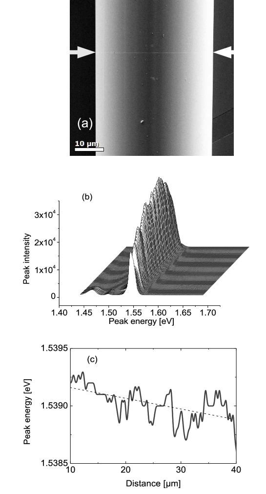
A highly sensitive method for the characterization of QW structures with high lateral resolution is CL spectroscopy performed in an SEM. We applied CL spectroscopy for the characterization of the curved QWs, prepared from those samples, which were already investigated by XRD and AFM. The electron beam was scanned across a typical micro-tube containing the GaAs QW. A line scan is depicted in in Fig. 8(a). The corresponding energy spectra are given in Fig. 8(b). The CL intensity distribution (not shown here) is very similar to the AFM surface topography pattern in Fig. 5. This proves that the inhomogeneities of the CL energy are caused by the thickness fluctuation of the GaAs QW in the micro-tube and/or strain fluctuation due to the thickness fluctuation in the AlAs/GaAs SL barriers. The corresponding spatial distribution of the energy detected during the CL line scan is shown in Fig. 8 (c). This energy variation directly reflects the variation of the bandgap and at the same time the variation of the chemical potential. The CL line is due to the bandgap luminescence for the given QW with especially high electron density. The fluctuation of the peak energy of the CL line reflects the fluctuation of the chemical potential of the QW on a micrometer-scale and amounts to 0.2 meV.
Now we can develop a simple model for the estimation of density fluctuation in the given cylindrical structures caused by thickness fluctuation resulting from the step bunching due to an inclined step height inheritance during the MBE growth (cf. Fig. 9). Note that the QW as a part of the layer stack has a similar roughness as the structure below, which is however shifted laterally due to the finite inclination (inheritance) angle . By releasing and rolling up the layer stack containing the QW (cf. Fig. 1), the strain along the -direction normal to the layer arises and fluctuates along the cylinder surface, indicated as the -direction per definition in Fig. 9, due to variations of the thicknesses and . Consequently, the CB energy shifts according to the actual value of . For our particular (In,Ga)As/(Al,Ga)As layer stack, we calculated the energy shift in accordance with the model described in Ref. Hey et al., 2009. The results of these calculations are shown in Fig. 9(b) for two different thicknesses of the (In,Ga)As stressor layer. The lower part of the layer stack, which contains the (In,Ga)As stressor layer and also the QW, is under tensile strain. The upper part of the stack is under compressive strain. The position of zero strain and thereby zero-energy shift is marked in Fig. 9(a) by a dotted line derived from and . Taking this into account, we assume that the distance between the zero-strain line and the position of the 2DEG fluctuates with an amplitude which is similar to the layer thickness fluctuation 1 nm. As a result, we estimate the fluctuation of the conduction band energy as meV, where kV/m denotes the strain induced electrical field. This value is in good correspondence to the energy fluctuation observed in the CL measurement.
III.2 Phase cancelation of the SdH oscillations
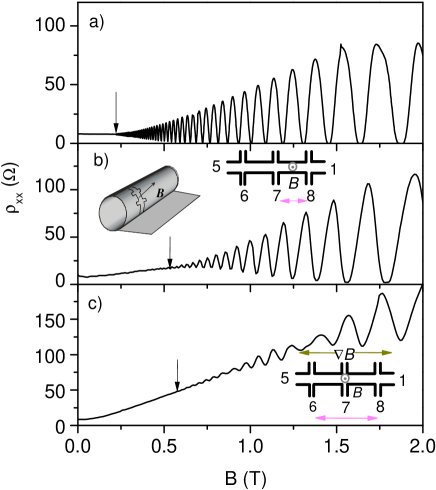
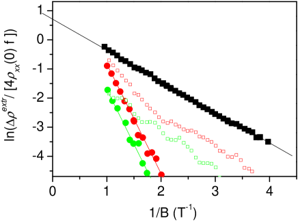
Figure 10 compares the longitudinal resistivities as a function of the magnetic field in the region of the SdH oscillations for Hall bar structures on flat (a) and cylindrical surfaces (b) and (c). The terminals for the measurement of are separated by m and m for the traces in Figs. 10 (b) and (c), respectively. In Tab. LABEL:table1 the results of the cancelation of the SdH oscillations are collected. Note that the low-field mobilities and carrier densities do not differ significantly in both samples. This shows that the self-rolling process does not introduce additional defects and surface depletion of the HM2DEG density. However, the magnitude of the SdH oscillations is strongly reduced in the cylindrical structures. Moreover, visible SdH oscillations appear at much higher magnetic field values of about = 0.5 – 0.6 T for the cylindrical surface as compared to 0.2 T for the flat surface. The so-called ’Dingle plot’ is used to characterize the magnetic field dependence of the magnitude of the SdH oscillations in .Coleridge (1991) It allows for an estimation of the total scattering time from , which is the difference between the zero-field resistance and at the resistance oscillation extremes in accordance with the conventional Ando formula
| (8) |
where with ) accounts for thermal smearing. denotes the cyclotron frequency and the effective electron mass.Mancoff et al. (1996) Fig. 11 demonstrates the Dingle-plots for the flat sample (a) and for the curved samples (b) and (c). These graphs present the function ln(]) plotted versus . For the flat sample, the experimental points follow precisely the Ando formula. They can be approximated by a straight line, which intersects the axis = 0 at the ordinate value of . We can estimate a total scattering time = 1.12 ps, which is mostly governed by small-angle scattering processes, in contrast to the much larger transport scattering time = 50 ps, which is determined by large-angle scattering events (cf. Tab. LABEL:table1).
The strong reduction of the SdH oscillations in curved samples increases the slope of the corresponding lines in this representation, which leads to nearly three times lower values of as compared to the flat one (cf. Tab. LABEL:table1). In addition, the extrapolation of the linear fit does not intersect the = 0 axis at the ordinate value of . Such a behavior was earlier discussed in the context of sample inhomogeneities.Coleridge (1991) An obvious reason for sample inhomogeneities is the curvature of the Hall bar resulting in a magnetic field gradient, which surely leads to a smearing of the SdH oscillation.
In order to prove, if the smearing effect due to the magnetic field gradient can explain the low values of , we present in Fig. 11 also the results of averaging the data of the flat sample [cf. Fig. 10(a)]. We calculate the average value cos(]. Here, sin()=, m, = 0,1,2,.. up to , for the terminal distances m and m according to the measurements [cf. Figs. 10(b) and 10(c)]. The corresponding Dingle-plots show oscillations, which arise from the beating of two modes, belonging to the minimum and maximum values of the magnetic field in the Hall bar. Such a beating was already observed in the SdH oscillations at much larger gradients of the field.Friedland et al. (2009) In fact, this averaging by curvature reduces the magnitude of the SdH oscillations effectively, but it does not change the slope of the Dingle plot. Moreover, this effect does not eliminate the large extrapolation values at = 0. It seems that the experimental data can be approximated by a straight line corresponding to the averaging by means of the magnetic field gradient at higher magnetic fields. Unfortunately, all the data at magnetic fields above 1 T show a clear signature of the quantum Hall effect, which results in a completely different dependence of on the magnetic field.Friedland et al. (2009)
Another source of lateral inhomogeneities may be the so-called ’static skin’ effect.Chaplik and Chaplik (2000); Friedland et al. (2010) The gradient of the field results in a redistribution of the current flow toward one of the edges of the Hall bar, which changes the side by reversing the magnetic field direction. For the present geometry, the skin length , which determines the width of the conducting channel, is below 1 m at the position with the maximal field gradient T. is twice as large in the measurement shown in Fig. 10(c) compared to measurement shown in Fig. 10(b). However, both samples behave nearly identically in the Dingle plots, so that we have to reject the static skin effect as a cause for the reduced SdH oscillations in the curved samples.
Finally, we discuss the consequences of strain fluctuation. In a cylindrical structure with a HM2DEG, the resulting energy fluctuation is a fluctuation of the conduction band energy. Therefore, the chemical potential and the carrier density of the HM2DEG vary in accordance with the strain fluctuation. The impact of density fluctuation on the magnitude of the SdH oscillations was already identified as a phase cancelation, which reduces the magnitude of the SdH oscillation due to a broadening of the Landau level width. The corresponding change in density necessary for the phase cancelation of the SdH oscillations is given in Ref. Harrang et al., 1985 as
| (9) |
With the observed onset 0.56 T of the SdH oscillations in the cylindrical structures, we estimate m-2. This value may be used to calculate
the fluctuation meV and
of the chemical potential and the relative Fermi wave vector, respectively. The
latter introduces a scattering angle of about one degree, which proves that the observed phase cancelation is a low-angle
scattering effect. We estimate the quantum relaxation time due to density
fluctuation 1.4 ps. Then, the
value 0.64 ps is in a good
agreement with the measured low-angle scattering time in the cylindrical
structures (cf. Tab. LABEL:table1). The value of is in good agreement with obtained from the energy
fluctuation of the QW obtained by CL spectroscopy.
We can estimate the density
fluctuation as m-2 from the fluctuation of the conduction band energy ,
which is in a good agreement with the value estimated from the damping of the SdH oscillations.
IV Conclusion
The strain state in released (In,Ga)As/(Al,Ga)As micro-tubes was characterized by strain fluctuation with a lateral correlation length of about 1.0 m. This strain fluctuation images the thickness inhomogeneities, which are due to step bunching during epitaxial growth of the original layer. They lead to a local variation of the chemical potential and, therefore, to fluctuation of the carrier density. This results in a phase cancelation of the Shubnikov-de-Haas oscillations in the curved HM2DEG and, therefore, in a degradation of the single-electron scattering time, whereas the electron mobility in these structures remains high. The estimated fluctuation of the carrier density agrees well with the energy fluctuation measured in cathodoluminescence spectra of the free-electron transition of the quantum well.
V Acknowledgement
The authors thank A. Riedel and M. Höricke for sample preparation, H. T. Grahn and J. Herfort for a critical reading of the manuscript, and V. M. Kaganer for helpful discussions. We acknowledge the help of O. Sakata of on BL13XU during the experiment performed at SPring 8.
VI References
References
- Prinz et al. (2000) V. Y. Prinz, V. A. Seleznev, A. K. Gutakovsky, A. V. Chehovskiy, V. V. Preobrazhenskii, M. A. Putyato, and T. A. Gavrilova, Physica E (Amsterdam) 6, 828 (2000).
- Friedland et al. (2007) K. J. Friedland, R. Hey, H. Kostial, A. Riedel, and K. H. Ploog, Phys. Rev. B 75, 045347 (2007).
- Vorobev et al. (2007) A. B. Vorobev, K. J. Friedland, H. Kostial, R. Hey, U. Jahn, E. Wiebicke, J. S. Yukecheva, and V. Y. Prinz, Phys. Rev. B 75, 205309 (2007).
- Friedland et al. (2009) K. J. Friedland, A. Siddiki, R. Hey, H. Kostial, A. Riedel, and D. K. Maude, Phys. Rev. B 79, 125320 (2009).
- Krause et al. (2006) B. Krause, C. Mocuta, T. H. Metzger, C. Deneke, and O. G. Schmidt, Phys. Rev. Lett. 96, 165502 (2006).
- Malachias et al. (2009) A. Malachias, C. Deneke, B. Krause, C. Mocuta, S. Kiravittaya, T. H. Metzger, and O. G. Schmidt, Phys. Rev.B 79, 035301 (2009).
- Deneke et al. (2009) C. Deneke, R. Songmuang, N. Y. Jin-Phillip, and O. G. Schmidt, J. Phys. D: Appl. Phys. 42, 103001 (2009).
- Grundmann (2003) M. Grundmann, Appl. Phys. Lett. 83, 2444 (2003).
- Kondrashkina et al. (1997) E. A. Kondrashkina, S. A. Stepanov, R. Opitz, M. Schmidbauer, R. Köhler, R. Hey, M. Wassermeier, and D. V. Novikov, Phys. Rev. B 56, 10469 (1997).
- Jenichen et al. (1997) B. Jenichen, R. Hey, M. Wassermeier, and K. Ploog, Il Nuovo Cimento D 19, 429 (1997).
- Jahn et al. (1994) U. Jahn, K. Fujiwara, J. Menniger, R. Hey, and H. T. Grahn, J. Appl. Phys. 77, 1211 (1994).
- Jahn et al. (1995) U. Jahn, K. Fujiwara, R. Hey, J. Kastrup, H. T. Grahn, and J. Menniger, J. Cryst. Growth 150, 43 (1995).
- Jahn et al. (1996) U. Jahn, J. Menniger, R. Hey, B. Jenichen, E. Runge, and H. T. Grahn, Mater. Sci. Eng. B 42, 133 (1996).
- Yu and Cardona (1995) P. Yu and M. Cardona, Fundamentals of Semiconductors (Springer, Heidelberg, 1995).
- Friedland et al. (1996) K. J. Friedland, R. Hey, H. Kostial, R. Klann, and K. Ploog, Phys. Rev. Lett. 77, 4616 (1996).
- Friedland et al. (2001) K. J. Friedland, A. Riedel, H. Kostial, M. Höricke, R. Hey, and K. H. Ploog, J. Electron. Mater. 90, 817 (2001).
- Nikulin (1998) A. Y. Nikulin, Phys. Rev. B 57, 11178 (1998).
- Nikulin and Zaumseil (1999) A. Y. Nikulin and P. Zaumseil, Phys. Status Solidi A 172, 291 (1999).
- Speriosu and Vreeland (1984) V. S. Speriosu and T. Vreeland, J. Appl. Phys. 56, 1591 (1984).
- Holy et al. (1992) V. Holy, J. Kubena, I. Ohlidal, and K. H. Ploog, Superlatt. Microstr. 12, 25 (1992).
- Proctor et al. (1994) M. Proctor, G. Oelgart, H. Rhan, and F. K. Reinhart, Appl. Phys. Lett. 64, 3154 (1994).
- Pan et al. (1999) Z. Pan, Y. T. Wang, Y. Zhuang, Y. W. Lin, Z. Q. Zhou, L. H. Li, R. H. Wu, and Q. M. Wang, Appl. Phys. Lett. 75, 223 (1999).
- Zachariasen (1994) W. H. Zachariasen, Theory of X-ray Diffraction in Crystals (Dover Publications Inc., New York, 1994).
- Elmer (2012) Elmer, Open Source Finite Element Software for Multiphysical Problems (http://www.csc.fi/english/pages/elmer, Espoo, 2012).
- Hey et al. (2009) R. Hey, M. Ramsteiner, P. Santos, and K. J. Friedland, J. Cryst. Growth 311, 1680 (2009).
- Coleridge (1991) P. T. Coleridge, Phys. Rev. B 44, 3793 (1991).
- Mancoff et al. (1996) F. B. Mancoff, L. J. Zielinski, C. M. Marcus, K. Campman, and A. C. Gossard, Phys. Rev. B 53, 7599 (1996).
- Chaplik and Chaplik (2000) A. Chaplik and V. Chaplik, JETP Lett. 72, 503 (2000).
- Friedland et al. (2010) K. J. Friedland, R. Hey, A. Riedel, and D. K. Maude, Phys. Status Solidi C 7, 2562 (2010).
- Harrang et al. (1985) J. P. Harrang, R. J. Higgins, R. K. Goodall, P. R. Jay, M. Laviron, and P. Delescluse, Phys. Rev. B 32, 8126 (1985).
| thickness | epi-strain | |||
|---|---|---|---|---|
| (nm) | (N/m2) | (N/m2) | ||
| In0.24Ga0.76As | 15 | 1.6810-2 | 1.101011 | 5.131010 |
| Al0.33Ga0.67As | 62 | 4.5810-4 | 1.191011 | 5.451010 |
| GaAs QW | 13 | 0 | 1.181011 | 5.321010 |
| Al0.33Ga0.67As | 62 | 4.5810-4 | 1.191011 | 5.451010 |
| Hall bar | density | mobility | |||
|---|---|---|---|---|---|
| m | (m) | sec) | sec) | (T) | |
| flat | 6.32 | 126 | 50 | 1.15 | 0.19 |
| flat-average m | 6.32 | 126 | 50 | 0.19 | |
| curved m | 6.28 | 118 | 46 | 0.43 | 0.56 |
| curved m | 6.28 | 118 | 46 | 0.43 | 0.57 |