Magnification effects in scanning tunneling microscopy: the role of surface radicals
Abstract
Scanning tunneling microscopy (STM) is a fundamental tool for determination of the surface atomic structure. However, the interpretation of high resolution microscopy images is not straightforward. In this paper we provide a physical insight on how STM images can suggest atomic locations which are distinctively different from the real ones. This effect should be taken into account when interpreting high-resolution STM images obtained on surfaces with directional bonds. It is shown that spurious images are formed in the presence of polarized surface radicals showing a pronounced angle with respect to the surface normal. This issue has been overlooked within the surface science community and often disregarded by experimentalists working with STM. Without loss of generality, we illustrate this effect by the magnification observed for pentamer-like structures on , and surfaces of silicon and germanium.
![[Uncaptioned image]](/html/1907.08919/assets/x1.png)
TOC Graphical entry
University of Aveiro]Department of Physics & I3N, University of Aveiro, Campus Santiago, 3810-193 Aveiro, Portugal \alsoaffiliation[Institute of Semiconductor Physics]Institute of Semiconductor Physics, pr. Lavrentyeva 13, Novosibirsk 630090, Russia University of Aveiro]Department of Physics & I3N, University of Aveiro, Campus Santiago, 3810-193 Aveiro, Portugal \phone+351 234 247051 \fax+351 234 378197 The study of the atomic structure of a crystal surface often starts with scanning tunneling microscopy (STM) measurements. The positions of bright spots in high resolution STM images are then associated with exact atomic coordinates on the surface under scrutiny. Although being generally accepted, such a connection is known to be imperfect with several deceiving cases being known. The STM images obtained from Bi-terminated Si and Ge surfaces are clear examples1, 2 — while bright spots are observed atop of the Bi trimers at negative bias and at large positive bias, at low positive bias the spots are observed between trimers, where no atoms exist.
It is clear that the interpretation of high-resolution STM images is not straightforward. According to a simplified view, STM images obtained in a constant-current mode represent a combination of surface topography and local density of electronic states.3, 4 Consequently, a full reasoning of such images, may only be possible upon some knowledge of the surface atomic structure (which is often unavailable), or with the assistance by ab-initio electronic structure calculations.
While the connection between the surface atomic positions and bright spots in STM images is often factual and correct (and so it may be the resulting model), we show below that surface geometry misassignments are likely to occur when the electronic polarization and hybridization of states at surface atoms are overlooked. We illustrate the occurrence of large offsets between bright spots from STM images and the corresponding atomic nuclei with help of a paradigmatic example, namely with the magnification of pentamers as seen in STM images of Si.5 Analogous pentameric structures were found on and surfaces of silicon and the surface of germanium.6, 7, 8

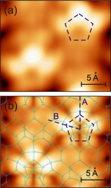
Figure 1(a) depicts an experimental high-resolution STM image at positive bias ( V) of the Si surface showing bright pentameric features.5 The bright spots at the corners of one of the pentamers are connected by dashed lines. The distance between two nearest spots is about as derived from the experimental STM image in Fig. 1(a).
Figure 1(b) shows the 8P atomic model for the Si reconstruction,5 along with its respective STM image obtained from the calculated LDOS at positive bias (considering states up to eV above the Fermi level) within the Tersoff-Hamann approximation.3 The image in Fig. 1(b) represents the height at constant integrated LDOS between +0.8V and Fermi level for Si. It gives an idea of how an STM image of the Si surface would look like for an infinitesimally sharp tip, i.e. close to a single atom with an s-orbital. The distance between the nearest bright spots within the pentamers of Fig. 1(b) agrees well the analogous distance as derived from the experimental STM image of Fig. 1(a). However, the overlaid atomic structure shown in Fig. 1(b) clearly shows that the actual distance between nearest Si atoms in each pentamer is , corresponding to an experimental deviation of more than 50% with respect to atomic positions. Due to its magnitude, this mismatch sustained an argument against atomic models of and silicon surfaces involving five-fold rings of Si atoms.9, 10, 11

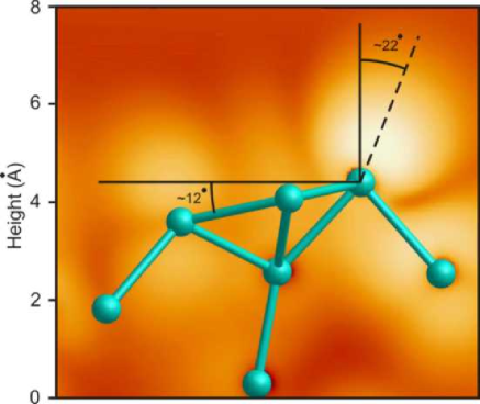
Figure 2 shows a vertical cut of the height at constant integrated LDOS (between +0.8V and Fermi level) across the ‘A’ dashed line of Fig. 1(b) ( crystallographic direction) combined with a projection of a pentamer atomic structure. The brightest spot at the upper right corner of Fig. 2 shows a high intensity for the empty LDOS located near the Si radical at the upmost apex of the pentamer in Fig. 1(b). Clearly, the radical state does not point upwards (along ), rather making an angle of about 22∘ with respect to surface normal and away from the center of the pentamer. Since STM is intrinsically sensitive to LDOS,3 and becasue the tip usually hoovers between 4 to 10 Å above the surface,4 it becomes evident that the slanted radicals will project a magnified image of the underlying pentamer. This explains the apparent contradiction between the size of the pentamers from the atomistic model and those derived directly from STM images (see Refs. 9 and 10).
The distortion of the pentamers as observed by STM should not be confused with another spurious effect which arises from the finite size of the STM tip. The measured surface topography can be represented as a convolution of the real surface topography and the shape of STM tip.12 This effect leads to broadening of the objects protruded out of the surface for the case of a dull tip. Comparing experimental and calculated STM images in Fig. 1, we realize that the image in Fig. 1(a) is indeed affected by the latter effect – the experimental image is more diffuse than the calculated one. The contribution of the finite tip size effect to the magnification of the pentamers must be however minor. A 50% increase of the pentamer size (as observed in Fig. 1(b)) would imply a severe and inhomogeneous broadening of the bright spots, which would not fit the experimental data.

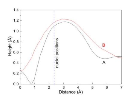
Figure 3 shows the height profiles measured across the bright spots in the calculated STM image of Fig. 1(b). The horizontal axis runs from the center of a pentamer either along ‘A’ or ‘B’ dashed lines. The vertical dashed line in Fig. 3 represents the actual position of the Si nuclei in the pentamer, clearly showing that they do not coincide with positions of the maxima. The lateral bright spot along ‘B’ is more diffuse then the spot close to the central apex along ‘A’. This feature is also observed on the experimental STM images, and that is due to the inclination of a pentamer plane with respect to the surface normal by about 22∘ towards the direction (see Fig. 2).
The observation of spurious images by STM as described above is not limited to the case of pentamers in the , , surfaces of silicon and germanium. It should be observed virtually on any surface having directional dangling bonds whose axes are not normal to the surface. Of course this will essentially depend on the specific surface bonding and reconstruction details, which can be scrutinized by first-principles atomistic methods.
Establishing a direct connection between the positions of bright spots in STM images and the positions of atomic nuclei can lead to considerable sizing and interpretation errors. For example, the Si surface orientation composed of regularly spaced terraces and triple steps has been erroneously identified. While an early STM study on this subject indicated a orientation [9.5∘ off the plane],13 latter works including high resolution diffraction data report a orientation [10.0∘ off the plane].14, 15, 16, 17, 18, 19
In conclusion, we demonstrated that the positions of bright spots in high resolution STM images and the actual coordinates of atomic nuclei may differ substantially. Elusive images can be formed on surfaces having dangling-bond states whose main axis differs from the surface normal, and that may lead to misinterpretation of the experimental data. Pentameric structures on Si(331) observed by STM provided a showcase for the above effect, which if taken into account, reconciles the conflicting theoretical and measured sizes of pentamers occurring on , and surfaces of Si and Ge.
Experimental and computational methods
The measurements were performed in an ultrahigh vacuum chamber () on a system equipped with an Omicron STM. A clean Si(331) surface was prepared by sample flash annealing at 1250∘C for 1 min followed by stepwise cooling with 2∘C per minute steps within a temperature range 400-850 . The STM images were recorded at room temperature in the constant-current mode using an electrochemically etched tungsten tip.
Electronic structure calculations were carried using the density-functional plane-wave code.20, 21, 22, 23 The many-body exchange-correlation interactions were accounted for within the semi-local generalized gradient approximation.24 Core electrons were replaced by efficient projector-augmented wave (PAW) potentials,25, 26 allowing a description of the Kohn-Sham valence states using plane-waves with a cut-off energy of 250 eV.
The Si surface was represented by a periodic slab, consisting of ten atomic bilayers of silicon and of vacuum along the surface normal. The bottom side of the slab was passivated by hydrogen atoms, while the top side was prepared according to the 8P-model of the reconstruction as reported in Ref. 5. Atomic coordinates of the topmost eight bilayers were fully relaxed until the largest Hellmann-Feynman force became smaller than . The electron density (and potential terms) was obtained by sampling the band structure within the Brillouin zone using a -point grid.27 The local density of states (LDOS) for electrons at the surface was obtained from the Kohn-Sham eigenvalues and eigenfunctions. The STM images were calculated within the Tersoff-Hamann approach,3 assuming a constant current mode. The software was used to process the experimental and calculated STM images.28 {acknowledgement} The authors thank S. Teys for the given STM images. This work was funded by the Russian Foundation for Basic Research (Project No. 18-02-00025), the Fundação para a Ciência e a Tecnologia (FCT) under the contract UID/CTM/50025/2013, and by FEDER funds through the COMPETE 2020 Program.
References
- Mysliveček et al. 2010 Mysliveček, J.; Dvořák, F.; Stróżecka, A.; Voigtländer, B. Scanning tunneling microscopy contrast in lateral Ge-Si nanostructures on Si(111)--Bi. Physical Review B 2010, 81, 245427
- Zhachuk and Coutinho 2011 Zhachuk, R.; Coutinho, J. Ab initio study of height contrast in scanning tunneling microscopy of Ge/Si surface layers grown on Si(111) in presence of Bi. Physical Review B 2011, 84, 193405
- Tersoff and Hamann 1985 Tersoff, J.; Hamann, D. R. Theory of the scanning tunneling microscope. Physical Review B 1985, 31, 805
- Hofer 2003 Hofer, W. A. Challenges and errors: interpreting high resolution images in scanning tunneling microscopy. Progress in Surface Science 2003, 71, 147
- Zhachuk and Teys 2017 Zhachuk, R.; Teys, S. Pentagons in the Si(331)-() surface reconstruction. Physical Review B 2017, 95, 041412
- Dąbrowski et al. 1995 Dąbrowski, J.; Müssig, H.-J.; Wolff, G. A novel surface reconstruction: subsurface interstitials stabilize Si(113)-. Surface Science 1995, 331-333, 1022
- An et al. 2000 An, T.; Yoshimura, M.; Ono, I.; Ueda, K. Elemental structure in Si(110)-"" revealed by scanning tunneling microscopy. Physical Review B 2000, 61, 3006
- Stekolnikov et al. 2004 Stekolnikov, A. A.; Furthmüller, J.; Bechstedt, F. Structural elements on reconstructed Si and Ge(110) surfaces. Physical Review B 2004, 70, 045305
- Sakamoto et al. 2009 Sakamoto, K.; Setvin, M.; Mawatari, K.; Eriksson, P. E. J.; Miki, K.; Uhrberg, R. I. G. Electronic structure of the Si(110)-() surface: high-resolution ARPES and STM investigation. Physical Review B 2009, 79, 045304
- Teys 2017 Teys, S. A. Different STM images of the superstructure on a clean Si(133)- surface. JETP Letters 2017, 105, 477
- Zhachuk and Coutinho 2017 Zhachuk, R.; Coutinho, J. Comment on "Different STM images of the superstructure on a clean Si(133)- surface" (JETP Letters 105, 477 (2017)). JETP Letters 2017, 106, 346
- Schwarz et al. 1994 Schwarz, U. D.; Haefke, H.; Reimann, P.; Güntherodt, H.-J. Tip artefacts in scanning force microscopy. Journal of Microscopy 1994, 173, 183
- Kirakosian et al. 2001 Kirakosian, A.; Bennewitz, R.; Crain, J. N.; Fauster, T.; Lin, J.-L.; Petrovykh, D. Y.; Himpsel, F. J. Atomically accurate Si grating with 5.73 nm period. Applied Physics Letters 2001, 79, 1608
- Teys et al. 2006 Teys, S. A.; Romanyuk, K. N.; Zhachuk, R. A.; Olshanetsky, B. Z. Orientation and structure of triple step staircase on vicinal Si(111) surfaces. Surface Science 2006, 600, 4878
- Zhachuk and Pereira 2009 Zhachuk, R.; Pereira, S. Comment on "Atomic structure model of the reconstructed Si(557) surface with a triple step structure: adatom-parallel dimer model". Physical Review B 2009, 79, 077401
- Zhachuk et al. 2014 Zhachuk, R.; Teys, S.; Coutinho, J.; Rayson, M. J.; Briddon, P. R. Static and dynamic buckling of reconstructions at triple steps on Si(111) surfaces. Applied Physics Letters 2014, 105, 171602
- Prévot et al. 2012 Prévot, G.; Leroy, F.; Croset, B.; Garreau, Y.; Coati, A.; Müller, P. Step-induced elastic relaxation and surface structure of the Si(7710) surface. Surface Science 2012, 606, 209
- León et al. 2016 León, C. P.; Drees, H.; Wippermann, S. M.; Marz, M.; Hoffmann-Vogel, R. Atomic-scale imaging of the surface dipole distribution of stepped surfaces. Journal of Physical Chemistry Letters 2016, 7, 426
- León et al. 2017 León, C. P.; Drees, H.; Wippermann, S. M.; Marz, M.; Hoffmann-Vogel, R. Atomically resolved scanning force studies of vicinal Si(111). Physical Review B 2017, 95, 245412
- Kresse and Hafner 1993 Kresse, G.; Hafner, J. Ab initio molecular dynamics for liquid metals. Physical Review B 1993, 47, 558
- Kresse and Hafner 1994 Kresse, G.; Hafner, J. Ab initio molecular-dynamics simulation of the liquid-metal-amorphous-semiconductor transition in germanium. Physical Review B 1994, 49, 14251
- Kresse and Furthmüller 1996 Kresse, G.; Furthmüller, J. Efficient iterative schemes for ab initio total-energy calculations using a plane-wave basis set. Physical Review B 1996, 54, 11169
- Kresse and Furthmüller 1996 Kresse, G.; Furthmüller, J. Efficiency of ab-initio total energy calculations for metals and semiconductors using a plane-wave basis set. Computational Materials Science 1996, 6, 15
- Perdew et al. 1996 Perdew, J. P.; Burke, K.; Ernzerhof, M. Generalized Gradient Approximation made simple. Physical Review Letters 1996, 77, 3865
- Blöchl 1994 Blöchl, P. E. Projector augmented-wave method. Physical Review B 1994, 50, 17953
- Kresse and Joubert 1999 Kresse, G.; Joubert, D. From ultrasoft pseudopotentials to the projector augmented-wave method. Physical Review B 1999, 59, 1758
- Monkhorst and Pack 1976 Monkhorst, H. J.; Pack, J. D. Special points for Brillouin-zone integrations. Physical Review B 1976, 13, 5188
- Horcas et al. 2007 Horcas, I.; Fernández, R.; Gómez-Rodríguez, J. M.; Colchero, J.; Gómez-Herrero, J.; Baro, A. M. WSXM: A software for scanning probe microscopy and a tool for nanotechnology. Review of Scientific Instruments 2007, 78, 013705